EP0102750A2 - Zeichensatzanzeigeeinrichtung - Google Patents
Zeichensatzanzeigeeinrichtung Download PDFInfo
- Publication number
- EP0102750A2 EP0102750A2 EP83304381A EP83304381A EP0102750A2 EP 0102750 A2 EP0102750 A2 EP 0102750A2 EP 83304381 A EP83304381 A EP 83304381A EP 83304381 A EP83304381 A EP 83304381A EP 0102750 A2 EP0102750 A2 EP 0102750A2
- Authority
- EP
- European Patent Office
- Prior art keywords
- memory
- character
- microprocessor
- display
- memory means
- Prior art date
- Legal status (The legal status is an assumption and is not a legal conclusion. Google has not performed a legal analysis and makes no representation as to the accuracy of the status listed.)
- Granted
Links
Images

Classifications
-
- G—PHYSICS
- G09—EDUCATION; CRYPTOGRAPHY; DISPLAY; ADVERTISING; SEALS
- G09G—ARRANGEMENTS OR CIRCUITS FOR CONTROL OF INDICATING DEVICES USING STATIC MEANS TO PRESENT VARIABLE INFORMATION
- G09G5/00—Control arrangements or circuits for visual indicators common to cathode-ray tube indicators and other visual indicators
- G09G5/22—Control arrangements or circuits for visual indicators common to cathode-ray tube indicators and other visual indicators characterised by the display of characters or indicia using display control signals derived from coded signals representing the characters or indicia, e.g. with a character-code memory
- G09G5/222—Control of the character-code memory
- G09G5/225—Control of the character-code memory comprising a loadable character generator
Definitions
- This inversion relates to systems for providing character fonts to display devices.
- a typical raster scan type color cathode ray tube display generally comprises characters displayed in fixed rows and columns on a cathode ray tube.
- the display is refreshed internally by storing character codes (ASCII), along with color blink information, in a random access memory (RAM).
- the display is refreshed by sequentially reading these codes, which are used as address information, to access a read only memory (ROM) in which the character fonts are stored.
- ROM read only memory
- These characters fonts are typically formed by dots within a matrix.
- a fixed repertoire of characters is displayable, typically 64 alphanumerics and 64 special symbols. Inasmuch as the repertoire of characters is fixed, the flexibility of the foregoing systems is very limited since characters cannot be changed in or added to the read only memory (ROM) by the operator.
- a system for providing character fonts to a display device comprising first memory means having character fonts contained therein and being characterised by microprocessing means having a program memory associated therewith, second memory means having character fonts contained therein, and means for selecting between the first memory means and the second memory means to cause the appropriate character fonts contained therein to be transferred to the display device.
- a preferred embodiment of the present invention described hereinbelow solves or at least alleviates the aforementioned problems associated with the prior art by providing a random access memory (RAM), in addition to the read only memory (ROM), for the storage of the character fonts.
- the RAM is accessible and programmable by a microprocessor (central processing unit) for the entry of character fonts therein.
- the microprocessor can access either the read only memory (ROM) or the random access memory (RAM), via a display memory, which contains character codes that are used as address information.
- the contents of the proper memory location associated with the character code is transferred to a video generator which, in turn, is connected to a sweep deflection driver and color drivers of a cathode ray tube display. In this manner, the fixed characters from the read only memory and the programmable characters from the random access memory can be displayed on the cathode ray tube.
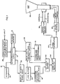
- Figure 1 is an electrical schematic of a system 10 embodying this invention for providing character fonts to a display device in the form of a color cathode ray tube.
- the system 10 which provides a color graphic cathode ray tube display using writeable character fonts, includes a. microprocessor 12 having a program memory 14 associated therewith, a character generator in the form of a read only memory (ROM) 16, a programmable character generator in the form of a random access memory (RAM) 18, a display memory 20 and a video generator 22.
- ROM read only memory
- RAM random access memory
- the microprocessor 12 (central processing unit) controls the flow of information throughout the system 10 under the direction of the program memory 14.
- the program memory 14 typically is contained in the microprocessor 12 but may be separate therefrom if the microprocessor 12 does not contain sufficient memory capacity.
- a data entry keyboard 24 and a communications input 26, for the entry of data from another computer, etc. are provided and can access the microprocessor 12 in order to enter and/or modify data within the program memory 14 or the programmable character generator (RAM) 18.
- the microprocessor 12 can access the display memory 20 or the read-write isolation and control circuitry, shown generally as numeral 28, through which it has access to the programmable character generator (RAM) 18.
- the program memory 14 is programmed to select the proper character generator and does so through the display memory 20 which has character codes (ASCII), used as address information, stored therein.
- the display memory 20, through a line buffer 30, accesses either the programmable character generator (RAM) 18, via the isolation and control circuitry 28, or the character generator (ROM) 16.
- RAM programmable character generator
- ROM character generator
- the contents of the proper memory location associated with the character code (ASCII) is transferred to a tri-state buffer 32.
- this transfer is directly from this generator 16 to the buffer 32, whereas if the programmable character generator (RAM) is utilized, the transfer of the contents of the proper memory location in the character generator 18 to the buffer 32 occurs via the isolation and control circuitry 28.
- the output of the buffer 32 is connected to the input to a video shift register 34 whose output is connected to the input to the video generator 22.
- the output of the video generator 22 is connected to a sweep deflection driver 36 which controls the horizontal and vertical sweeps on a cathode ray tube 38 and is also connected to color drivers 40 which control the red, blue and green colors on the cathode ray tube 38.
- writeable character fonts formed by dots within a dot matrix, are produced and the resulting characters are displayed in fixed rows and columns, typically 80 columns by 48 rows, on the cathode ray tube 38.
- Figure 2 illustrates an eight bit address and an eight bit isolation system. Such isolation is required to permit the microprocessor 12 to program the character generator 18 and to then permit the character generator 18 to subsequently provide data to the video generator 22.
- This isolation and control circuitry 28 comprises
- the address bus from the microprocessor 12 is connected to one input to each of the AND gates A to A 8 , while the other input to each of these gates A 1 to A 8 is connected to the output of the amplifier B 2 whose input is connected to the program command bus of the microprocessor 12.
- the address bus from the display memory 20 is connected to one input to each of the AND gates A 9 to A 16 , while the other input to each of these gates A 9 to A 16 is connected to the output of the inverter B 1 whose input is also connected to the program command bus of the microprocessor 12.
- the outputs of the gates A 1 to A 8 and gates A 9 to A 16 are respectively connected together and the resulting connections form an input to the programmable character generator (RAM) 18.
- the data bus from the microprocessor 12 is connected to one input to each of the AND gates D 1 to D 8 , while the other input to each of these gates D 1 to D 8 is connected to the output of the amplifier B 3 whose input is connected to the program command bus of the microprocessor 12.
- the outputs of these gates D to D 8 are respectively connected to the inputs to AND gates D 9 to D 16 and form another input to the programmable character generator (RAM) 18.
- the other input to each of these AND gates D 9 to D 16 is connected to the output of the inverter B 4 whose input is connected to the program.command bus of the microprocessor 12.
- the outputs of the gates D 9 to D 16 are connected to the input to the tri-state buffer 28.
- the microprocessor 12 programs the display memory 20 with character codes (ASCII) corresponding to the addresses of the characters required.
- ASCII character codes
- the character generator (ROM) 16 receives a particular address from the display memory 20, it outputs the digital equivalent of the character required through the tri-state buffer 32 to the video shift register 34 which, in turn, transmits these data to the video generator 22.
- the microprocessor 12 can program the character generator (RAM) 18 which can then act as a special character generator.
- the display memory 20, through the line buffer 30, can select either the programmable character generator (RAM) 18 or the character generator (ROM) 16 and transfer the data contained therein to the tri-state buffer 32 and then to the video shift register 34 for transmission of same to the video generator 22.
- a program command signal in the form of a digital (1) is received on the program command bus from the microprocessor 12.
- This digital (1) is inverted by the inverter B to a digital (0) which is applied to an input to each of the AND gates A 9 to A 16 disabling all of these gates and preventing the address bus from the display memory 20 from accessing the programmable character generator (RAM) 18.
- this digital (1) signal passes through amplifier B 2 and is applied to an input to each of the AND gates A 1 to A 8 enabling same permitting the address bus from the microprocessor 12 to access the programmable character generator (RAM)18.
- this digital (1) is applied to an input to each of the AND gates D 1 to D 8 enabling same permitting the data bus from the microprocessor 12 to gain access to the programmable character generator (RAM) 18.
- This same digital (1) signal is inverted by inverter B 4 to a digital (0) which is applied to an input to each of,the AND gates Dg through D 16 disabling same preventing the data bus from the microprocessor 12 from transmitting data directly to the tri-state buffer 32. In this manner, the microprocessor 12 can address the programmable character generator (RAM) 18.
- the display memory 20 transmits a particular address along its address bus to the character generator 16.
- the character generator 16 transmits the digital equivalent of the characters required to the tri-state buffer 32 which, in turn, transmits these data to the video shift register 34.
- a program command signal in the form of a digital (0) is transmitted by the microprocessor 12 on the program command bus.
- This digital (0) signal is transformed into a digital (1) by the inverter B 1 causing the AND gates Ag to A 16 to be enabled allowing the address bus for the display memory 20 to access the programmable character generator (RAM)18.
- the foregoing digital (0) also disables AND gates A 1 to A 8 and D 1 to D 8 preventing the address bus and the data bus from the microprocessor 12 from accessing the programmable character generator (RAM) 18. While this is occurring, this digital (0) signal is inverted by inverter B 4 to a digital (1) resulting in the enabling of AND gates D 9 to D 16 .
- the display memory 20 can then access the programmable character generator (RAM) 18 directly which, in turn, transmits the digital equivalent of the character required to the tri-state buffer 32 via the AND gates D 9 to D 16 .
- the tri-state buffer 32 then transmits these data to the video shift register 34. In this manner, the character generator memory capacity has been effectively expanded by the capacity of the programmable character generator (RAM) 18.
Landscapes
- Engineering & Computer Science (AREA)
- Physics & Mathematics (AREA)
- Computer Hardware Design (AREA)
- General Physics & Mathematics (AREA)
- Theoretical Computer Science (AREA)
- Controls And Circuits For Display Device (AREA)
Applications Claiming Priority (2)
| Application Number | Priority Date | Filing Date | Title |
|---|---|---|---|
| US40584182A | 1982-08-06 | 1982-08-06 | |
| US405841 | 1982-08-06 |
Publications (3)
| Publication Number | Publication Date |
|---|---|
| EP0102750A2 true EP0102750A2 (de) | 1984-03-14 |
| EP0102750A3 EP0102750A3 (en) | 1986-08-06 |
| EP0102750B1 EP0102750B1 (de) | 1989-12-06 |
Family
ID=23605471
Family Applications (1)
| Application Number | Title | Priority Date | Filing Date |
|---|---|---|---|
| EP19830304381 Expired EP0102750B1 (de) | 1982-08-06 | 1983-07-28 | Zeichensatzanzeigeeinrichtung |
Country Status (6)
| Country | Link |
|---|---|
| EP (1) | EP0102750B1 (de) |
| JP (2) | JPS5958475A (de) |
| AU (1) | AU555262B2 (de) |
| CA (1) | CA1224289A (de) |
| DE (1) | DE3380944D1 (de) |
| IN (1) | IN159329B (de) |
Cited By (3)
| Publication number | Priority date | Publication date | Assignee | Title |
|---|---|---|---|---|
| EP0199863A1 (de) * | 1985-04-26 | 1986-11-05 | International Business Machines Corporation | Anzeigeeinheit mit Zeichenüberlagerung |
| EP0134423A3 (de) * | 1983-06-13 | 1988-10-05 | Bull HN Information Systems Inc. | Einlesbares Zeichengeneratorgerät und Verfahren zum Einlesen desselben |
| GB2262192A (en) * | 1991-11-28 | 1993-06-09 | Zortech Int | Insulated duct for electric cables |
Families Citing this family (1)
| Publication number | Priority date | Publication date | Assignee | Title |
|---|---|---|---|---|
| JP4781488B1 (ja) * | 2011-02-25 | 2011-09-28 | 有限会社ピーシーエス | コンピューター出力用の「サイド針金付き連続荷札」(ライン荷札) |
Family Cites Families (8)
| Publication number | Priority date | Publication date | Assignee | Title |
|---|---|---|---|---|
| US3729730A (en) * | 1971-04-14 | 1973-04-24 | Cogar Corp | Display system |
| GB1513179A (en) * | 1975-11-17 | 1978-06-07 | British Broadcasting Corp | Data display apparatus |
| JPS52153632A (en) * | 1976-06-16 | 1977-12-20 | Toshiba Corp | Memory correction system |
| FR2419623A1 (fr) * | 1978-03-10 | 1979-10-05 | Telediffusion Fse | Systeme de transmission numerique et d'affichage de textes et de graphismes sur un ecran de television |
| JPS5567843A (en) * | 1978-11-17 | 1980-05-22 | Casio Comput Co Ltd | Pattern data generator |
| JPS5576429A (en) * | 1978-12-01 | 1980-06-09 | Toshiba Corp | Display unit |
| JPS57136682A (en) * | 1981-02-19 | 1982-08-23 | Oki Electric Ind Co Ltd | Foreign language processing system for online terminal |
| JPS5838992A (ja) * | 1981-09-02 | 1983-03-07 | キヤノン株式会社 | 表示パタ−ン発生装置 |
-
1983
- 1983-06-24 AU AU16241/83A patent/AU555262B2/en not_active Ceased
- 1983-07-28 EP EP19830304381 patent/EP0102750B1/de not_active Expired
- 1983-07-28 DE DE8383304381T patent/DE3380944D1/de not_active Expired - Fee Related
- 1983-08-03 IN IN967/CAL/83A patent/IN159329B/en unknown
- 1983-08-05 JP JP58142612A patent/JPS5958475A/ja active Pending
- 1983-08-05 CA CA000433966A patent/CA1224289A/en not_active Expired
-
1991
- 1991-03-19 JP JP2374591U patent/JPH0489996U/ja active Pending
Cited By (4)
| Publication number | Priority date | Publication date | Assignee | Title |
|---|---|---|---|---|
| EP0134423A3 (de) * | 1983-06-13 | 1988-10-05 | Bull HN Information Systems Inc. | Einlesbares Zeichengeneratorgerät und Verfahren zum Einlesen desselben |
| EP0199863A1 (de) * | 1985-04-26 | 1986-11-05 | International Business Machines Corporation | Anzeigeeinheit mit Zeichenüberlagerung |
| US4740783A (en) * | 1985-04-26 | 1988-04-26 | International Business Machines Corporation | Visual display unit with character overstrike |
| GB2262192A (en) * | 1991-11-28 | 1993-06-09 | Zortech Int | Insulated duct for electric cables |
Also Published As
| Publication number | Publication date |
|---|---|
| DE3380944D1 (de) | 1990-01-11 |
| JPH0489996U (de) | 1992-08-05 |
| CA1224289A (en) | 1987-07-14 |
| EP0102750A3 (en) | 1986-08-06 |
| AU1624183A (en) | 1984-02-09 |
| JPS5958475A (ja) | 1984-04-04 |
| EP0102750B1 (de) | 1989-12-06 |
| IN159329B (de) | 1987-05-02 |
| AU555262B2 (en) | 1986-09-18 |
Similar Documents
| Publication | Publication Date | Title |
|---|---|---|
| US4290063A (en) | Video display terminal having means for altering data words | |
| EP0009593B1 (de) | Anzeigevorrichtung mit verteiltem Bildschirm | |
| US4075620A (en) | Video display system | |
| US4682161A (en) | Variable size character display without loss of obscured character positions | |
| US4486856A (en) | Cache memory and control circuit | |
| EP0215984B1 (de) | Graphik-Anzeigegerät mit kombiniertem Bitpuffer und Zeichengraphikspeicherung | |
| US4737779A (en) | Data processing apparatus with dot character generator | |
| EP0032942B1 (de) | Video-anzeige-station | |
| EP0349145B1 (de) | Attributgenerator für ein flaches Bildschirmanzeigegerät | |
| EP0102750A2 (de) | Zeichensatzanzeigeeinrichtung | |
| US4763118A (en) | Graphic display system for personal computer | |
| US4625203A (en) | Arrangement for providing data signals for a data display system | |
| US4712188A (en) | Pattern output apparatus | |
| EP0337752B1 (de) | Graphisches Anzeigesystem zum Ausschneiden eines Teilbildes | |
| EP0420291B1 (de) | Anzeigesteuergerät | |
| JP2846357B2 (ja) | フォントメモリ装置 | |
| EP0292550B1 (de) | Gerät zur anzeigesteuerung von zeichen, denen visuelle attribute hinzugefügt sind | |
| KR900005589B1 (ko) | Lcd 디스플레이 인터페이스회로 | |
| JPS5853338B2 (ja) | ドツト・トパタ−ン出力方式 | |
| EP0272006A2 (de) | Anzeigen-Steuereinrichtung für Datenverarbeitungsgeräte | |
| JPS6161117B2 (de) | ||
| JPS637392B2 (de) | ||
| JPH03192294A (ja) | 表示制御装置 | |
| JPS58158684A (ja) | デイスプレイ制御装置 | |
| JPS6014285A (ja) | デ−タ処理装置 |
Legal Events
| Date | Code | Title | Description |
|---|---|---|---|
| PUAI | Public reference made under article 153(3) epc to a published international application that has entered the european phase |
Free format text: ORIGINAL CODE: 0009012 |
|
| AK | Designated contracting states |
Designated state(s): DE FR GB IT |
|
| PUAL | Search report despatched |
Free format text: ORIGINAL CODE: 0009013 |
|
| AK | Designated contracting states |
Kind code of ref document: A3 Designated state(s): DE FR GB IT |
|
| 17P | Request for examination filed |
Effective date: 19870104 |
|
| 17Q | First examination report despatched |
Effective date: 19881017 |
|
| ITF | It: translation for a ep patent filed | ||
| GRAA | (expected) grant |
Free format text: ORIGINAL CODE: 0009210 |
|
| AK | Designated contracting states |
Kind code of ref document: B1 Designated state(s): DE FR GB IT |
|
| REF | Corresponds to: |
Ref document number: 3380944 Country of ref document: DE Date of ref document: 19900111 |
|
| ET | Fr: translation filed | ||
| PGFP | Annual fee paid to national office [announced via postgrant information from national office to epo] |
Ref country code: GB Payment date: 19900625 Year of fee payment: 8 |
|
| PGFP | Annual fee paid to national office [announced via postgrant information from national office to epo] |
Ref country code: FR Payment date: 19900718 Year of fee payment: 8 |
|
| PGFP | Annual fee paid to national office [announced via postgrant information from national office to epo] |
Ref country code: DE Payment date: 19900726 Year of fee payment: 8 |
|
| ITTA | It: last paid annual fee | ||
| PLBE | No opposition filed within time limit |
Free format text: ORIGINAL CODE: 0009261 |
|
| STAA | Information on the status of an ep patent application or granted ep patent |
Free format text: STATUS: NO OPPOSITION FILED WITHIN TIME LIMIT |
|
| 26N | No opposition filed | ||
| PG25 | Lapsed in a contracting state [announced via postgrant information from national office to epo] |
Ref country code: GB Effective date: 19910728 |
|
| GBPC | Gb: european patent ceased through non-payment of renewal fee | ||
| PG25 | Lapsed in a contracting state [announced via postgrant information from national office to epo] |
Ref country code: FR Effective date: 19920331 |
|
| PG25 | Lapsed in a contracting state [announced via postgrant information from national office to epo] |
Ref country code: DE Effective date: 19920401 |
|
| REG | Reference to a national code |
Ref country code: FR Ref legal event code: ST |