EP0102946B1 - Gain regulation circuit - Google Patents
Gain regulation circuit Download PDFInfo
- Publication number
- EP0102946B1 EP0102946B1 EP82900646A EP82900646A EP0102946B1 EP 0102946 B1 EP0102946 B1 EP 0102946B1 EP 82900646 A EP82900646 A EP 82900646A EP 82900646 A EP82900646 A EP 82900646A EP 0102946 B1 EP0102946 B1 EP 0102946B1
- Authority
- EP
- European Patent Office
- Prior art keywords
- gain
- pairs
- circuit
- pair
- long tailed
- Prior art date
- Legal status (The legal status is an assumption and is not a legal conclusion. Google has not performed a legal analysis and makes no representation as to the accuracy of the status listed.)
- Expired
Links
Images

Classifications
-
- H—ELECTRICITY
- H03—ELECTRONIC CIRCUITRY
- H03F—AMPLIFIERS
- H03F3/00—Amplifiers with only discharge tubes or only semiconductor devices as amplifying elements
- H03F3/45—Differential amplifiers
- H03F3/45071—Differential amplifiers with semiconductor devices only
- H03F3/45076—Differential amplifiers with semiconductor devices only characterised by the way of implementation of the active amplifying circuit in the differential amplifier
- H03F3/4508—Differential amplifiers with semiconductor devices only characterised by the way of implementation of the active amplifying circuit in the differential amplifier using bipolar transistors as the active amplifying circuit
- H03F3/45085—Long tailed pairs
-
- H—ELECTRICITY
- H03—ELECTRONIC CIRCUITRY
- H03G—CONTROL OF AMPLIFICATION
- H03G11/00—Limiting amplitude; Limiting rate of change of amplitude
- H03G11/002—Limiting amplitude; Limiting rate of change of amplitude without controlling loop
-
- H—ELECTRICITY
- H03—ELECTRONIC CIRCUITRY
- H03G—CONTROL OF AMPLIFICATION
- H03G3/00—Gain control in amplifiers or frequency changers
- H03G3/20—Automatic control
- H03G3/30—Automatic control in amplifiers having semiconductor devices
- H03G3/3005—Automatic control in amplifiers having semiconductor devices in amplifiers suitable for low-frequencies, e.g. audio amplifiers
-
- H—ELECTRICITY
- H04—ELECTRIC COMMUNICATION TECHNIQUE
- H04M—TELEPHONIC COMMUNICATION
- H04M1/00—Substation equipment, e.g. for use by subscribers
- H04M1/738—Interface circuits for coupling substations to external telephone lines
- H04M1/76—Compensating for differences in line impedance
-
- E—FIXED CONSTRUCTIONS
- E06—DOORS, WINDOWS, SHUTTERS, OR ROLLER BLINDS IN GENERAL; LADDERS
- E06B—FIXED OR MOVABLE CLOSURES FOR OPENINGS IN BUILDINGS, VEHICLES, FENCES OR LIKE ENCLOSURES IN GENERAL, e.g. DOORS, WINDOWS, BLINDS, GATES
- E06B7/00—Special arrangements or measures in connection with doors or windows
- E06B7/02—Special arrangements or measures in connection with doors or windows for providing ventilation, e.g. through double windows; Arrangement of ventilation roses
- E06B2007/026—Special arrangements or measures in connection with doors or windows for providing ventilation, e.g. through double windows; Arrangement of ventilation roses with air flow between panes
-
- H—ELECTRICITY
- H03—ELECTRONIC CIRCUITRY
- H03F—AMPLIFIERS
- H03F2203/00—Indexing scheme relating to amplifiers with only discharge tubes or only semiconductor devices as amplifying elements covered by H03F3/00
- H03F2203/45—Indexing scheme relating to differential amplifiers
- H03F2203/45362—Indexing scheme relating to differential amplifiers the AAC comprising multiple transistors parallel coupled at their gates and drains only, e.g. in a cascode dif amp, only those forming the composite common source transistor
Definitions
- This invention relates to electronic amplifier circuits.having a regulatable gain, and in particular to a gain regulation circuit for use in a telephone instrument and whereby the gain of the instrument speech paths may be adjusted e.g. for matching the receiver gain to the line loop impedance.
- An electronic telephone instrument includes an amplifying speech path whereby speech signals are relayed from the instrument microphone to the line and from the line to the instrument receiver. It will be appreciated that for optimum performance of the instrument the receiver and transmitter speech paths must each include some means of gain regulation to prevent overloading and to provide matching of the receiver gain to the line impedance.
- the line or loop impedance is in general proportional to the length of the subscriber loop between the instrument and the exchange and can thus have any value within a clearly defined range. Because it is necessary to cater for a wide variation of loop length, it is essential that the receiver circuit of the subscriber's instrument incorporates provision for line length compensation. To compensate loop length variatons many telephone administrations require the provision of receiver circuits that can be set to a gain figure anywhere between upper and lower preset limits..
- a particularly useful variable gain element is the transistor long tailed pair the gain of which can be determined by controlling the common emitter current of the pair.
- the use of a single long tailed pair is however somewhat restricted by its significantly non linear signal/gain characteristic which gives rise to distortion for all but very low signal levels. In some applications this distortion may be outside the limits specified by the telephone administration.
- amplifier circuits incorporating a first and second long tailed transistor pair connected in parallel have been described e.g. in FR-A-2,482,385 and CA-A-923573.
- the first pair defines the gain of the arrangement whilst the second pair, applied with -a reference voltage, provides a gain limitation function to prevent an excessive signal output for the circuit.
- Neither of these circuits however provides the desired effect of a stage gain that is smoothly adjustable between two defined limits.
- the object of the present invention is to provide a gain regulation circuit whereby a smooth and continuous gain variation between predefined limits in response to a control signal may be effected.
- a signal amplifier e.g. for a telephone subset provided with automatic gain control
- the gain determining element comprises a plurality of long tailed transistor pairs coupled in parallel, characterised in that said long tailed pairs consist of a first transistor (TR51, TR52) pair and 2n further transistor pairs (E1B, E2B, E1C, E2C) where n is an integer including unity, that the transistors of the first pair have substantially identical characteristics, that corresponding transistors of the 2n further pairs have emitter areas in the ratio 1:a; a: 1, where a lies between zero and unity, whereby the gain maxima of the characteristics of the further long tailed pairs are symmetrically disposed about the signal zero so as to provide together a substantially constant gain region of significantly lower gain than the gain maximum of the first long tailed pair, and that the outputs of the long tailed pairs are combined so as to provide a stage gain continuously adjustable between limits defined by the gain of the first pair and the gain of the further pairs.
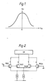
- Fig. 1 the signal/gain characteristic of a conventional transistor long tailed pair is shown.
- the gain g of a balanced, i.e. a symmetrical long tailed pair is defined by where q is the electronic charge, I is the tail current of the pair, k is Boltzman's constant, t is the absolute temperature and Vin is the instantaneous input signal level.
- q is the electronic charge
- I is the tail current of the pair
- k is Boltzman's constant
- t is the absolute temperature
- Vin the instantaneous input signal level.
- the characteristic has the appearance of a somewhat distorted inverted U and it will thus be apparent that low distortion amplification is achieved only for a small input signal voltage swing.
- the circuit has substantially unit gain.
- the resultant gain characteristic of the two pairs is shown by the dashed line in Fig. 3.
- the characteristic With a suitable choice of the area ratio a, typically from 1/5 to 1/12, the characteristic has a substantially constant region of gain a, less than unity, extending V either side of the signal zero. This considerably enhances the low distortion signal handling capability of the circuit as compared to a conventional single long tailed pair amplifier. In this circuit gain has been traded for signal handling capability.
- Fig. 4 illustrates the gain characteristics of a circuit comprising three long tailed pairs wherein the respective emitter area ratios of the pairs of transistors are 1:a; 1:1 and a:1.
- the circuit can be set in a high (unit) gain condition wherein the balanced long tailed pair acts as the major amplifying element, or to a low (a) gain condition wherein the unbalanced long tailed pairs act as the major amplifying element. Weighted combinations of these two states can be employed to provide any gain value between these limits.
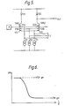
- Fig. 5 of the accompanying drawings is a circuit diagram of a gain regulation circuit stage e.g. from the receiver speech path of an electronic telephone subset.
- the circuit output is coupled to the line via a further linear amplifier stage (not shown).
- the gain In order to comply with the design specifications of most telephone administrations it is necessary to provide some means of gain control to compensate for the range of different line loop lengths between the exchange and the subscribers. Typically the gain must be variable between two limits which represent the 'best case' and 'worst case' loop lengths. The gain must be continuously and smoothly variable between these limits. A circuit which satisfies these constraints is shown in Fig. 5.
- the gain regulation circuit provides an accurately defined gain of any value between first and second predetermined levels.
- the circuit comprises first and second multi-emitter transistors TR51 and TR52 arranged in a multiple long-tailed pair configuration. Corresponding pairs of emitters E1A, E2A; E1B, E2B; E1C; E2C are coupled each to a corresponding current source 11,12,13 arranged in the "tail circuit' of the pair.
- the transistor collector loads may be provided by forward biased diodes D1 and D2, which provide temperature compensation of the circuit.
- the impedance R of a diode is given by the expression: where k is Boltzmann's constant, t is the absolute temperature, q is the electronic charge and I is the current in absolute units. It will be noted that this impedance expression is the increase of the temperature dependent term of the gain expression:
- the transistors TR51 and TR52 are fabricated such that the first emitters E1A and E2A are of substantially equal area, i.e. they are capable of carrying substantially equal currents.
- the second pair of emitters E1B, E2B have areas in the ratio 1:a and the third pair E1C, E2C have areas in the ratio a:1 where a is an arbitrary fraction between zero and unity.
- Such a structure has the propertythat, in the absence of an inputsignai,the currents flowing through the respective pairs of emitters are in the ratio 1:1, 1:a and a:1.
- the circuit has two gain limits (Fig. 4) of unity and a and is adjustable to any value between these limits.
- the ratio 1:a is equal to the ratio of the receiver gain value limits specified by the receiver gain value limits specified by the telephone administration. This ensures that the overall gain of the receiver channel can be set to any value within these limits.
- the arrangement may provide a gain regulation feedback loop for an amplifier whereby speech signals are output to the line.
- the bases of the transistors TR51 and TR52 are connected respectively to the speech signal and to a fixed or reference potential source at P.
- the emitter circuits are fed, via a current amplifier (not shown), with currents corresponding to the line voltage. It will be appreciated that this line voltage is inversely proportional to the subscriber loop impedance.
- the line impedance is determined from the line voltage and corresponding currents are then fed to the rail circuits of the long tailed pairs to provide a corresponding gain value.
- the gain condition of the circuit is determined by the weighted contributions of the balanced and unbalanced pairs in the composite output characteristic.
- the gain condition of the circuit is determined by the weighted contributions of the balanced and unbalanced pairs in the composite output characteristic.
- I" 1 2 , 1 3 fed into the tail circuit of the transistor pairs the contribution of each pair can be correspondingly reduced or increased.
- This provides a smooth transfer, as shown in Fig. 6, from a unit gain condition wherein the balanced pair provides the major contribution to the output signal to a low (a) gain condition where the unbalanced pairs handle the major portion of the signal and the contribution of the balanced pair is reduced substantially to zero.
- the circuit may be set to any gain value between these two limit conditions.
- the arrangement is equivalent to a plurality of long-tailed pairs arranged in parallel, the no-signal balance currents of each pair being defined by the emitter area ratio of the pair.
Landscapes
- Engineering & Computer Science (AREA)
- Power Engineering (AREA)
- Signal Processing (AREA)
- Multimedia (AREA)
- Amplifiers (AREA)
- Interface Circuits In Exchanges (AREA)
Applications Claiming Priority (1)
| Application Number | Priority Date | Filing Date | Title |
|---|---|---|---|
| PCT/GB1982/000070 WO1983003177A1 (en) | 1982-03-04 | 1982-03-04 | Gain regulation circuit |
Publications (2)
| Publication Number | Publication Date |
|---|---|
| EP0102946A1 EP0102946A1 (en) | 1984-03-21 |
| EP0102946B1 true EP0102946B1 (en) | 1987-10-14 |
Family
ID=10527414
Family Applications (1)
| Application Number | Title | Priority Date | Filing Date |
|---|---|---|---|
| EP82900646A Expired EP0102946B1 (en) | 1982-03-04 | 1982-03-04 | Gain regulation circuit |
Country Status (7)
| Country | Link |
|---|---|
| US (1) | US4502018A (da) |
| EP (1) | EP0102946B1 (da) |
| JP (1) | JPS59500344A (da) |
| DE (1) | DE3277492D1 (da) |
| DK (1) | DK503183D0 (da) |
| NZ (1) | NZ203388A (da) |
| WO (1) | WO1983003177A1 (da) |
Cited By (1)
| Publication number | Priority date | Publication date | Assignee | Title |
|---|---|---|---|---|
| WO1996013896A3 (en) * | 1994-10-28 | 1996-11-21 | Philips Electronics Nv | A gain controllable amplifier, a receiver comprising a gain-controllable amplifier, and a method of controlling signal amplitudes |
Families Citing this family (4)
| Publication number | Priority date | Publication date | Assignee | Title |
|---|---|---|---|---|
| US4833422A (en) * | 1987-09-24 | 1989-05-23 | Burr-Brown Corporation | Programmable gain instrumentation amplifier |
| SE505403C2 (sv) * | 1995-11-30 | 1997-08-18 | Ericsson Telefon Ab L M | Förfarande för reducering av transienter i ett redundant klocksignalgenererande system |
| DE102005054216B4 (de) * | 2004-11-25 | 2017-10-12 | Infineon Technologies Ag | Ausgangsstufe, Verstärkerregelschleife und Verwendung der Ausgangsstufe |
| JP5744463B2 (ja) * | 2010-10-14 | 2015-07-08 | キヤノン株式会社 | 光電変換装置 |
Family Cites Families (9)
| Publication number | Priority date | Publication date | Assignee | Title |
|---|---|---|---|---|
| DE2037695A1 (de) * | 1970-07-29 | 1972-02-10 | Siemens Ag | Integrierter Differenzverstärker mit gesteuerter Gegenkopplung |
| CA923573A (en) * | 1971-03-11 | 1973-03-27 | Northern Electric Company | Automatic gain control circuit |
| GB1406603A (en) * | 1971-07-23 | 1975-09-17 | Steiner Ltd H | Road planing machines |
| NL7115947A (da) * | 1971-11-19 | 1973-05-22 | ||
| GB1406663A (en) * | 1972-08-22 | 1975-09-17 | Standard Telephones Cables Ltd | Telphone subset circuits |
| JPS5625815B2 (da) * | 1974-02-14 | 1981-06-15 | ||
| JPS5494213A (en) * | 1978-01-10 | 1979-07-25 | Nec Corp | Amplifier for transmitter |
| JPS5928307B2 (ja) * | 1979-05-16 | 1984-07-12 | 日本電信電話株式会社 | 電話機用ダイヤル信号自動レベル調整回路 |
| FR2482385B1 (fr) * | 1980-05-09 | 1986-04-04 | Ericsson Telefon Ab L M | Circuit de reglage de gain |
-
1982
- 1982-03-04 JP JP57500817A patent/JPS59500344A/ja active Pending
- 1982-03-04 EP EP82900646A patent/EP0102946B1/en not_active Expired
- 1982-03-04 US US06/491,688 patent/US4502018A/en not_active Expired - Fee Related
- 1982-03-04 DE DE8282900646T patent/DE3277492D1/de not_active Expired
- 1982-03-04 WO PCT/GB1982/000070 patent/WO1983003177A1/en not_active Ceased
-
1983
- 1983-02-24 NZ NZ203388A patent/NZ203388A/en unknown
- 1983-11-03 DK DK503183A patent/DK503183D0/da not_active Application Discontinuation
Cited By (2)
| Publication number | Priority date | Publication date | Assignee | Title |
|---|---|---|---|---|
| WO1996013896A3 (en) * | 1994-10-28 | 1996-11-21 | Philips Electronics Nv | A gain controllable amplifier, a receiver comprising a gain-controllable amplifier, and a method of controlling signal amplitudes |
| US5742203A (en) * | 1994-10-28 | 1998-04-21 | U.S. Philips Corporation | Gain-controllable amplifier, receiver |
Also Published As
| Publication number | Publication date |
|---|---|
| DE3277492D1 (en) | 1987-11-19 |
| US4502018A (en) | 1985-02-26 |
| DK503183A (da) | 1983-11-03 |
| NZ203388A (en) | 1986-01-24 |
| JPS59500344A (ja) | 1984-03-01 |
| WO1983003177A1 (en) | 1983-09-15 |
| EP0102946A1 (en) | 1984-03-21 |
| DK503183D0 (da) | 1983-11-03 |
Similar Documents
| Publication | Publication Date | Title |
|---|---|---|
| US3991380A (en) | Complementary field effect transistor differential amplifier | |
| US5187448A (en) | Differential amplifier with common-mode stability enhancement | |
| US6011437A (en) | High precision, high bandwidth variable gain amplifier and method | |
| US4427903A (en) | Voltage current converter circuit | |
| US5999052A (en) | High speed, fine-resolution gain programmable amplifier | |
| US5742203A (en) | Gain-controllable amplifier, receiver | |
| EP0037406B1 (en) | Cmos operational amplifier with reduced power dissipation | |
| CA2324109A1 (en) | Wide-dynamic-range variable-gain amplifier | |
| US5389893A (en) | Circuit for a controllable amplifier | |
| US3786362A (en) | Balanced output operational amplifier | |
| US4870372A (en) | AGC delay on an integrated circuit | |
| EP1119100B1 (en) | Amplifiers | |
| US4502018A (en) | Gain regulation circuit for an amplifier circuit | |
| US5382919A (en) | Wideband constant impedance amplifiers | |
| US4918401A (en) | Step adjustable distributed amplifier network structure | |
| JPH10126179A (ja) | 利得制御回路及び方法 | |
| US5028882A (en) | Multiple output operational amplifier | |
| US4716378A (en) | Amplifier circuit | |
| CA1200941A (en) | Gain regulation circuit | |
| US5351011A (en) | Low noise, low distortion MOS amplifier circuit | |
| US3854101A (en) | Differential amplifiers | |
| US5170134A (en) | Fast buffer | |
| US5166983A (en) | Mute circuit for audio amplifiers | |
| US5023564A (en) | Amplfier circuit | |
| US20260100685A1 (en) | Current mirror operational transconductance amplifier |
Legal Events
| Date | Code | Title | Description |
|---|---|---|---|
| PUAI | Public reference made under article 153(3) epc to a published international application that has entered the european phase |
Free format text: ORIGINAL CODE: 0009012 |
|
| 17P | Request for examination filed |
Effective date: 19831021 |
|
| AK | Designated contracting states |
Kind code of ref document: A1 Designated state(s): BE DE FR GB NL SE |
|
| RAP1 | Party data changed (applicant data changed or rights of an application transferred) |
Owner name: INTERNATIONAL STANDARD ELECTRIC CORPORATION Owner name: STC PLC |
|
| RAP1 | Party data changed (applicant data changed or rights of an application transferred) |
Owner name: INTERNATIONAL STANDARD ELECTRIC CORPORATION Owner name: STC PLC |
|
| GRAA | (expected) grant |
Free format text: ORIGINAL CODE: 0009210 |
|
| AK | Designated contracting states |
Kind code of ref document: B1 Designated state(s): BE DE FR GB NL SE |
|
| PG25 | Lapsed in a contracting state [announced via postgrant information from national office to epo] |
Ref country code: NL Effective date: 19871014 Ref country code: BE Effective date: 19871014 |
|
| REF | Corresponds to: |
Ref document number: 3277492 Country of ref document: DE Date of ref document: 19871119 |
|
| ET | Fr: translation filed | ||
| PG25 | Lapsed in a contracting state [announced via postgrant information from national office to epo] |
Ref country code: SE Effective date: 19880305 |
|
| NLV1 | Nl: lapsed or annulled due to failure to fulfill the requirements of art. 29p and 29m of the patents act | ||
| PLBE | No opposition filed within time limit |
Free format text: ORIGINAL CODE: 0009261 |
|
| STAA | Information on the status of an ep patent application or granted ep patent |
Free format text: STATUS: NO OPPOSITION FILED WITHIN TIME LIMIT |
|
| 26N | No opposition filed | ||
| PG25 | Lapsed in a contracting state [announced via postgrant information from national office to epo] |
Ref country code: FR Free format text: LAPSE BECAUSE OF NON-PAYMENT OF DUE FEES Effective date: 19891130 |
|
| REG | Reference to a national code |
Ref country code: FR Ref legal event code: ST |
|
| REG | Reference to a national code |
Ref country code: GB Ref legal event code: 732E |
|
| EUG | Se: european patent has lapsed |
Ref document number: 82900646.9 Effective date: 19881206 |
|
| PGFP | Annual fee paid to national office [announced via postgrant information from national office to epo] |
Ref country code: GB Payment date: 20010219 Year of fee payment: 20 |
|
| PGFP | Annual fee paid to national office [announced via postgrant information from national office to epo] |
Ref country code: DE Payment date: 20010222 Year of fee payment: 20 |
|
| REG | Reference to a national code |
Ref country code: GB Ref legal event code: IF02 |
|
| PG25 | Lapsed in a contracting state [announced via postgrant information from national office to epo] |
Ref country code: GB Free format text: LAPSE BECAUSE OF EXPIRATION OF PROTECTION Effective date: 20020303 |
|
| REG | Reference to a national code |
Ref country code: GB Ref legal event code: PE20 Effective date: 20020303 |