EP0103629B1 - Procede et appareil pour systemes de detection de vols - Google Patents
Procede et appareil pour systemes de detection de vols Download PDFInfo
- Publication number
- EP0103629B1 EP0103629B1 EP83901292A EP83901292A EP0103629B1 EP 0103629 B1 EP0103629 B1 EP 0103629B1 EP 83901292 A EP83901292 A EP 83901292A EP 83901292 A EP83901292 A EP 83901292A EP 0103629 B1 EP0103629 B1 EP 0103629B1
- Authority
- EP
- European Patent Office
- Prior art keywords
- marker
- signal
- signals
- receiver
- field
- Prior art date
- Legal status (The legal status is an assumption and is not a legal conclusion. Google has not performed a legal analysis and makes no representation as to the accuracy of the status listed.)
- Expired
Links
Images



Classifications
-
- G—PHYSICS
- G08—SIGNALLING
- G08B—SIGNALLING SYSTEMS, e.g. PERSONAL CALLING SYSTEMS; ORDER TELEGRAPHS; ALARM SYSTEMS
- G08B13/00—Burglar, theft or intruder alarms
- G08B13/22—Electrical actuation
- G08B13/24—Electrical actuation by interference with electromagnetic field distribution
- G08B13/2402—Electronic Article Surveillance [EAS], i.e. systems using tags for detecting removal of a tagged item from a secure area, e.g. tags for detecting shoplifting
- G08B13/2405—Electronic Article Surveillance [EAS], i.e. systems using tags for detecting removal of a tagged item from a secure area, e.g. tags for detecting shoplifting characterised by the tag technology used
- G08B13/2408—Electronic Article Surveillance [EAS], i.e. systems using tags for detecting removal of a tagged item from a secure area, e.g. tags for detecting shoplifting characterised by the tag technology used using ferromagnetic tags
Definitions
- This invention relates in a broad sense to detection systems and apparatus, and more particularly to detection systems principally used in "anti-pilfering", i.e., theft-prevention, systems; more particularly still, the invention relates to that type of detection system in which an alternating electromagnetic field is monitored to unobtrusively and invisibly detect the presence within the field of a small strip of permalloy or like highly- magnetizable (ultra-low coercivity) metal foil which is hidden upon or in articles such as consumer merchandise whose theft or otherwise- impermissible taking is to be detected and prevented.
- anti-pilfering i.e., theft-prevention
- Picard noted the field effects created by the presence of highly-magnetic (high permeability) material such as permalloy, which creates the presence of a number of the higher-order odd harmonics of the fundamental frequency of the applied field (e.g., Picard referred to the presence of the ninth and eleventh harmonic). While a period of almost 50 years has elapsed since the appearance of this patent to Picard, various patents continue to issue from time to time asserting advances in Picard's theories and findings in the area of "pilferage detection" systems of the type noted hereinabove; for example, reference is made to a number of patents issued to Edward Fearon (including U.S. Nos.
- the present invention as defined in claims 1 and 26 provides new and highly significant improvements in electromagnetic field-type detection systems of the type noted above, which improvements substantially enhance both the sensitivity and the selectivity of such a system, pursuant to which previously-unappreciated detrimental effects such as field-perturbing metal structural components in the environment of the egress portal (e.g., field-perturbing ceiling grids overhead and/or field-perturbing reinforcing rods or mesh in structural concrete nearby, etc.) are substantially eliminated as error sources.
- field-perturbing metal structural components in the environment of the egress portal e.g., field-perturbing ceiling grids overhead and/or field-perturbing reinforcing rods or mesh in structural concrete nearby, etc.
- the improved system thus makes it possible to accurately, consistently, and reliably detect the presence of tiny markers or tags of magnetic material and reject, or not detect, the presence of other field-disrupting metal elements or components as, for example, keys, pocketknives, wristwatches, metal containers such as beverage cans or the like, baby strollers and shopping carts, and a host of other widely- differing apparatus and objects.
- a detection system and method is provided with greatly enhanced processing of the marker-detection signals, incorporating a summing and differencing procedure for substantially improved signal-to-noise ratios, in accordance with which a comparatively low frequency component band and a comparatively high frequency component band are separately determined, and utilized in a multiple-step comparative manner to dymamically control the detection alarm threshold.
- the method and apparatus operates to additively, or constructively, sum representations of detection signals indicative of marker presence within the field, regardless of and continuously consistent with, field alternation phase changes and differences; additionally, the method and apparatus provided differences or subtracts signals representative of non-marker presence (i.e., noise) in order to accurately portray non-marker effects.
- the marker-characterizing signals are comparatively analyzed by reference to the non-marker signals, thus substantially enhancing selectivity.
- detection logic and processing methods and apparatus are provided for examining representations of electrical signals which are produced initially by receiver means that monitor an alternating electromagnetic interrogation field in which a predetermined marker may be present, so as to accurately and reliably determine the presence, and/or the non- presence, of such a marker in such a field.
- signal-examining is carried out in a manner having the effect of determining, and using, a first and second composite analysis signal, the first being used to set a first value of a comparison operation and the second such signal being used to set a second such comparison value, such two comparison values being effectively compared in such comparison operation.
- this is accomplished by developing an integrated ambient- representative signal and using the latter to vary a preset threshold in comparison stages whose primary comparison inputs are signals representative of marker presence and marker absence, with the results of such comparisons being summed against each other, and the resultant summation level used to trigger an alarm or indicator showing the verified presence of the marker within the interrogation field.
- the inventor provides preferred methods and apparatus for selective preamplification and processing of the signals produced initially by the receiver means, prior to the operation of the preferred detection logic and processing methods and apparatus, both of which are further disclosed in the following description of particular preferred embodiments.
- FIG. 1 The general nature of the overall system is illustrated in Fig. 1, in which a typical two-portal system is depicted.
- such "portals” should be understood as being egress passages, e.g., doorways, on the opposite sides of each of which are maintained electromagnetic interrogation field sources (e.g., induction coils constituting part of an oscillating L-C tank circuit) together with a receiving antenna which monitors the electromagnetic field from that particular side of the portal.
- electromagnetic interrogation field sources e.g., induction coils constituting part of an oscillating L-C tank circuit
- a receiving antenna which monitors the electromagnetic field from that particular side of the portal.
- many of the prior patents referred to hereinabove depict and discuss systems using such interrogation coils and antennae; for example, Richardson U.S. No.
- portal 1 has a pair of oppositely- spaced sides, designated “side 1" and “side 2", and the same is true with respect to portal 2, which may be considered a substantial duplicate of portal 1.
- Each side 1 of each portal preferably receives the same type of drive, i.e., interrogation coil-excitation or drive current and each side 2 coil is also driven like its counterparts, although as explained hereinafter the side 2 excitation preferably changes in phase periodically whereas the side 1 excitation does not.
- the signal path from each side of each portal is individually coupled (via channels or paths. A and A', and Band B') to a preamp 1, from which two outputs are separately processed, one being directed to an amplifier/filter 2 and the other to an inhibit amplifier 3, whose-respective outputs are coupled on paths E and F to a detection logic and processing module 9, which also receives control signals on path G from a timing generator 4.
- the detection logic module 9 functions to provide indicator and/or alarm signals indicative of the presence, within the alternating interrogation field maintained between the respective sides of a given portal, of the desired field-affecting marker member, such indicator or alarm outputs being depicted in Fig.
- Fig. 1 Power supply paths are indicated in Fig. 1 as being directed from an outside "power in” source and along a common bus 11 to a power supply 8.
- the latter provides various power levels and types to the preamp 1, the detection logic module 9, the amp/ filter 2, the inhibit amplifier 3, the timing generator 4, the phase driver control 5, and the phase driver 6.
- the outputs of the phase driver 6 are coupled along the aforementioned paths C and D to portals 1 and 2, to drive the oscillating interrogation coils located there. While state of the art circuits and components which are generally usable as the foregoing functional units are certainly known and available at the present. point in time, and are referred to in the aforementioned prior patents, for example, certain preferred new versions or improvements of such are disclosed hereinafter.
- the interrogation coils at the portals are preferably driven at a nominal oscillation frequency of 10 kHz, and that in order to maximize detection capabilities in a broad sense, it is desirable to drive the two interrogation coils on opposite sides of the same portal in an alternating in-phase and out-of-phase sequence, in "bursts" which continue over a desired number of cycles.
- a particular example of a preferred phase-reversal sequencing comprises alternating bursts of 160 cycles (i.e., 16 msec) of the nominal 10 kHz fundamental alternation, separated by a "dead time” or “inter burst gap” of 4 msec, with the first such 160 cycle burst applied with the same phase condition (e.g., "phase A”) on both sides 1 and 2 of each portal (i.e., "A-A" phasing), and the second such burst applied with "phase A" on side 1 and the opposite (“phase B") applied to side 2 of each portal (i.e., "A-B" phasing).
- phase A phase condition
- phase B opposite
- the antenna at each portal side (constituting the initial "receiving means" herewith) will return in-phase signal components for marker-present conditions within the portal during the first such in-phase drive condition, and out-of-phase marker-present signals during the next such drive condition.
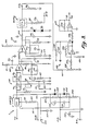
- the detection signals from the antennae at the various portal sides are coupled along signal paths A, A' and B, B' to the preamplifier 1, a detailed illustration of a preferred embodiment of which is set forth in Fig. 2, to which reference is now made.
- the preamp 1 signal paths A and A' from the receivers, or antennae, which monitor side 1 of both portals 1 and 2, are coupled respectively to preamp inputs P-1 and P-2.
- signal paths B and B' from side 2 of both portal 1 and portal 2 are coupled, respectively, to preamp inputs P-3 and P-4.
- each such preamp input feeds into an identically- configured amplifying and filtering network branch, located generally within the circuit portion on the left, designated 1-A, and each of the four such preamplifier/filter network portions feeds into a summation circuit portion on the right, designated 1-B.
- the interrogation field-generating coils are driven, in the alternating- phase sequence noted above, with current pulses on the order of magnitude of approximately 50 amps, preferably once every several cycles of tank circuit oscillation (e.g., every fourth cycle of oscillation), resulting in an oscillation of approximately three hundred volts (peak to peak) in amplitude.
- Each receiving antenna therefore, would nominally detect a very strong 10 kHz signal, and for this reason the antennae are preferably figure-eighted in winding configuration, so as to null out as much as possible of the 10 kHz component.
- the field perturbations caused by the presence within one of the portals of the permalloy strip or other such marker element are miniscule in comparison to the tank drive level, thus presenting very substantial signal-processing difficulties in order to achieve high sensitivity, to avoid missing contraband-carried markers, while at the same time achieving a high degree of selectivity, to avoid erroneous contraband or theft-indicative alarms brought about by any of a variety of metallic objects or articles which also cause perturbations in the interrogation field.
- the drive excitation pulses applied to the field-inducing coils are highly disruptive in and of themselves, and it is thus desirable to blank out all or part of the receiving circuitry during the time such drive pulses are being applied to the interrogation coil.
- the actual permalloy or other such low-coercivity markers create field perturbations by switching their magnetic domain orientation each half-cycle of alternation of the interrogation field, i.e., on each positive-going half-cycle as well as upon each negative-going half-cycle, with magnetic domain switching occurring during the first 90° of current flow in the coils for each such half-cycle.
- the antenna (“receiver means”) signals are examined to determine the presence of a marker within the field only during the current-rise portion of the cycle (i.e., the first 90°), other non-marker perturbations may be screened out.
- a sample of the antenna/receiver means signals is examined during other portions of the cycles of interrogation field alternation, i.e., when marker perturbations are not anticipated (i.e., during the current falling portion of each half-cycle), a representative ambient field condition may be established for comparison with the receiver means signals obtained or examined during those periods when marker signals are to be anticipated if indeed a marker is present within the portal, i.e., within the interrogation field.
- the treatment afforded the receiver means signals prior to actual analysis efforts, whose purpose is to determine whether or not a marker is present, becomes very important to successful processing. That is, while it has heretofore been recognized that the interrogation field fundamental frequency (here, 10 kHz) must be eliminated to the fullest extent possible, the countervailing consideration is to maintain the integrity (fidelity) of the actual signal from the antenna to the greatest extent possible.
- the signals first encounter a Pi-type RC filter 40, which applies an initial attenuation of 6 DB centered upon the 10 kHz drive frequency, but does not introduce any appreciable noise content as other filtering might.
- the receiver signals encounter an amplifying stage 42, which is preferably a low-noise voltage amplifier having a gain on the order of about ten, designated U100.
- the latter is implemented by use of an integrated circuit operational amplifier such as that designated as IC5534 coupled into the circuit in the manner indicated, with resistive feedback. Accordingly, the receiver signals from the antennae essentially encounter strong low-noise amplification prior to operational filtering.
- twin-T notch filter 44 comprised of resistors R107, R108, R109, and capacitors C104, C105, and C106, in which it will be observed that resistors R108 and R109 are variable in nature, to provide for precise setting of the notch characteristics.
- Notch filter 44 is centered upon the 10 kHz interrogation field frequency, and supplies at least 40 DB of rejection for such frequency.
- a buffer stage of amplification 46 which may be implemented by another integrated circuit No. 5534 operational amplifier, configured to provide unity gain. It is to be noted that both amplifiers 42 and 46 should be wide band amplifiers, so as to accommodate all of the frequencies within the range extending from the fundamental of the interrogation field out to at least the fifteenth harmonic thereof. While set forth more fully hereinafter, it is to be noted that the high- order and low-order harmonic content of these antennae signals are utilized as important determinative factors in accordance herewith by observing the ratio or relative amounts of these bands of frequencies.
- the lower-frequency band comprises primarily the third and fifth harmonic range, and to some extent the seventh, since this range is highly representative of interrogation field perturbations brought about by non-marker metal objects of many and different particular natures. That is, the actual permalloy or like marker produces a significantly different ratio of the higher-order harmonic band with respect to the lower-order harmonic band, even though both the authentic marker and other non-marker objects may produce varying amounts of both frequency bands in the responses detected from the field perturbations which they cause.
- some particular and relatively unusual metal objects may to a considerable degree "mimic” (that is, resemble) the response of an authentic permalloy or like marker, although in essentially every instance the actual ratio of the high order harmonic band to the low order band (as defined above) will be at least somewhat different than those brought about by the authentic marker element.
- Each of the preamp circuit paths commencing at the inputs P-1, P-2, etc. thus produces a relatively noise-free and significantly amplified version of the antennae/receiver means signals, with the fundamental 10 kHz signal substantially reduced but with harmonics of this signal present.
- Each such circuit path has a pair of output resistors R111/R112, R211/R212, etc., which are coupled into the summing portion of the preamp 1-B in the following manner. First, it will be noted that the R111-R211 outputs are ganged together and fed to the inverting side of a differential amplifier U102.
- This same circuit path is coupled to the output side of an upper switch portion S, in a four-stage CMOS analog switch S100, through which signals from preamp path P-3 output resistors R311 and R411 may also be coupled, upon appropriate actuation (excitation) of switch control terminal SC 1I4 , which also controls switch stage S 4 of the CMOS switch S100.
- Output resistors R112 and R212 in preamp paths P-1 and P-2 are ganged together and coupled to the inverting input of a second differential amplifier U202, and that signal path is also coupled to the output side of a third switch stage S 3 of switch S100.
- output resistors R312 and R412 of preamp paths P-3 and P-4 are ganged together and coupled to the input side of switch stage S 3 in switch S100.
- These same two output resistors, R312 and R412 are also coupled to the input of the fourth switch stage, S 4 , of the CMOS switch S100, just as output resistors R311 and R411 are additionally commonly-coupled to the input side of the second switch stage, S 2 , of switch S100.
- the non-inverting (i.e., " + ") side of differential amplifier U102 is coupled to receive the outputs from side 2 of portals 1 and 2 (preamp paths P-3 and P-4, from resistors R311 and R411) whenever the second switch stage (S 2 ) of switch S100 is triggered by a signal on switch control terminal SC 2/3 , and the analogous (non-inverting) side of differential amplifier U202 will receive the side 2 (paths P-3 and P-4) output signals (from resistors R312 and R412) upon actuation of the fourth stage (S 4 ) of switch S100, by an appropriate signal on switch terminal SC l/4 .
- control signals applied to switch terminals SC 1/4 and SC 2/3 may merely be considered as comprising appropriately-timed gating signals produced by the timing generator 4 of Fig. 1 which are closely synchronized to the frequency and phase of the oscillations actually present at the interrogation field.
- the antenna signals from the opposite sides of the two portals will be constructively summed (magnitudes instantaneously added) in one path and conversely, "destructively summed” or differenced in another path, to provide two quite different but nonetheless related signal outputs on preamp output terminals P-5 and P-6, leading from differential amplifiers U102 and U202, respectively. More particularly, when both sides of each portal are being driven in-phase with one another, the outputs from their respectively-associated antennae are in phase and are directly added (summed) by operation of the first switch stage S, of switch S100, an appropriate control signal being supplied at that time to control terminal SC 1/4 .
- differential amplifier U102 has all four such amplified, in-phase antenna signals applied to its inverting input, and none applied to its non- inverting input.
- the control signal applied to terminal SC 1/4 also actuates the fourth switch stage, S 4 , thus applying the very same output signal from paths P-3 and P-4 to the second differential amplifier, U202, but in the reverse manner, i.e., applying such signals to the non- inverting inputs, whereas the other two antenna signals are applied to the inverting inputs, so that these two sets of signals are differenced, or subtracted, at differential amplifier U202.
- the output appearing at preamp ouput terminal P-5 represents the algebraic difference but arithmetic sum of the antenna signals from sides 1 and 2 of the two portals
- the output at preamp terminal P-6 represents the algebraic summation but arithmetic difference of the antenna signals from opposite portal sides, taking into effect the alternating phase conditions present within the interrogation field.
- the control signals applied to terminals SC ij4 and SC 2/3 and the CMOS switch S100 are preferably of sufficient duration to maintain switch actuation throughout the entire time interval from the initiation of one phase condition (for example A-A) to the initiation of the next succeeding phase condition (continuing the example, A-B).
- the "on" time for the switch should preferably continue through the aforementioned dead space or interburst gap, rather than ending at the immediate conclusion of the ongoing phase condition, since by continuing the summing and differencing operation on into the "dead space", additional signal information will be obtained with respect to interrogation field perturbations which will contribute meaningfully to system sensitivity and selectivity.
- the two signals appearing on preamp output terminals P-5 and P-6 will have substantially different characteristics, the first such output representing combined antenna outputs providing the highest possible signal-to-noise characteristics, for maximum sensitivity, whereas the output on the second such terminal has had eliminated from it "common-mode" noise and other such undesired frequency components.
- the first aspect is particularly important with respect to the weakest likely marker-present conditions, i.e., a marker whose particular metallurgy and/or physical characteristics produce very weak perturbations of the interrogation field, and which is located in the middle of the portal, midway between the two sides where the receiver means antennae are located, a set of conditions likely to be missed in prior systems.
- the receiver (antennae) signals from opposite sides of the same portal are "summed" (i.e., combined) in accordance herewith such that during each particular interrogation field phase condition such signals are arithmetically subtracted from one another, or differenced, that is, they will (at least partially) cancel out one another.
- the signals coming from the two antennae are much alike, and if the two signals, properly phased, are summed together so that one cancels with the other, the result will be to lower the signal portion attributable to "background” or environmental noise, thereby enhancing, or highlighting, perturbation effects from objects located near one portal side.
- a true marker causes a significant perturbation even as it passes down the center of a portal, and it is desirable to enhance those perturbation effects.
- the antenna signals from opposite sides of the same portal are constructively (algebraically) added in the preamp and processor to produce a differently-constituted second composite or resultant signal for subsequently processing, containing all of the perturbation effects present at either antenna and therefore maximizing the result produced by a real marker.
- the present invention provides an appreciation and realization that the only time a non-marker object is likely to produce perturbations with a harmonic response fairly closely mimicing that caused by an actual marker is when the object is close to one of the portal sides. That is, because of the comparatively low permeability of most non-marker objects, they do not have as large an affect on the interrogation field as the permalloy strip of a true marker does, and so only generate significant harmonics when interrogated with a very strong field. When so interrogated, a non-marker may actually generate some of the same harmonics as a marker, but not to the same extent, and not in the same ratio of harmonic orders, and non-marker objects will thus be detected to a greater extent when the object is close to one portal side.
- the strength of the interrogation field does differ across its width, but the perturbation effect of any object is really a function of two factors: first, coercivity, which for non-markers is most likely not as low as that of the real marker, requiring a stronger field to cause domain-switching; second, non-marker objects do not have as high a permeability as real markers, and non-marker objects do not disrupt the field as much when they do undergo switching.
- coercivity which for non-markers is most likely not as low as that of the real marker, requiring a stronger field to cause domain-switching
- second, non-marker objects do not have as high a permeability as real markers, and non-marker objects do not disrupt the field as much when they do undergo switching.
- inhibit amplifier 3 is preferably a two-stage band pass amplifier whose pass band encompasses primarily the third and fifth harmonic, and preferably the seventh as well, of the alternating interrogation field frequency (in the preferred embodiment already noted, 30 to 50, and up to about 70 kHz), which generally characterizes the lower frequency spectrum in the ratio used to critically identify the particular marker element within the interrogation field, as explained more fully hereinafter.
- both the input terminal A-1 and the output terminal A-2 are subject to switching by being coupled through the complementary halves of a CMOS analog switch S300, which may advantageously be implemented by a single four-stage such switch, the two complementary halves of which are shown for purposes of illustration at different positions in Fig. 3 (i.e., one at the input and one at the output).
- the input terminal A-1 after being switched through switch portion S s of CMOS switch S300(a), is coupled to a twin-T notch filter 310 preferably having a variable resistance in both its series- connected and parallel-connected branches.
- notch filter 310 is used for the purpose of further removing, i.e., diminishing, the 10 kHz fundamental frequency of the interrogation field, since the effects of the latter are very strongly present in the receiver signals picked up by the various antennae, and require substantial effort to properly filter out for optimum sensitivity and selectivity in marker detection.
- another 40 DB of rejection in the residual level of the 10 kHz signal may be accomplished, with desirable results.
- the input to the inhibit amplifier 3, and the output from such amplifier and circuit are both subject to switching by the analog switch S300.
- This switching is provided for blanking purposes, during which the inhibit amplifier may be effectively removed from operation at certain critical points in the operation of the system, i.e., when the interrogation field-generating coils are receiving their drive pulses.
- Such blanking is accomplished by appropriately timed inputs on CMOS switch control terminals SC-10 and SC-12, the first of which blanks the input and the second of which blanks the output. Signals for these two control terminals are provided from the timing generator 4 noted in connection with Fig.
- the blanking signal applied to control terminal SC-12, at the output of the inhibit amplifier is preferably about 50% longer in duration than the signal applied to switch control terminal SC ⁇ 10, which blanks the input of this amplifier.
- the interrogation field fundamental frequency is 10 kHz and one quarter-cycle (during which time the drive pulse is actually applied) has a duration of 25 microseconds
- a preferred input blanking period is on the order of 100 microseconds
- a preferred output blanking period is 150 microseconds
- the output from the inhibit amplifier 3 comprises carefully timed bursts of the frequency range representing primarily the third, fifth and seventh harmonic of the interrogation field fundamental, as noted above, and this output from terminal A2 of the inhibit amplifier is applied to input terminal DL-4 of the detector logic circuit 9 (Figs. 4, 5 and 6), to be described further hereinafter.
- the amp/filter 2 has an input terminal to which the preamp signal (from output terminal P-6) is applied.
- the amp/filter 2 is a three-stage band-pass device, having a single- ended output which is coupled to the detector logic circuit 9.
- the three stages of amplification may all be implemented by use of an LM-318 integrated circuit operational amplifier, connected in a multiple-pole amplifying configuration with appropriate frequency-shaping capacitance, centered upon the desired pass band comprising the fifteenth harmonic of the fundamental frequency at which the interrogation field is driven, in the embodiment contemplated here approximately 140 kHz.
- the first stage is a high pass stage
- the second stage is a band-pass stage
- the third stage is essentially a gain stage with both high and low cuts.
- each succeeding stage is preferably coupled in complementary conductance configuration, with appropriate positive-negative- positive reference or biasing voltages.
- the output from the amplifier/filter unit 2 is coupled to the detector logic network 9, where it is inputted on terminal DL-1.
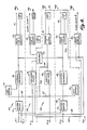
- branches or sectors 900 and 930 are essentially the same as one another from the standpoint of componentry, although having very definite operational differences to be noted subsequently.
- both branches 900 and 930 embody a control switch 10, 12, respectively, a reference control and threshold comparator set 14, 18 and 16, 22, respectively, and a driver, timer, and indicator unit or circuit portion 22 and 24, respectively, each of the latter having respective output terminals 21 and 25 as well as LED signal elements ("LED 2" and "LED 3", respectively).
- the respective outputs from the threshold comparators 18 and 22 are also directed to an integrator 34, and thus are seen to be summed with respect to one another; however, the particular manner in which such summing is carried out is an important aspect and is described in much greater detail hereinafter.
- the center circuit portion 920 includes an amplifying and integrating, or integrating detector, circuit portion 30, which receives an input from terminal DL-4 and has an output directed to a comparator and.alarm 32 having an LED indicator ("LED 1") as one of its outputs.
- the output from this alarm is also fed as an input to the lower circuit branch 940, more particularly, to a driver, timer and alarm unit 38, which as indicated provides an "Alarm Output No. 2".
- This same input terminal of the alarm unit 38 receives control signals on an input lead 39 connecting to the "signal gate” and "noise gate” inputs fed to control switches 10 and 12 from circuit input terminals DL-2 and DL-5.
- the second (upper) input terminal of the driver, timer and alarm unit 38 is coupled back to the input side of a discharge clamp 26 in path 910, whose primary input is from circuit terminal DL-3.
- the output of the discharge clamp 26 is coupled to, and directly affects, the integrator 34, and the integrator is coupled to, and actuates, a comparator, timer and alarm 28 having a primary alarm output directed to a lamp driver 29, which also provides a switched alarm output, labeled Alarm Output #1.
- timer and alarm 28 controls an indicator LED ("LED 4") coupled to its output.
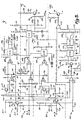
- the detector logic circuitry as depicted in Figs. 5 and 6, it will first be noted that the upper and lower portions of the circuit, comprising channels 900, 910, 930 and 940 in Fig. 4, are depicted in Fig. 5, whereas the central portion of the circuit, comprising the path designated by the numeral 920 in Fig. 4, is depicted separately in Fig. 6.
- the elements identified as “control switch 1" and “control switch 2" in Fig. 4, and designated by the numerals 10 and 12 therein, are shown to comprise input switching transistors Q1 and Q2, whose bases receive control inputs through resistors R8 and R9, respectively, from circuit input terminals DL-2 and DL-5.
- the bases of switching transistors Q, and Q2 are coupled together through resistors R4 and R10, and the junction of the latter two resistors is coupled to the low voltage side of a pull-up resistor R21, and then through conductor 39 to the positive or non- inverting side of an amplifier U 11 in path 940.
- the primary signal inputs to be switched by transistors Q1 and Q2 are received on circuit input terminal DL-1, which is coupled to the collector of each such transistor through resistors R6 and R5, respectively.
- the "reference control" components or units 14 and 16 of Fig. 4 are seen in Fig. 5 to comprise switches, e.g. transistors, Q4 and Q3, respectively, which are connected in emitter-follower configuration, and whose bases are coupled together by a lead 49 so as to receive a common input, to be described subsequently.
- switches e.g. transistors, Q4 and Q3, respectively, which are connected in emitter-follower configuration, and whose bases are coupled together by a lead 49 so as to receive a common input, to be described subsequently.
- the respective outputs from transistors Q4 and Q3 are coupled as reference inputs to threshold comparators U-1a and U-14a, and it is to be noted that the circuit arrangement of paths 900 and 930 is of an inverted configuration, i.e., the output from transistor Q4 in path 900 is applied as an inverting input to comparator U-1a, whereas the output from transistor Q3 in path 930 is applied to the non-inverting input of comparator U-14a.
- Each such comparator input also receives a particularly-set reference voltage obtained from the junction of voltage-divider resistors R14 and R1, and applied through input resistances R16 and R3, respectively.
- threshold comparators U-1a and U-14a receive inputs from the collectors of switching transistors Q1 and Q2, respectively. These inputs are also supplied to comparators U-1b and U-14b (which may be half of the same double integrated circuit amplifier comprising comparators U-1a and U-14a, respectively, for example, an integrated circuit comparator No. 339).
- the second comparators U-1 b and U-14b are used as drivers for ensuing timers and indicators U-2a and U-2b, whose primary function is merely to time out or an indicator drive signal of desired duration on respective signal lamps LED 2 and LED 3, as described hereinafter.
- the two timers U-2a and U-2b are interconnected to one another, and they may in fact be implemented as the complementary halves of an IC556 timer, which is a double unit.
- the lowermost circuit portion 940 of the detector logic network 9 comprises in effect a comparator, a current source which drives a ganged double-timer, and an amplified lamp-driver output for alarm signal purposes.
- the initial comparator comprises the aforementioned comparator unit U-11, which may be implemented by use of a 339 integrated circuit component.
- the comparator output is diode coupled to a transistor Q5 disposed in grounded- collector configuration to act as a timed current source whose timing cycle is determined by the charge rate on capacitor C14.
- This current source drives the double timer U-12a and U-12b, which may advantageously be the two halves of a No. 556 integrated circuit timer whose terminals are ganged in the manner illustrated.
- the first half of the timer, U-12a is diode-coupled (D7) to a final amplifier or driver U-13 and lamp driver Q6, driver U-13 being a further comparator component which may be implemented by use of a 339 IC whose non-inverting input is supplied by the same signal which is applied to the inverting side of the first-stage amplifier U-11.
- first timer stage U-12a is connected to (diode OR'd with) the second timer stage U-12b such that the first stage, upon its initial excitation, immediately commences a continuous lamp-driving operation of amplifier U-13 and switch Q6, as a "power on” indicator; however, whenever the current source comprising transistor Q5 and its timing capacitor C14 reaches full charge, the second timer (U-12b) is gated in and assumes control of the output signal, causing a blinking of the signal lamp driven by driver Q6, for purposes noted subsequently.
- Input terminal DL-1 receives the above-described output from the amp/filter 2, which as already pointed out comprises the arithmetically-summed antenna signals from both sides of a given portal, or group of portals, after band-pass amplification centered upon the fifteenth harmonic of the interrogation field fundamental frequency.
- This signal is supplied equally to the control switches Q1 and Q2, whose switching operation determines whether or not any portion of the supplied signal is gated through the switching transistors to either path 900 or path 930.
- the latter two channels are gated into and out of operation by timing signals applied to inputs DL-2 and DL-5, as supplied from the timing generator 4.
- the first such input, to transistor Q1, is representative of the "signal gate” or "marker signal window", i.e., those particular increments of time representing an increasing- current condition (both positive-going and negative-going) in the interrogation field drive coils; consequently, these gate signals represent times when a marker-present signal is likely to be present in the signals from the portal antennae, if a marker is in fact present within the interrogation field.
- the gating signals applied to terminal DL-5 and transistor Q2 represent the opposite portion of the interrogation field alternations, i.e., when marker-present signals are not likely to occur in the antennae signals even if a marker is present in the portal.
- the gate signals applied to terminal DL-5 define a "noise gate", i.e., a period of time during which the signals received by the portal antennae, on an instantaneous basis, represent an actual measure of the existing noise level in the antennae signals.
- the duration of the aforementioned “noise gate” is shorter than the duration of the “signal gate”, and that there is a gap or interval between the two. More particularly, assuming the interrogation field fundamental frequency to be 10 kHz, so that the duration of each quarter-cycle is 25 microseconds, the marker-present signals are likely to occur during the quarter-cycles when the current is increasing, either positively or negatively, whereas the current-decreasing quarter-cycles represent the condition when marker-present signals are not likely to occur in the antennae signals.
- timing generator By maintaining the "signal gate” for a full 25 microseconds but maintaining the "noise gate” for only approximately half that time, thus providing a gap of approximately 12 microseconds between each noise gate and ensuing signal gate, distortion and transients which otherwise would “ring through” the circuit will be eliminated, thus further enhancing sensitivity and reliability.
- the particular timing and synchronization of such signals are also highly important. While the general state of the art includes circuits and components well able to provide representative gating or blanking signals of this type, a preferred form of timing generator is a digital clock and divider, synchronized to the actual oscillation conditions of the interrogation field.
- circuit paths 900 and 930 of the detector logic 9 in effect alternate in operation, and during the period each is in operation it applies an input to the aforementioned threshold comparators U-1a (and U-1b) (in channel 900) and U-14a (and U-14b) (in channel 930).
- each such circuit path functions to alter the charge state of an integrating capacitor C9, and it is important to note that the two circuit paths act oppositely from one another in that regard.
- the switched input from transistor Q1 to comparator U-l in path 900 is applied to the noninverting (i.e., positive) input, whereas the opposite is true in path 930,- where the signals gated through by switch Q2 are applied to the inverting side of comparator U-14a. Consequently, the two such circuit paths act to rapidly and sequentially apply increments of charge to, and draw increments of charge from, integrating capacitor C9, on an alternating, increment-by-increment or pulse-by-pulse basis.
- circuit paths 900 and 930 note just above, that the signals gated through by transistors Q1 and Q2 to comparators U-1a and U-14a work against variable reference levels, and that these variable reference levels are applied to the opposite-polarity input terminal of each such comparator. That is, in circuit path 900 the inverting input of comparator U-1a receives the variable reference level, whereas in circuit path 930 it is the non-inverting input of comparator U-14a which receives the other such variable reference level. As already indicated above, these variable reference " levels both operate from the same nominal or steady-state reference level, obtained from the junction of voltage-divider resistors R14 and R1, through identical series resistors R16 and R3.
- This steady-state reference level is subject to variation, however, by the operation of transistors Q4 and Q3, which constitute the "reference controls" 14 and 16 noted in connection with Fig. 4. That is, in channel 900 the base of transistor Q4 is controlled, in a manner described more particularly hereinafter, so as to vary the resulting reference level applied to the inverting terminal of differential amplifier U-1a.
- the steady-state reference level is applied to the non-inverting input of comparator U-14a, and this nominal reference level is made subject to variation by reference control 16, i.e., transistor switch Q3, which receives the same varying input as transistor Q4, i.e., the base of each of these transistors is commonly coupled to receive the same control input signal (from the output of the amplifier, peak-detector and integrator 30 in path 920, shown in Fig. 5).
- the second-stage comparators U-1 and U-14b may be considered as in essence duplicative of the first such stage, insofar as inputs are concerned, except that instead of applying and subtracting charge from integrating capacitor C9, they are utilized to drive indicators LED 2 and LED 3, which are pulsed by timer units U-2a and U-2b, to indicate the operational status of each such circuit path.
- the second portion or channel 910 of the detector logic network 9 is also illustrated in detail in Fig. 5, and will be seen to include a pair of inputs, a first one of which is provided by circuit input terminal DL-3 which is coupled to the inverting input of a comparator U-3, comprising the "discharge clamp" -26 noted in connection with Fig. 4.
- the output of this comparator connects to the conductors 21 and 23 by which charge is applied to and removed from integrating capacitor C9. Therefore, when an appropriate gating signal is applied to the inverting side of comparator U-3, under general system conditions to be noted subsequently, this comparator/amplifier will clamp integrating capacitor C9 to ground, thus fully discharging the integrator.
- the detection logic and processor 9 involving that portion thereof designated generally as channel 910, and particularly of that portion of the circuitry disposed to the right of portal point 911, is the production of a desired alarm or signal upon the detected presence of the particular marker within the interrogation field. More particularly, it will be noted that the node or junction 911 where comparator U-3 interconnects with conductors 21 and 23, which lead to the integration capacitor C9, comprises the signal input to a comparator U-4, which receives a predetermined bias or steady-state reference on its positive (non-inverting) input terminal from voltage-divider resistors R13 and R15.
- timer U-5 (which may be an IC No. 555).
- One output of timer U-5 actuates an alarm signal (LED 4) and is also coupled to an output driver Q7, which may be used to drive a signal lamp, sound an audible alarm, or the like, utilizing an output taken at terminal 912 connected to the collector of transistor Q7.
- a switched output signal of timer U-5 which is representative of the control signal applied to the base of transistor Q7 is available on the output terminal designated 914.
- circuit path 910 receives an input on terminal DL-4, which input comprises the amplified, frequency-selective output from the inhibit amplifier 3, noted generally in connection with Fig. 1 and more particularly described in connection with Fig. 3.
- This signal from the inhibit amplifier 3 comprises sequential, time-gated, synchronized bursts of the subtracted (differenced) signals from the portal antennae, after low-pass selective amplification thereof in the inhibit amplifier. Consequently, this input to the detec- .
- tion logic circuit is representative of the low frequency component band (in the range of the third, fifth, and up to the seventh harmonic of the interrogation field, here on the order of 30 to 50, and approaching 70, kHz), which signal is attributable to an object within the interrogation field. Whether that object is an actual marker, or merely some non-marker element causing perturbations in the interrogation field, remains to be determined, but as already indicated, the true or actual markers will have a relatively unique ratio or balance of the high frequency component band with respect to the low frequency band.
- This low frequency band is used in the detection logic and processing unit 9 as a determinant which must be satisfied by the magnitude of the high frequency band produced by the same object within the interrogation field before a marker-present signal or alarm is sounded; i.e., the amount (magnitude) of the low frequency band actually encountered, as represented by the magnitude of the input applied to terminal DL-4, is used to determine the required level which the high frequency band produced by the same object in the field must equal or exceed if it is indeed an actual marker; the ratio or balance of these frequency components for true markers being relatively unique.
- the aforementioned input on terminal DL-4 is coupled to one end of a variable resistance or potentiometer R2, whose movable contact is coupled through a series resistor R56 to the inverting input of a differential amplifier U-6 coupled into the circuit as an inverting amplifier, whose gain is thus set by potentiometer R2.
- Inverting amplifier U-6 (which is preferably implemented by use of a 3240 integrated circuit operational amplifier) forms part of the amplifier, detector and integrator unit 30 noted briefly above in connection with Fig.
- inverting amplifier U-6 is diode-coupled through a series resistor R48 to the parallel combination of a second inverting amplifier U-7 and an R-C integrating network consisting of resistor R50 and capacitor C28.
- This overall network in effect comprises a combination amplifier, peak-detector and integrator, or in effect an integrating detector. That is, the charging time-constant for capacitor C28 is a function of the voltage drop across series resistor R48.
- capacitor C28 will build during the continuation of each burst of input signals applied to terminal DL-4 and passed by inverting amplifier U-6, with capacitor C28 integrating only the peaks of the negative excursions of the incoming signals (i.e., that portion of a cycle which exceeds the preset reference level).
- the peak-integration or integrating detector effect just noted is preferably accomplished by maintaining the integration time constant or capacitor C28 of very short duration, for example by utilizing a .1 microfarad capacitor for C28 and a 4.6 K-ohm resistor for R48.
- This will produce a very fast-acting integrator which will operate in the manner of a current source, i.e., integrating for only the first few excursions and tracking the applied signal very. accurately and closely, yet reducing the effects of narrow, high-amplitude spikes due to switching transients from the blanking (gate-generating) and other related circuitry.
- This type of detector is preferred since the band-pass stages preceding it allow some of the higher order components (for example in the range of 140 kHz) to pass through, usually in the form of spikes. Additionally, spikes may be created by the blanking circuitry, as just indicated. If a more conventional peak-detector was used, such spikes would result in a high level of detected signal, whereas the preferred integrating detector responds more to the average value above the diode (D-10) voltage drop.
- D-10 diode
- the level of the signal so integrated appears on conductor 48, on the output side of inverting amplifier U-7, and this signal level is not only coupled forward to a comparator .U-8, but is also reflected back (on conductors 50, 47 and 49) as a threshold-changing signal to transistors Q3 and Q4, (i.e., "reference controls" 14 and 16) noted above in connection with Figs. 4 and 5.
- comparator U-8 The forwardly-coupled signal from inverting amplifier U-7 is applied to comparator U-8 and, when this signal rises to a predetermined level constituting a system override condition, comparator U-8 switches, thereby energizing an indicator labeled "LED 1", through a series resistance R52 and a level-setting resistor R53. This provides a visual indication that the charge level on integrating capacitor C28 has reached the override threshold voltage determined by comparator U-8. Furthermore, the output of comparator U-8 is coupled to the inverting input of differential amplifier U-9, to whose output is also coupled the anode side of LED 1, and the resulting output from amplifier U-9 is coupled to one input of a second inverting amplifier U-10.
- amplifier U-10 is coupled back, on conductor 901, to the non-inverting input of the aforementioned amplifier U-11 in path 940 (Fig. 5), whose function has been described previously, and also coupled back (on conductor 39) to the bases of switching transistors Q1 and Q2, to bring about system override, or lockout, as will be noted subsequently.
- the input to terminal DL-4 of channel 920 representing the lower-frequency spectrum produced by the interrogation field-monitoring antennae, is utilized, with appropriate processing, to accomplish two distinct purposes.
- the peak- detected and integrated reflection of this input is coupled back to the bases of threshold reference- setting transistors Q3 and Q4, to change the threshold level of comparators U-1a and U-14a as a direct function of the instantaneous level of the low frequency spectrum produced by an object detected in the portals.
- the effect of this is to change in a very significant way the amounts of charge applied to and accumulated on integrating capacitor C9.
- the present detection system provides a multiple-step or multilayered approach for highly sensitive and yet highly selective detection of the low-coercivity permalloy or other such marker within the interrogation field, based upon the inevitably characteristic and relatively unique balance or ratio of low-order harmonics versus high-order harmonics caused by the magnetic domain-switching of the marker in response to each ensuing half-cycle of alternation of the interrogation field.
- the higher-frequency harmonic band will be deficient in objects and articles which are not true markers, even through in a general sense substantial quantities of the higher-order harmonics may indeed be present, particularly in objects and articles which provide multiple magnetic paths or loops and which include at least some arcing points, i.e., gaps in the magnetic circuits.
- the invention provides a method and means to determine the low-frequency components or band and the high-frequency components or band of an object within the interrogation field, and these low frequency components are used to dynamically control the detection threshold of the high-frequency components which produce an alarm signal.
- the signals from the antennae monitoring the interrogation field are carefully processed to produce two different types of signal output: one which represents the summation of the signals from the antennae, for maximum sensitivity, and the other of which represents the differencing of the signals from opposite sides of the interrogation field, for maximum selectivity.
- condition just described indicative of an unusual and undesirable situation prevalent within the interrogation field which is causing a substantial overbalancing of the detection circuitry by way of excessive levels of the low-frequency harmonic band, is a severe aberration in the detection circuit parameters, and thus indicates the advisability of fully inhibiting the detection circuitry, in addition to the flashing lamp indication just noted which shows the existence of the condition.
- the signal indicative of the low-frequency overbalance which is coupled back to channel 940 for the purpose of enabling and driving the flashing lamp indicator is also coupled back, on conductor 39, to each of the control switches 10 and 12 (transistors Q1 and Q2) such that they latch out and block the input from terminal DL-1, thereby preventing any build-up on integrator 34 (capacitor C9) which might otherwise result in an erroneous detection alarm.
- the level of the instantaneously-variable detection threshold or reference on comparators U-1a and U-14a set initially by voltage divider R14 and R1, and varied by proportional or relative conduction of transistors Q3 and Q4, is in effect stored for a short time interval on capacitors C7 and C8, coupled to the emitters of transistors Q4 and Q3, respectively, through a time constant-setting resistor R16 and R3, respectively.
- the peak levels of threshold variation due to conductance of transistors Q3 and Q4 in response to elevated inhibit signals from integrating capacitor C28 are stored on capacitors C7 and C8 between phases; thus, these threshold peaks will be held briefly when the interrogation field switches its resultant flux direction in response to reversal in the phase of the drive excitation applied to one of the interrogation field-inducing coils.
- the system will not be susceptible to error as a result of detection harmonic content levels which vary substantially from one phase condition to the next.
- What is desired is to have enough storage in the system so that relatively high inhibit levels built up during one phase condition, which have effectively raised the threshold at the comparators to a substantial degree, will be maintained after the change in phase condition for at least the first half-cycle of the next interrogation field alternation and resulting detection signal, representative of a change in phase condition.
- the interrogation field fundamental frequency to be the aforementioned 10 kHz
- a bleed-off time constant on the order of about 100 msec for capacitors C7 and C8 (the combined resistance of resistors R16 and R1 for C7 and R3 and R1 for C8)
Landscapes
- Physics & Mathematics (AREA)
- Engineering & Computer Science (AREA)
- Automation & Control Theory (AREA)
- Computer Security & Cryptography (AREA)
- Electromagnetism (AREA)
- General Physics & Mathematics (AREA)
- Burglar Alarm Systems (AREA)
- Geophysics And Detection Of Objects (AREA)
Claims (37)
Priority Applications (1)
| Application Number | Priority Date | Filing Date | Title |
|---|---|---|---|
| AT83901292T ATE45231T1 (de) | 1982-03-15 | 1983-03-10 | Verfahren und vorrichtung fuer diebstahlaufspuersysteme. |
Applications Claiming Priority (6)
| Application Number | Priority Date | Filing Date | Title |
|---|---|---|---|
| US358383 | 1982-03-15 | ||
| US06/358,299 US4535323A (en) | 1982-03-15 | 1982-03-15 | Preamplifying and signal processing method and apparatus for theft detection systems |
| US06/358,383 US4524350A (en) | 1982-03-15 | 1982-03-15 | Detection logic and signal processing method and apparatus for theft detection systems |
| US36426482A | 1982-04-01 | 1982-04-01 | |
| US358299 | 1994-12-19 | ||
| US364264 | 1994-12-27 |
Publications (3)
| Publication Number | Publication Date |
|---|---|
| EP0103629A1 EP0103629A1 (fr) | 1984-03-28 |
| EP0103629A4 EP0103629A4 (fr) | 1987-03-12 |
| EP0103629B1 true EP0103629B1 (fr) | 1989-08-02 |
Family
ID=27408345
Family Applications (1)
| Application Number | Title | Priority Date | Filing Date |
|---|---|---|---|
| EP83901292A Expired EP0103629B1 (fr) | 1982-03-15 | 1983-03-10 | Procede et appareil pour systemes de detection de vols |
Country Status (5)
| Country | Link |
|---|---|
| EP (1) | EP0103629B1 (fr) |
| AU (1) | AU562133B2 (fr) |
| CA (1) | CA1217256A (fr) |
| DE (1) | DE3380326D1 (fr) |
| WO (1) | WO1983003203A1 (fr) |
Families Citing this family (5)
| Publication number | Priority date | Publication date | Assignee | Title |
|---|---|---|---|---|
| US4668942A (en) * | 1984-11-19 | 1987-05-26 | Progressive Dynamics, Inc. | Signal analysis apparatus including recursive filter for electromagnetic surveillance system |
| US4888579A (en) * | 1988-09-16 | 1989-12-19 | Minnesota Mining And Manufacturing Company | False alarm minimization and direction determination methods |
| US5748086A (en) * | 1995-11-14 | 1998-05-05 | Sensormatic Electronics Corporation | Electronic article surveillance system with comb filtering and false alarm suppression |
| GB9915595D0 (en) * | 1999-07-02 | 1999-09-01 | Sadler Robin W | Identification apparatus for reading moving tags in passageways |
| JP2009509426A (ja) | 2005-09-20 | 2009-03-05 | オールフレックス・オーストラリア・プロプライエタリー・リミテッド | ポータルアンテナ |
Family Cites Families (10)
| Publication number | Priority date | Publication date | Assignee | Title |
|---|---|---|---|---|
| FR763681A (fr) * | 1933-11-10 | 1934-05-04 | Procédé de repérage des objets par modification d'un champ magnétique | |
| US3747086A (en) * | 1968-03-22 | 1973-07-17 | Shoplifter International Inc | Deactivatable ferromagnetic marker for detection of objects having marker secured thereto and method and system of using same |
| US3665449A (en) * | 1969-07-11 | 1972-05-23 | Minnesota Mining & Mfg | Method and apparatus for detecting at a distance the status and identity of objects |
| US3740742A (en) * | 1971-05-11 | 1973-06-19 | T Thompson | Method and apparatus for actuating an electric circuit |
| US3838409A (en) * | 1973-04-13 | 1974-09-24 | Knogo Corp | Field strength uniformity control system for article theft detection system |
| US3983552A (en) * | 1975-01-14 | 1976-09-28 | American District Telegraph Company | Pilferage detection systems |
| US4168496A (en) * | 1977-10-05 | 1979-09-18 | Lichtblau G J | Quasi-stationary noise cancellation system |
| US4300183A (en) * | 1980-03-27 | 1981-11-10 | Richardson Robert H | Method and apparatus for generating alternating magnetic fields to produce harmonic signals from a metallic strip |
| US4321586A (en) * | 1980-08-21 | 1982-03-23 | Knogo Corporation | Article theft detection |
| US4309697A (en) * | 1980-10-02 | 1982-01-05 | Sensormatic Electronics Corporation | Magnetic surveillance system with odd-even harmonic and phase discrimination |
-
1983
- 1983-03-10 EP EP83901292A patent/EP0103629B1/fr not_active Expired
- 1983-03-10 AU AU14719/83A patent/AU562133B2/en not_active Ceased
- 1983-03-10 WO PCT/US1983/000316 patent/WO1983003203A1/fr not_active Ceased
- 1983-03-10 DE DE8383901292T patent/DE3380326D1/de not_active Expired
- 1983-03-14 CA CA000423477A patent/CA1217256A/fr not_active Expired
Also Published As
| Publication number | Publication date |
|---|---|
| AU1471983A (en) | 1983-10-24 |
| WO1983003203A1 (fr) | 1983-09-29 |
| EP0103629A4 (fr) | 1987-03-12 |
| AU562133B2 (en) | 1987-05-28 |
| EP0103629A1 (fr) | 1984-03-28 |
| CA1217256A (fr) | 1987-01-27 |
| DE3380326D1 (en) | 1989-09-07 |
Similar Documents
| Publication | Publication Date | Title |
|---|---|---|
| US5103234A (en) | Electronic article surveillance system | |
| CA1294342C (fr) | Systeme de surveillance d'articles electroniques | |
| AU606295B2 (en) | False alarm minimization and direction determination methods | |
| AU686341B2 (en) | Metal detection system | |
| CN105842739B (zh) | 通过式特定金属探测门 | |
| EP0130286B1 (fr) | Procédé et appareil pour détecter des éléments indicateurs dans une zone de surveillance | |
| EP1502244B1 (fr) | Systeme electronique de surveillance d'articles | |
| US4476459A (en) | Theft detection method and apparatus in which the decay of a resonant circuit is detected | |
| CA1069603A (fr) | Systemes de detection de griveleries | |
| CA2091790A1 (fr) | Methode et systeme de surveillance electromagnetique pour zone de securite | |
| US4206451A (en) | Intrusion detection system | |
| JPH08507624A (ja) | 電子的物品保護システム | |
| GB2154396A (en) | Security tag detection system | |
| US4524350A (en) | Detection logic and signal processing method and apparatus for theft detection systems | |
| JPH11503254A (ja) | 適応フィルタリングおよびデジタル検出を用いた電子物品監視システム | |
| EP0646266B1 (fr) | Systeme de detection de vol faisant appel au traitement de signaux numeriques | |
| US4535323A (en) | Preamplifying and signal processing method and apparatus for theft detection systems | |
| AU562133B2 (en) | Method and apparatus for theft detection systems | |
| AU711993B2 (en) | Electronic article surveillance system with comb filtering by polyphase decomposition and nonlinear filtering of subsequences | |
| GB2247383A (en) | Antenna array for an electronic article surveillance system | |
| CA1229896A (fr) | Logique de detection et methode et appareil de traitement de signal pour antivol | |
| DE3049140A1 (de) | Einrichtung zur anzeige des vorhandenseins von aus magnetisierbarem material bestehenden sicherungsstreifen in einem ueberwachungsbereich |
Legal Events
| Date | Code | Title | Description |
|---|---|---|---|
| PUAI | Public reference made under article 153(3) epc to a published international application that has entered the european phase |
Free format text: ORIGINAL CODE: 0009012 |
|
| AK | Designated contracting states |
Designated state(s): AT BE CH DE FR GB LI LU NL SE |
|
| 17P | Request for examination filed |
Effective date: 19840221 |
|
| A4 | Supplementary search report drawn up and despatched |
Effective date: 19870312 |
|
| 17Q | First examination report despatched |
Effective date: 19880229 |
|
| GRAA | (expected) grant |
Free format text: ORIGINAL CODE: 0009210 |
|
| AK | Designated contracting states |
Kind code of ref document: B1 Designated state(s): AT BE CH DE FR GB LI LU NL SE |
|
| REF | Corresponds to: |
Ref document number: 45231 Country of ref document: AT Date of ref document: 19890815 Kind code of ref document: T |
|
| REF | Corresponds to: |
Ref document number: 3380326 Country of ref document: DE Date of ref document: 19890907 |
|
| ET | Fr: translation filed | ||
| PLBE | No opposition filed within time limit |
Free format text: ORIGINAL CODE: 0009261 |
|
| STAA | Information on the status of an ep patent application or granted ep patent |
Free format text: STATUS: NO OPPOSITION FILED WITHIN TIME LIMIT |
|
| 26N | No opposition filed | ||
| PGFP | Annual fee paid to national office [announced via postgrant information from national office to epo] |
Ref country code: FR Payment date: 19911227 Year of fee payment: 10 |
|
| PGFP | Annual fee paid to national office [announced via postgrant information from national office to epo] |
Ref country code: GB Payment date: 19920213 Year of fee payment: 10 |
|
| PGFP | Annual fee paid to national office [announced via postgrant information from national office to epo] |
Ref country code: AT Payment date: 19920219 Year of fee payment: 10 |
|
| PGFP | Annual fee paid to national office [announced via postgrant information from national office to epo] |
Ref country code: SE Payment date: 19920221 Year of fee payment: 10 |
|
| PGFP | Annual fee paid to national office [announced via postgrant information from national office to epo] |
Ref country code: CH Payment date: 19920327 Year of fee payment: 10 |
|
| PGFP | Annual fee paid to national office [announced via postgrant information from national office to epo] |
Ref country code: DE Payment date: 19920330 Year of fee payment: 10 |
|
| PGFP | Annual fee paid to national office [announced via postgrant information from national office to epo] |
Ref country code: NL Payment date: 19920331 Year of fee payment: 10 |
|
| PGFP | Annual fee paid to national office [announced via postgrant information from national office to epo] |
Ref country code: BE Payment date: 19920409 Year of fee payment: 10 |
|
| PGFP | Annual fee paid to national office [announced via postgrant information from national office to epo] |
Ref country code: LU Payment date: 19921231 Year of fee payment: 10 |
|
| EPTA | Lu: last paid annual fee | ||
| PG25 | Lapsed in a contracting state [announced via postgrant information from national office to epo] |
Ref country code: LU Free format text: LAPSE BECAUSE OF NON-PAYMENT OF DUE FEES Effective date: 19930310 Ref country code: GB Effective date: 19930310 Ref country code: AT Effective date: 19930310 |
|
| PG25 | Lapsed in a contracting state [announced via postgrant information from national office to epo] |
Ref country code: SE Effective date: 19930311 |
|
| PG25 | Lapsed in a contracting state [announced via postgrant information from national office to epo] |
Ref country code: LI Effective date: 19930331 Ref country code: CH Effective date: 19930331 Ref country code: BE Effective date: 19930331 |
|
| BERE | Be: lapsed |
Owner name: PROGRESSIVE DYNAMICS INC. Effective date: 19930331 |
|
| PG25 | Lapsed in a contracting state [announced via postgrant information from national office to epo] |
Ref country code: NL Effective date: 19931001 |
|
| GBPC | Gb: european patent ceased through non-payment of renewal fee |
Effective date: 19930310 |
|
| NLV4 | Nl: lapsed or anulled due to non-payment of the annual fee | ||
| PG25 | Lapsed in a contracting state [announced via postgrant information from national office to epo] |
Ref country code: FR Effective date: 19931130 |
|
| REG | Reference to a national code |
Ref country code: CH Ref legal event code: PL |
|
| PG25 | Lapsed in a contracting state [announced via postgrant information from national office to epo] |
Ref country code: DE Effective date: 19931201 |
|
| REG | Reference to a national code |
Ref country code: FR Ref legal event code: ST |
|
| EUG | Se: european patent has lapsed |
Ref document number: 83901292.9 Effective date: 19931008 |