EP0104290B1 - Digitalprozessor für Echtzeitsignale - Google Patents
Digitalprozessor für Echtzeitsignale Download PDFInfo
- Publication number
- EP0104290B1 EP0104290B1 EP82401768A EP82401768A EP0104290B1 EP 0104290 B1 EP0104290 B1 EP 0104290B1 EP 82401768 A EP82401768 A EP 82401768A EP 82401768 A EP82401768 A EP 82401768A EP 0104290 B1 EP0104290 B1 EP 0104290B1
- Authority
- EP
- European Patent Office
- Prior art keywords
- bus
- input
- memory
- address
- output
- Prior art date
- Legal status (The legal status is an assumption and is not a legal conclusion. Google has not performed a legal analysis and makes no representation as to the accuracy of the status listed.)
- Expired
Links
Images




Classifications
-
- G—PHYSICS
- G06—COMPUTING OR CALCULATING; COUNTING
- G06F—ELECTRIC DIGITAL DATA PROCESSING
- G06F15/00—Digital computers in general; Data processing equipment in general
- G06F15/76—Architectures of general purpose stored program computers
- G06F15/80—Architectures of general purpose stored program computers comprising an array of processing units with common control, e.g. single instruction multiple data processors
- G06F15/8007—Architectures of general purpose stored program computers comprising an array of processing units with common control, e.g. single instruction multiple data processors single instruction multiple data [SIMD] multiprocessors
Definitions
- the present invention relates to a digital real-time signal processor. It finds applications in sound processing, in telecommunications, in image processing, in process control optimization, etc ... and more generally in all real-time signal processing techniques.
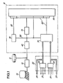
- FIG. 1 A computer 10 is connected to a mass memory 12 and to dialogue members 14. This computer is associated with a peripheral processor 16.
- This processor includes all firstly, an input-output circurt 20; some inputs 21 are provided with an analog-to-digital converter 22 and others, 23, with an analog-to-digital converter 24. These input-outputs therefore work in analog.
- the other inputs 25 and outputs 26 work in digital.
- the peripheral processor further comprises an input-output management unit 30, a circuit 40 for coupling with the computer 10, a buffer memory 50, digital processing means 60 and a circuit 70 for managing the means 60. The all of these means are interconnected by a bus 80.
- the computer 10 manages the peripheral processor 16.
- the mass memory 12 stores information intended for the processor or coming from the latter.
- Signals from outside can be applied to the inputs 21, 25.
- signals delivered by the outputs 23, 26 can be applied to external means which are not shown and whose nature naturally depends on the application in progress.
- Digital real-time signal processors intended to be coupled to a computer and to an input-output unit via an input-output circuit are known from the documents ELECTRONIC DESIGN, volume 30, number 11, May 1982, pages 153 -158 and Implementing functions: microprocessors and firmware, seventh EUROMICRO symposium on microprocessing and microprogramming, Paris, September 8-10, 1981, edited by L. Richter, P. Le Beux, G. Chroust, G. Noguez, North-Holland Publishing Company-Amsterdam, New-York, Oxford, pages 455-463.
- the digital signal processing means consist of a single module which comprises an arithmetic unit containing a fast multiplier, a shift register, a function memory, a data memory, an address memory, and a firmware memory.
- the digital signal processing means consist of a plurality of interconnected processing modules.
- Such processors include digital processing means, the various elements of which have a configuration determined in advance and which is a function of the processing to be carried out. If this solution is well suited when this treatment is always the same, it naturally has a disadvantage when it comes to performing different operations, which may vary during treatment, or from one treatment to another.
- the present invention solves this problem by proposing processing means composed of elements capable of being organized in various configurations. These are controlled by firmware which is stored in a special memory.
- the invention therefore relates essentially to a processor such as the assembly 16 of FIG. 1 and more particularly to the structure and the function of the means 60 of the system belonging to this processor.
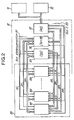
- FIG. 2 schematically represents the practical organization of the circuits of the processor and specifies the links between these circuits.
- the processor comprises eight identical processing cards, referenced from 101 to 108, the assembly forming a processing means 60.
- the buffer memory 50 is arranged on a ninth card 109.
- the input-output management unit 30 as well as the management circuit 70 are grouped on an additional card 110.
- the circuit 40 for coupling with the computer is arranged on an eleventh card 111.
- the processing cards 101 to 108 as well as the cards 109 and 110 are connected by an interconnection bus 81 composed of a receiving bus 82, a transmitting bus 83 and a data bus 84. Furthermore, all the cards are linked by a system bus 85 (bus S) composed of a selection bus 86, an address bus 87, a waveform address bus 88 and a bus 85.
- bus S system bus 85
- the data is conveyed by the bidirectional data bus 89.
- the waveform memories of the processing cards are addressed by the address bus 88 originating from a particular logic installed in the card 50.
- An example from the electro-acoustic domain can be given: after having obtained an orchestral configuration, the programming defining it can be memorized with a view to its reuse. On the other hand, the work produced can also be stored in the form of data. A work thus prerecorded can serve as basic data for further processing.
- the clock circuits are programmable counters which make it possible to determine time intervals at the end of which a request for intervention to the computer (interruption) obliges him to suspend the task which he was performing, in order to modify elements of the processing. running in the processor.
- the main applications of clock circuits are, the development of envelopes for the evolution of the amplitudes and frequencies of the oscillators, the evolution of the filter cut-off frequencies, etc. ..
- the arbitration logic allows the transfer of data between a card and others among the eight processing cards, the memory card 50 and the card 110 itself, this via the interconnection bus 81.
- the interconnections to be performed are specified by the content of a memory of 512 words of 14 bits previously loaded by the computer.
- the input-output management unit manages communication with the outside, either in digital form (inputs 25, outputs 26 in FIG. 1), or in analog form (inputs 21, outputs 23); in this case, it supports the management of analog-digital and digital-analog converters placed outside.
- the interface card 40 performs the conventional coupling function between the processor and the chosen computer. Part of it is invariant, since it creates the system bus 85, while another part is specific to the computer used and therefore must change with it.
- Each card communicates with the computer and its periphery via the card 40, using the system bus 85, either directly or via a buffer memory. It can also exchange the information processed with the other cards via the interconnection bus 81.
- the functional structure of the processing card is illustrated in FIG. 3.
- the functional elements communicate with each other via a bus A and a bus B according to a structure called "pipeline".
- This structure increases the processing speed. It consists of a series of sections, each responsible for carrying out part of the processing, the information succeeding one another in the sections as a fluid does in a pipe.
- All of these elements, interconnected according to the current firmware, can exchange information (data or addresses) with the other cards of the system, via the interconnection bus 81 or with the outside via the system bus 85.
- Figures 4, 5, 6, 8, 9 represent some of the basic structures most used in signal processing. Each of these structures makes it possible to carry out several types of treatment.
- FIG. 4 first of all shows a multiplier 120 with two inputs e 1 and e 2 , an arithmetic unit 115 of which an input e 3 is connected to the multiplier 120 and of which another input is denoted e4. This unit delivers a signal on an output s.
- the input e 1 receives a number a i , the input e 2 a unitary signal 1, and the input e4 a number b i .
- the output then delivers a sum signal:
- the inputs e 1 and e 2 receive numbers a and b i , and the input e4 is connected to the output s.
- the input e 1 is looped back to the output s, the input e 2 receives a signal x, and the input e4 a signal a i .
- the output signal is of the form: which allows the calculation of polynomials by the recurrent formula:
- FIG. 6 illustrates a configuration involving the arithmetic unit 115 which works with three inputs e 3 , e4, e5 and the waveform memory 140.
- the latter contains samples of the functions to be reproduced.
- This memory includes a selection entry e 6 and a second entry e 7 which corresponds to an address. This input is connected to the output s of the unit 115.
- the memory 140 also has an output t.
- a particular waveform is obtained, on the one hand by choosing an appropriate signal on the input e 6 and, on the other hand, by sequentially exploring the memory in order to place on the output t the series of corresponding samples.
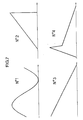
- Figure 7 shows four possible functions.
- the exploration mode determines the temporal occurrence of the waveform.
- a simple incrementation of the address of memory 140 will make appear, in the case of wave n ° 1, a sinusoid whose frequency is linked to the increment (the larger the increment, the higher the frequency is high).
- a variable increment allows frequency modulation.
- the initial phase ⁇ i (input e 3 ), the frequency F (input e4), the frequency step ⁇ F (input e 5 ) and the parameters of the frequency modulation can be presented.
- the output s delivering ⁇ i + 1 is looped back to the input e 3 .
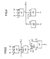
- FIG. 8 corresponds to that of FIG. 6 (arithmetic unit 115 and memory of waveforms 140) with, in addition, a multiplier 120 connected to the output of memory 140. Furthermore, this multiplier receives on its input e 2 a signal A enabling amplitude modulation to be obtained.
- the output signal denoted SS, delivered by the multiplier 120 can be mixed with another signal, denoted SS 2 , by a second arithmetic unit 115 'receiving these two signals on its inputs e' 3 and e ' s .
- FIG. 9 represents a variant in which the circuit of FIG. 6 is completed by the shift register 130, the input e 8 of which is connected to the output s of the unit 115.
- This circuit makes it possible to perform linear interpolation using the least significant bits, (below the 16th, for example, for 24 bits handled during the calculation).
- an elementary instruction cycle, or microcycle has a duration of 61.035 ns.
- the memory of the firmware delivers a microinstruction which establishes the functional configuration corresponding to the action executed during this microcycle.
- the operands on which the microinstructions work have their addresses in the address memory 160.
- the 32 microinstructions, corresponding to the 32 words of the microprogram memory 180, form an intermediate cycle of duration 1.95 ⁇ s.
- the firmware in a complete cycle of duration 62.5 They are executed 32 times with different data, which implies that the address memory 160 has a size of 32 ⁇ 32 words, or 1024 words.
- the organization of this memory is illustrated in FIG. 10.
- the 32 blocks of memory 160 are referenced respectively: A o for that which contains the addresses relating to cycle 0, A 1 for that which contains the addresses relating to cycle 1, etc ... and A 31 for the last.
- FIG. 11 includes three time diagrams: the first, a, represents the clock pulses of HMP firmware, the second, b, the addresses explored in the firmware memory 180, ie AuP , and the third, c, the addresses of the address memory 160, namely AMA.
- the signal processing sampling period is 62.5 ⁇ s in this case, i.e. a sampling frequency of 16000 Hz, which corresponds to a processed signal bandwidth of 8000 Hz. (Shannon's theorem shows that the maximum bandwidth of a sampled signal is half the sampling frequency).
- microcycle used must be repeated within the complete cycle.
- E is an input we can show that S is an output corresponding to a low-pass filtering, an output corresponding to bandpass filtering, and an output corresponding to high pass filtering.
- the letter ro denotes a tuning pulse and Q denotes an overvoltage coefficient.
- This equation can be solved from the analog circuit of Figure 12a.
- This circuit includes two integrators 201 and 202, two multipliers 203 and 204 and an adder-subtractor 205 with three inputs.
- the input quantities are the signals 8, applied to the multiplier 203, ⁇ 2 to the multiplier 204 and E to a positive input of the adder-subtractor 205.
- the integrators can be produced numerically using adders-accumulators by a simple loopback, which leads to the diagram of FIG. 12b which solves the equation: more suitable for providing the three desired outputs.
- the circuit shown comprises four multipliers 211, 212, 213 and 214 and four adders 221, 222, 223 and 224. This diagram can be produced using the functional element of FIG. 4 and leads to the diagram of FIG. 12c which includes four sets 231, 232, 233 and 234.
- a card brings together the equivalent of 128 independent oscillators with two frequency inputs. By using eight similar cards, it is possible to have 1024 oscillators.
- One card represents the equivalent of 224 multiplier-adders (32 cycles of seven multiplier-adders) that can realize up to 56 second-order filters.
- This operation involves about a quarter of the card, the remaining part being able to perform other operations.
- interconnection software There may be several versions of this software, called interconnection software, which are intended for separate users. Some remain close to the equipment (use of the quantities in octal, definition of the memories used, etc ). others want to ignore the machine (use of names of mnemonic variables, introduction of frequencies in RH, etc ).
- the processor of the invention has the following characteristics: it is an intelligent and autonomous device.
- the h * ote computer can be used for other tasks, such as the management of the operating modes of the system, or any preparatory treatment not being carried out in real time, the real-time treatments being entirely supported by the processor.
Landscapes
- Engineering & Computer Science (AREA)
- Computer Hardware Design (AREA)
- Theoretical Computer Science (AREA)
- Computing Systems (AREA)
- Physics & Mathematics (AREA)
- General Engineering & Computer Science (AREA)
- General Physics & Mathematics (AREA)
- Complex Calculations (AREA)
Claims (1)
ein Pufferspeicher (50),
wobei dieser Prozessor dadurch gekennzeichnet ist, daß jeder Modul umfaßt:
Priority Applications (2)
| Application Number | Priority Date | Filing Date | Title |
|---|---|---|---|
| EP82401768A EP0104290B1 (de) | 1982-09-29 | 1982-09-29 | Digitalprozessor für Echtzeitsignale |
| DE8282401768T DE3277851D1 (en) | 1982-09-29 | 1982-09-29 | Digital processor for real time signals |
Applications Claiming Priority (1)
| Application Number | Priority Date | Filing Date | Title |
|---|---|---|---|
| EP82401768A EP0104290B1 (de) | 1982-09-29 | 1982-09-29 | Digitalprozessor für Echtzeitsignale |
Publications (2)
| Publication Number | Publication Date |
|---|---|
| EP0104290A1 EP0104290A1 (de) | 1984-04-04 |
| EP0104290B1 true EP0104290B1 (de) | 1987-12-16 |
Family
ID=8189940
Family Applications (1)
| Application Number | Title | Priority Date | Filing Date |
|---|---|---|---|
| EP82401768A Expired EP0104290B1 (de) | 1982-09-29 | 1982-09-29 | Digitalprozessor für Echtzeitsignale |
Country Status (2)
| Country | Link |
|---|---|
| EP (1) | EP0104290B1 (de) |
| DE (1) | DE3277851D1 (de) |
Families Citing this family (2)
| Publication number | Priority date | Publication date | Assignee | Title |
|---|---|---|---|---|
| GB2152249B (en) * | 1983-12-26 | 1987-09-09 | Mitsubishi Electric Corp | Video signal processor |
| IT1182575B (it) * | 1985-09-27 | 1987-10-05 | Elsag | Sistema per realizzare elaborazioni convolutive veloci su informazioni rappresentative di immagini |
-
1982
- 1982-09-29 EP EP82401768A patent/EP0104290B1/de not_active Expired
- 1982-09-29 DE DE8282401768T patent/DE3277851D1/de not_active Expired
Non-Patent Citations (1)
| Title |
|---|
| Implementing functions: microprocessors and firmware, seventh EUROMICRO symposium on microprocessing and microprogramming, Paris, Septembre 8-10, 1981, edited by L. Richter, P. Le Beux, G. Chroust, G. Noguez, North-Holland Publishing Company-Amsterdam, New York, Oxford, pages 455-463 * |
Also Published As
| Publication number | Publication date |
|---|---|
| DE3277851D1 (en) | 1988-01-28 |
| EP0104290A1 (de) | 1984-04-04 |
Similar Documents
| Publication | Publication Date | Title |
|---|---|---|
| EP0046708B1 (de) | Digitale Signalverarbeitungsschaltung in verteilter Arithmetik mit Verwendung eines Multiplexers am Eingang eines Speichers | |
| EP0207859B1 (de) | Rechnungseinrichtung zur diskreten und verschiebenden Fourier-Transformation zur Verwendung in einem Radarsystem | |
| EP0926823B1 (de) | Programmierbare Schaltung zur Realisierung eines digitalen Filters | |
| EP0171305B1 (de) | Rechenschaltung für die diskrete Fouriertransformation | |
| EP0223657A1 (de) | Rechnungseinrichtung von diskreter Fouriertransformation und seine Anwendung auf einem Radarsystem | |
| US6018754A (en) | Apparatus for filtering a signal utilizing recursion and decimation | |
| EP0275765B1 (de) | Integrierter Schaltkreis für Digitalsignalverarbeitung | |
| FR2714549A1 (fr) | Filtre numérique et convertisseur analogique-numérique à suréchantillonnage employant ce filtre. | |
| EP0437876A1 (de) | Programmierbarer serieller Multiplikator | |
| EP0022513B1 (de) | Gerät zur Berechnung der zweidimensionalen diskreten Fouriertransformation | |
| US4554629A (en) | Programmable transform processor | |
| US4627026A (en) | Digital real-time signal processor | |
| EP0104290A1 (de) | Digitalprozessor für Echtzeitsignale | |
| FR2747528A1 (fr) | Structure de dispositif de banc de filtres numeriques et son procede de fonctionnement | |
| GB2103005A (en) | Modulation effect device | |
| EP0327445A1 (de) | Allgemeiner digitaler Multiplizierer und digitaler Filter mit diesem Multiplizierer | |
| FR2511169A1 (fr) | Processeur numerique de signal en temps reel | |
| EP0476592A2 (de) | Adressengenerator für den Datenspeicher eines Prozessors | |
| EP0043745B1 (de) | Digitales Datenverarbeitungs- und Speichersystem, insbesondere für ein Tomodensitometer | |
| EP0190514B1 (de) | On-line-Testeinrichtung für einen Rechnerkreis der diskreten Fouriertransformation und Kreis der eine solche Einrichtung enthält | |
| EP0011576B1 (de) | Polyphone Syntheseschaltung für periodische Signale unter Anwendung digitaler Techniken | |
| EP0242258A1 (de) | Vorrichtung zur Durchführung eines Algorithmus (Leroux-Gueguen) zum Codieren eines Signals durch Linearvorhersage | |
| EP0718746B1 (de) | Booth-Multiplizierer für trigonometrische Funktionen | |
| EP1218820B1 (de) | Verfahren zur automatischen anordnung der aufgaben einer anwendung in einer signalverarbeitungsmaschine | |
| Slump et al. | Design and implementation of a linear-phase equalizer in digital audio signal processing |
Legal Events
| Date | Code | Title | Description |
|---|---|---|---|
| PUAI | Public reference made under article 153(3) epc to a published international application that has entered the european phase |
Free format text: ORIGINAL CODE: 0009012 |
|
| AK | Designated contracting states |
Designated state(s): BE CH DE GB IT LI LU NL |
|
| 17P | Request for examination filed |
Effective date: 19840921 |
|
| GRAA | (expected) grant |
Free format text: ORIGINAL CODE: 0009210 |
|
| AK | Designated contracting states |
Kind code of ref document: B1 Designated state(s): BE CH DE GB IT LI LU NL |
|
| GBT | Gb: translation of ep patent filed (gb section 77(6)(a)/1977) | ||
| REF | Corresponds to: |
Ref document number: 3277851 Country of ref document: DE Date of ref document: 19880128 |
|
| ITF | It: translation for a ep patent filed | ||
| PLBE | No opposition filed within time limit |
Free format text: ORIGINAL CODE: 0009261 |
|
| STAA | Information on the status of an ep patent application or granted ep patent |
Free format text: STATUS: NO OPPOSITION FILED WITHIN TIME LIMIT |
|
| 26N | No opposition filed | ||
| PGFP | Annual fee paid to national office [announced via postgrant information from national office to epo] |
Ref country code: LU Payment date: 19910814 Year of fee payment: 10 |
|
| PGFP | Annual fee paid to national office [announced via postgrant information from national office to epo] |
Ref country code: DE Payment date: 19910831 Year of fee payment: 10 |
|
| PGFP | Annual fee paid to national office [announced via postgrant information from national office to epo] |
Ref country code: CH Payment date: 19910902 Year of fee payment: 10 |
|
| PGFP | Annual fee paid to national office [announced via postgrant information from national office to epo] |
Ref country code: BE Payment date: 19910911 Year of fee payment: 10 |
|
| PGFP | Annual fee paid to national office [announced via postgrant information from national office to epo] |
Ref country code: GB Payment date: 19910924 Year of fee payment: 10 |
|
| ITTA | It: last paid annual fee | ||
| PGFP | Annual fee paid to national office [announced via postgrant information from national office to epo] |
Ref country code: NL Payment date: 19910930 Year of fee payment: 10 |
|
| EPTA | Lu: last paid annual fee | ||
| PG25 | Lapsed in a contracting state [announced via postgrant information from national office to epo] |
Ref country code: LU Free format text: LAPSE BECAUSE OF NON-PAYMENT OF DUE FEES Effective date: 19920929 Ref country code: GB Effective date: 19920929 |
|
| PG25 | Lapsed in a contracting state [announced via postgrant information from national office to epo] |
Ref country code: LI Effective date: 19920930 Ref country code: CH Effective date: 19920930 Ref country code: BE Effective date: 19920930 |
|
| BERE | Be: lapsed |
Owner name: IRCAM INSTITUT DE RECHERCHE ET DE COORDINATION AC Effective date: 19920930 |
|
| PG25 | Lapsed in a contracting state [announced via postgrant information from national office to epo] |
Ref country code: NL Effective date: 19930401 |
|
| NLV4 | Nl: lapsed or anulled due to non-payment of the annual fee | ||
| GBPC | Gb: european patent ceased through non-payment of renewal fee |
Effective date: 19920929 |
|
| REG | Reference to a national code |
Ref country code: CH Ref legal event code: PL |
|
| PG25 | Lapsed in a contracting state [announced via postgrant information from national office to epo] |
Ref country code: DE Effective date: 19930602 |