EP0104681B1 - Montage pour convertir un signal vidéo couleur analogique en un signal numérique - Google Patents
Montage pour convertir un signal vidéo couleur analogique en un signal numérique Download PDFInfo
- Publication number
- EP0104681B1 EP0104681B1 EP83201223A EP83201223A EP0104681B1 EP 0104681 B1 EP0104681 B1 EP 0104681B1 EP 83201223 A EP83201223 A EP 83201223A EP 83201223 A EP83201223 A EP 83201223A EP 0104681 B1 EP0104681 B1 EP 0104681B1
- Authority
- EP
- European Patent Office
- Prior art keywords
- signal
- signals
- colour
- clock
- line
- Prior art date
- Legal status (The legal status is an assumption and is not a legal conclusion. Google has not performed a legal analysis and makes no representation as to the accuracy of the status listed.)
- Expired
Links
Images
Classifications
-
- H—ELECTRICITY
- H04—ELECTRIC COMMUNICATION TECHNIQUE
- H04N—PICTORIAL COMMUNICATION, e.g. TELEVISION
- H04N9/00—Details of colour television systems
- H04N9/64—Circuits for processing colour signals
Definitions
- the invention relates to a circuit arrangement in which an incoming analog color video signal, which is composed of a brightness signal and a color carrier (color difference signals) modulated with color signals (color beard signal), is converted into a digital brightness signal and two digital color signals in which the color video signal is one Analog-digital converter is supplied, which operates with a clock corresponding to approximately a multiple of the line frequency, the digitized color beard signal being demodulated and two digital color signals being obtained (see NTZ, volume 35, No. 8, August 1982, pages 524-529 ).
- the line frequency (especially when feeding the color video signal from video recorders) is not constant and fluctuates at shorter or longer intervals.
- the clock required for digitization should also be linked to the line frequency, in particular an integer multiple of the line frequency, so that the pixels of the lines have a defined position with respect to one another.
- the demodulation of the color signals modulated on a color carrier is expediently carried out with a clock which is a multiple of the color carrier frequency.
- this clock does not correspond to a whole multiple of the line frequency with different color television standards.
- the invention is based on the object of specifying a circuit arrangement in which the analog color video signals can be converted in a simple manner into digital signals for brightness and colors which operate with the same clock rate corresponding to a multiple of the line frequency.
- the brightness signal component of the color video signal is fed to a first analog-digital converter which operates with a clock corresponding to a multiple of the line frequency of the incoming signal, and in that the brightness signal thus digitized, optionally via a low-pass filter ,
- a first output terminal is supplied, and that the color video signal via a filter passing through the color bit signal, eg via a bandpass or a high-pass filter, a second analog-to-digital converter is supplied, which operates with a clock corresponding to a multiple of the color carrier frequency, and in that the digitizing chrominance signal is demodulated, and in that the two color signals thus obtained each have a first and a first second read-write memory are supplied, the write-in part operates according to a clock corresponding to the color carrier frequency or a multiple thereof and that the read-out part of each read-write memory operates with a clock which is derived from a multiple of the line frequency of the incoming color video signal, which is corrected via an address control
- the color demodulation can be carried out optimally with a clock derived from the color carrier frequency and the brightness signal is digitized with a clock which has a defined phase position for the line change, the color signals finally obtained nevertheless operating at the same clock as the brightness signal.
- the circuit arrangement is preferably designed in such a way that in the address control stage the number of digital color signal values recorded within a line interval and the number of color signal values required according to the read pulse in a line interval are compared, and when reading out the addresses of the written color signal values are doubled and skipped at least once that the registered color signals are evenly distributed over the entire reading interval.
- the demodulated color signals and the brightness signal initially have different numbers of amplitude values within a line or within the line part serving for the image signal transmission. According to the embodiment mentioned, this is compensated for in several steps whenever there is a positive or negative difference of one sampling point between the two rows of samples.
- the read-write memory be dimensioned for the entire length of the line. It needs to be able to record at most about half of the color signal values of a line, with the saving and then the reading starting again as soon as the reading has been corrected by repeating or skipping a written value. This is preferably done so that the reading out some, e.g. starts three to ten bars later than the write-in, and that the write-back is reset to the beginning after approximately the same number of bars, after which a read-out is corrected by doubling or omitting.
- the address signals required for the line memory are preferably obtained in that the control stage contains a subtraction stage in which the number of clocks of the write part of the memory falling in a signal interval of a line and the number of clocks of the readout part falling in the same interval are compared and the so
- the difference value obtained is fed to a conversion stage in which a value approximately corresponding to the target value of the cycles occurring in the registration interval is divided by the said difference and, with the result obtained, the number of steps of an address counter is set, which is started at the start of the reading and which, after the set number concerned, provides a signal by which the address value given is repeated or an address value is skipped, depending on whether the sign of the difference is positive or negative.
- the brightness signal contains the image content signals on the one hand and the blanking and synchronizing signals on the other hand. Since these two types of signals are processed separately, the brightness signal does not need to be digitized as a whole.
- a circuit arrangement according to the invention can therefore advantageously be designed such that the second analog / digital converter is switched on the one hand for the amplitude range of the picture content signals and on the other hand for the amplitude range of the synchronous and possibly blanking signals and at a first output the digitized picture content signal and at one second output the digitized synchronous and possibly blanking signals occur.
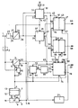
- the analog color video signal (FBAS signal), which is composed of a broadband brightness signal and a color carrier modulated with color signals, is fed to a terminal 1.
- FBAS signal which is composed of a broadband brightness signal and a color carrier modulated with color signals
- the two color difference signals (R-Y) and (B-Y) are simultaneously modulated onto a color carrier.
- the color difference signals are transmitted on alternating carriers in frequency modulation.
- These color video signals are fed to a first analog / digital converter 3 at a first input 4, possibly via a low-pass filter 2 which attenuates the color-bearer signals.
- the converter 3 receives a clock signal at a second input 5, which is a multiple, e.g. corresponds to 1135 times the line frequency of the signal fed to terminal 1.
- the clock signal for input 5 is supplied by output 6 of a clock stage 7.
- the line pulses are fed to its input 8 to a phase discriminator part 9.
- the clock frequency of 17.734375 MHz is generated in an oscillator part 10 and, divided by 1135, fed to the phase discriminator part 9 at the input 12. This provides a control signal which is fed to the oscillator 10 via a low-pass filter 11 for frequency control.
- the output oscillation of the oscillator 10 supplies the clock signal for the converter 3 to the output 6, possibly via a pulse shaper 13.
- the converter 3 with its 7-bit range can be optimally used for the image signal
- its amplitude range is alternately switched to the range of the image signals or to the range of the synchronous signals. This is done by means of a switchover signal, which is supplied by a switching stage 15, to which the color video signal is supplied at a first input 16 and the clock signal from the clock generator 7 at a second input 17.
- a changeover signal is formed in time with the line pulses, which corresponds to the interval in which the picture blanking signals or the synchronizing signals occur.
- the separated synchronizing pulses then occur, which are fed to further processing stages via an output 19 and of which the line pulses synchronize the clock oscillator 7 via the input 8.
- the digitized brightness signal is taken from an output 20 of stage 3 and is led to an output 22, preferably via a filter 21.
- the incoming signal from terminal 1 is passed on via a high pass 25, e.g. can be formed by a capacitor, a first input 26 of an analog-to-digital converter 27, which also comprises 7 bits and supplies the digitized color bit signal to an output 28.
- a clock signal is fed to the converter 27 from a second clock oscillator 30. This oscillates on a harmonic of the color carrier frequency, e.g. with a quartz 31, which may be switchable to a different frequency depending on the received standard and oscillates to about 17.73 MHz with PAL reception.
- the color synchronizing signal is fed to the oscillator 30 at an input 32 from the output 28 of the converter 29 and blanked with the aid of the synchronizing signals obtained from the output 18 of the converter 3, which are fed to an input 33 of the oscillator 30.
- the oscillator 30 is thereby synchronized to the frequency and the phase of the color synchronizing pulse. It delivers a clock signal at its output 34 which corresponds to four times the color carrier frequency and is fed to the clock input 29 of the converter 27 and further to a reference signal input 36 of a color demodulator 37 which receives the digital color signals at its input 38.
- the red and blue color difference signals (RY) and (BY) appear in digital form at the outputs 41 and 42 of the demodulator 37. These are fed to a first signal memory 43 or a second signal memory 44, each of which consists of a writing part 45 or 46. and a reading part 47 and 48 exist.
- the memories 43 and 44 are further supplied with clock signals from the oscillator 30 at inputs 51 and 52.
- the color signals supplied to the memories 43 and 44 at the inputs 53 and 54 are no longer modulated onto a carrier, but instead are video-frequency.
- the entrances 51 and 52 supplied clock signals thus only need to be at least twice the highest frequency of these color signals, for example 2.2 MHz corresponding to half the original color carrier frequency.
- the color signal values stored in this way are read out in the reading part 47 or 48 and transmitted at an output 55 or 56 under the control of address signals which are fed to an input 57 of the memory 43 or an input 58 of the memory 44 on the reading part 47 or 48.
- address signals are supplied by an address control stage 60.
- the clock signal used in the converter 3 for the brightness signal is fed to this stage 60 at an input 61.
- a signal is taken from the oscillator 30 at an output 62, which corresponds to a multiple of the color carrier frequency and at least approximately matches the clock signal at the input 5 of the converter 3 in the case of a color carrier frequency and line frequency in accordance with the standard.
- the signal from the output 62 is fed to an input 63 in the stage 60 and compared in a comparison stage 64 with the signal from the input 61.
- the difference determined in this way occurs at an output 65 of stage 64 and is fed to a computing stage 66.
- this stage e.g.
- the address transmitter 70 can be constructed in the form of a table, the setpoint of the sampling points of the converter 3 in the interval of the image signals of a line, e.g. 284, divided by the difference determined. Without taking fractions into account, a numerical value is then obtained which indicates after which number of sampling points of the brightness signal the number of sampling points of the color signals is one point more or less.
- This value is fed to the address transmitter 70 at a first input 71, a signal being fed to a second input 72 from an output 73 of the comparator 64, indicating the sign of the difference.
- the address transmitter 70 works with a clock fed to its input 74, which is taken from the output 6 of the oscillator 7.
- the address transmitter 60 supplies at its outputs 75 and 76 address control signals for the inputs 57 and 58 for the reading parts 47 and 48 of the memories 43 and 44.
- the signals supplied by the outputs 75 and 76 are such that the stored values in Cycles of a multiple of the line frequency are read out until, based on the same image interval, one clock has become more or one clock less effective when reading out than was effective during reading in the same time interval.
- the address control signal either samples a memory value twice or skips a memory value, so that the assigned value of the read interval is started again at the next read interval.
- a set signal is supplied to the inputs 79 and 80 of the read-write memory 43 and 44, respectively, with which the write part and, possibly a few key intervals later, the read part is reset to the initial state.
- the memories 43 and 44 need only be dimensioned for a number of signals which are approximately twice the color signal bandwidth, e.g. the color carrier frequency. Since the emitted signals are intended to interact with the brightness signal, which has a much higher sampling rate, which corresponds to approximately four times the color carrier frequency, each stored value can be sampled four times in succession when scanning in part 47 or 48 in order to obtain the same rate.
- the memories 43 and 44 only need to be dimensioned for the samples of half a line. If no frequency difference is found in stage 64, intermediate storage is not necessary, possibly only a delay by a few sampling intervals. On the other hand, when a difference of one point occurs, the read-write memories 43 and 44 make a correction after half a line. If the difference is larger, the correction is made after a corresponding fraction of a line. If the line is reset to the beginning after the correction, the line memory no longer needs to be.
Landscapes
- Engineering & Computer Science (AREA)
- Multimedia (AREA)
- Signal Processing (AREA)
- Processing Of Color Television Signals (AREA)
- Color Television Systems (AREA)
Claims (6)
Applications Claiming Priority (2)
| Application Number | Priority Date | Filing Date | Title |
|---|---|---|---|
| DE19823232316 DE3232316A1 (de) | 1982-08-31 | 1982-08-31 | Schaltungsanordnung zum umwandeln eines analogen farbvideosignals in ein digitales signal |
| DE3232316 | 1982-08-31 |
Publications (3)
| Publication Number | Publication Date |
|---|---|
| EP0104681A2 EP0104681A2 (fr) | 1984-04-04 |
| EP0104681A3 EP0104681A3 (en) | 1984-10-31 |
| EP0104681B1 true EP0104681B1 (fr) | 1987-06-10 |
Family
ID=6172120
Family Applications (1)
| Application Number | Title | Priority Date | Filing Date |
|---|---|---|---|
| EP83201223A Expired EP0104681B1 (fr) | 1982-08-31 | 1983-08-25 | Montage pour convertir un signal vidéo couleur analogique en un signal numérique |
Country Status (3)
| Country | Link |
|---|---|
| EP (1) | EP0104681B1 (fr) |
| JP (1) | JPS5961290A (fr) |
| DE (2) | DE3232316A1 (fr) |
Families Citing this family (5)
| Publication number | Priority date | Publication date | Assignee | Title |
|---|---|---|---|---|
| FR2565447B1 (fr) * | 1984-06-05 | 1987-08-21 | Software Based Systems Sbs | Dispositif de numerisation d'une image video et systeme de numerisation et de visualisation d'une image |
| DE3432314A1 (de) * | 1984-09-03 | 1986-03-13 | Philips Patentverwaltung Gmbh, 2000 Hamburg | Schaltungsanordnung zum ableiten digitaler farbsignale aus einem analogen fernsehsignal |
| US4635099A (en) * | 1985-02-04 | 1987-01-06 | Rca Corporation | Apparatus for detecting nonstandard video signals |
| GB2176669A (en) * | 1985-06-05 | 1986-12-31 | Philips Electronic Associated | Digitising television signals |
| DE3935330A1 (de) * | 1988-12-21 | 1991-04-25 | Thomson Brandt Gmbh | Verfahren zum abspeichern von farbfernsehsignalen |
-
1982
- 1982-08-31 DE DE19823232316 patent/DE3232316A1/de not_active Withdrawn
-
1983
- 1983-08-25 EP EP83201223A patent/EP0104681B1/fr not_active Expired
- 1983-08-25 DE DE8383201223T patent/DE3372052D1/de not_active Expired
- 1983-08-31 JP JP58158133A patent/JPS5961290A/ja active Pending
Also Published As
| Publication number | Publication date |
|---|---|
| EP0104681A2 (fr) | 1984-04-04 |
| JPS5961290A (ja) | 1984-04-07 |
| EP0104681A3 (en) | 1984-10-31 |
| DE3232316A1 (de) | 1984-03-01 |
| DE3372052D1 (en) | 1987-07-16 |
Similar Documents
| Publication | Publication Date | Title |
|---|---|---|
| DE2711947C3 (de) | Synchronisierschaltung für Videosignale | |
| DE3342335C2 (fr) | ||
| DE3305918C3 (de) | Schaltungsanordnung zum Verarbeiten eines trägermodulierten Analogsignals | |
| DE2520491B2 (de) | System und verfahren zum ausgleichen von zeitfehlern in videoartigen informationssignalen | |
| DE2735848A1 (de) | Anordnung zur bildung eines farbvideosignalgemisches und zum abspielen einer farbbildinformation von einem aufzeichnungstraeger | |
| DE2711948B2 (de) | Schaltungsanordnung zur Synchronisierung von Fernsehsignalen | |
| DE69121626T2 (de) | Einrichtung zur Fernsehsignalumwandlung | |
| DE3510213A1 (de) | Videosignalwiedergabegeraet | |
| EP0450445B1 (fr) | Circuit de traitement de signal de télévision numérique avec horloge de sortie orthogonale | |
| DE3435169A1 (de) | Digitales wandlersystem fuer farb-videosignale | |
| DE3637018C2 (de) | Adaptive Filteranordnung | |
| DE3737627C2 (de) | Fernsehgerät | |
| DE3603248C2 (fr) | ||
| DE3872117T2 (de) | Schaltung zur umwandlung eines impulses in eine kontinuierliche schwingung. | |
| DE3335677A1 (de) | Anordnung zur automatischen verstaerkungsregelung des farbartsignals in einem digitalen fernsehempfaenger | |
| EP0226649B1 (fr) | Circuit de réglage de chrominance d'un récepteur numérique de télévision | |
| DE69026007T2 (de) | Signalwellenformanzeigegerät | |
| DE3811115B4 (de) | Farbdemodulator zur Verwendung mit einem zeitfehlerkorrigierten Taktsignal | |
| EP0104681A2 (fr) | Montage pour convertir un signal vidéo couleur analogique en un signal numérique | |
| DE3829965C2 (fr) | ||
| DE4104773A1 (de) | Zeitdifferenz-korrekturschaltung fuer helligkeits- und chrominanzsignale | |
| DE69413608T2 (de) | Schaltung zur Verarbeitung eines Chrominanzsignals | |
| DE69227218T2 (de) | Bildsignalverarbeitungsvorrichtung | |
| DE69126505T2 (de) | Schaltung zum Aufzeichnen und Wiedergeben eines Referenzsignals für einen Zeitbasiskorrektor | |
| DE3856375T2 (de) | Fernsehempfänger mit verzerrungskorrigiertem Taktsignal |
Legal Events
| Date | Code | Title | Description |
|---|---|---|---|
| PUAI | Public reference made under article 153(3) epc to a published international application that has entered the european phase |
Free format text: ORIGINAL CODE: 0009012 |
|
| AK | Designated contracting states |
Designated state(s): DE FR GB |
|
| PUAL | Search report despatched |
Free format text: ORIGINAL CODE: 0009013 |
|
| AK | Designated contracting states |
Designated state(s): DE FR GB |
|
| 17P | Request for examination filed |
Effective date: 19841121 |
|
| 17Q | First examination report despatched |
Effective date: 19860203 |
|
| GRAA | (expected) grant |
Free format text: ORIGINAL CODE: 0009210 |
|
| AK | Designated contracting states |
Kind code of ref document: B1 Designated state(s): DE FR GB |
|
| REF | Corresponds to: |
Ref document number: 3372052 Country of ref document: DE Date of ref document: 19870716 |
|
| ET | Fr: translation filed | ||
| RAP2 | Party data changed (patent owner data changed or rights of a patent transferred) |
Owner name: N.V. PHILIPS' GLOEILAMPENFABRIEKEN Owner name: PHILIPS PATENTVERWALTUNG GMBH |
|
| PLBE | No opposition filed within time limit |
Free format text: ORIGINAL CODE: 0009261 |
|
| STAA | Information on the status of an ep patent application or granted ep patent |
Free format text: STATUS: NO OPPOSITION FILED WITHIN TIME LIMIT |
|
| 26N | No opposition filed | ||
| PGFP | Annual fee paid to national office [announced via postgrant information from national office to epo] |
Ref country code: DE Payment date: 19911028 Year of fee payment: 9 |
|
| PGFP | Annual fee paid to national office [announced via postgrant information from national office to epo] |
Ref country code: GB Payment date: 19920731 Year of fee payment: 10 |
|
| PGFP | Annual fee paid to national office [announced via postgrant information from national office to epo] |
Ref country code: FR Payment date: 19920819 Year of fee payment: 10 |
|
| PG25 | Lapsed in a contracting state [announced via postgrant information from national office to epo] |
Ref country code: DE Effective date: 19930501 |
|
| PG25 | Lapsed in a contracting state [announced via postgrant information from national office to epo] |
Ref country code: GB Effective date: 19930825 |
|
| GBPC | Gb: european patent ceased through non-payment of renewal fee |
Effective date: 19930825 |
|
| PG25 | Lapsed in a contracting state [announced via postgrant information from national office to epo] |
Ref country code: FR Effective date: 19940429 |
|
| REG | Reference to a national code |
Ref country code: FR Ref legal event code: ST |