EP0104708A2 - Photothermische Einrichtung - Google Patents
Photothermische Einrichtung Download PDFInfo
- Publication number
- EP0104708A2 EP0104708A2 EP83201363A EP83201363A EP0104708A2 EP 0104708 A2 EP0104708 A2 EP 0104708A2 EP 83201363 A EP83201363 A EP 83201363A EP 83201363 A EP83201363 A EP 83201363A EP 0104708 A2 EP0104708 A2 EP 0104708A2
- Authority
- EP
- European Patent Office
- Prior art keywords
- layer
- depositing
- further characterized
- amorphous
- boron
- Prior art date
- Legal status (The legal status is an assumption and is not a legal conclusion. Google has not performed a legal analysis and makes no representation as to the accuracy of the status listed.)
- Granted
Links
- 239000000463 material Substances 0.000 claims abstract description 125
- 230000005855 radiation Effects 0.000 claims abstract description 89
- ZOXJGFHDIHLPTG-UHFFFAOYSA-N Boron Chemical compound [B] ZOXJGFHDIHLPTG-UHFFFAOYSA-N 0.000 claims abstract description 71
- 229910052796 boron Inorganic materials 0.000 claims abstract description 71
- 229910000808 amorphous metal alloy Inorganic materials 0.000 claims abstract description 51
- 239000010703 silicon Substances 0.000 claims abstract description 48
- XUIMIQQOPSSXEZ-UHFFFAOYSA-N Silicon Chemical compound [Si] XUIMIQQOPSSXEZ-UHFFFAOYSA-N 0.000 claims abstract description 47
- 229910052710 silicon Inorganic materials 0.000 claims abstract description 41
- IJGRMHOSHXDMSA-UHFFFAOYSA-N Atomic nitrogen Chemical compound N#N IJGRMHOSHXDMSA-UHFFFAOYSA-N 0.000 claims abstract description 40
- ZOKXTWBITQBERF-UHFFFAOYSA-N Molybdenum Chemical compound [Mo] ZOKXTWBITQBERF-UHFFFAOYSA-N 0.000 claims abstract description 30
- 239000011733 molybdenum Substances 0.000 claims abstract description 30
- 229910052750 molybdenum Inorganic materials 0.000 claims abstract description 25
- GNPVGFCGXDBREM-UHFFFAOYSA-N germanium atom Chemical compound [Ge] GNPVGFCGXDBREM-UHFFFAOYSA-N 0.000 claims abstract description 21
- 229910052723 transition metal Inorganic materials 0.000 claims abstract description 17
- 150000003624 transition metals Chemical class 0.000 claims abstract description 17
- 229910052732 germanium Inorganic materials 0.000 claims abstract description 16
- 229910052757 nitrogen Inorganic materials 0.000 claims abstract description 12
- 239000010935 stainless steel Substances 0.000 claims abstract description 12
- 229910001220 stainless steel Inorganic materials 0.000 claims abstract description 12
- 238000004519 manufacturing process Methods 0.000 claims abstract description 6
- 238000000034 method Methods 0.000 claims abstract 24
- 238000000151 deposition Methods 0.000 claims description 59
- 239000006096 absorbing agent Substances 0.000 claims description 47
- 239000011358 absorbing material Substances 0.000 claims description 30
- 239000000758 substrate Substances 0.000 claims description 28
- 229910045601 alloy Inorganic materials 0.000 claims description 27
- 239000000956 alloy Substances 0.000 claims description 27
- QVGXLLKOCUKJST-UHFFFAOYSA-N atomic oxygen Chemical compound [O] QVGXLLKOCUKJST-UHFFFAOYSA-N 0.000 claims description 25
- 239000001301 oxygen Substances 0.000 claims description 25
- PXHVJJICTQNCMI-UHFFFAOYSA-N Nickel Chemical compound [Ni] PXHVJJICTQNCMI-UHFFFAOYSA-N 0.000 claims description 24
- 229910000979 O alloy Inorganic materials 0.000 claims description 17
- WFKWXMTUELFFGS-UHFFFAOYSA-N tungsten Chemical compound [W] WFKWXMTUELFFGS-UHFFFAOYSA-N 0.000 claims description 16
- 229910052721 tungsten Inorganic materials 0.000 claims description 16
- 239000010937 tungsten Substances 0.000 claims description 16
- 238000001228 spectrum Methods 0.000 claims description 14
- 229910001199 N alloy Inorganic materials 0.000 claims description 13
- 229910052759 nickel Inorganic materials 0.000 claims description 12
- 229910052760 oxygen Inorganic materials 0.000 claims description 11
- 150000001875 compounds Chemical class 0.000 claims description 10
- 230000008021 deposition Effects 0.000 claims description 9
- 150000003623 transition metal compounds Chemical class 0.000 claims description 8
- 229910000927 Ge alloy Inorganic materials 0.000 claims description 7
- 229910021417 amorphous silicon Inorganic materials 0.000 claims description 7
- HCHKCACWOHOZIP-UHFFFAOYSA-N Zinc Chemical compound [Zn] HCHKCACWOHOZIP-UHFFFAOYSA-N 0.000 claims description 5
- OBNDGIHQAIXEAO-UHFFFAOYSA-N [O].[Si] Chemical compound [O].[Si] OBNDGIHQAIXEAO-UHFFFAOYSA-N 0.000 claims description 5
- 229910052725 zinc Inorganic materials 0.000 claims description 5
- 239000011701 zinc Substances 0.000 claims description 5
- 229910000521 B alloy Inorganic materials 0.000 claims description 4
- BASFCYQUMIYNBI-UHFFFAOYSA-N platinum Chemical compound [Pt] BASFCYQUMIYNBI-UHFFFAOYSA-N 0.000 claims description 4
- RTAQQCXQSZGOHL-UHFFFAOYSA-N Titanium Chemical compound [Ti] RTAQQCXQSZGOHL-UHFFFAOYSA-N 0.000 claims description 3
- QCWXUUIWCKQGHC-UHFFFAOYSA-N Zirconium Chemical compound [Zr] QCWXUUIWCKQGHC-UHFFFAOYSA-N 0.000 claims description 3
- 229910052735 hafnium Inorganic materials 0.000 claims description 3
- VBJZVLUMGGDVMO-UHFFFAOYSA-N hafnium atom Chemical compound [Hf] VBJZVLUMGGDVMO-UHFFFAOYSA-N 0.000 claims description 3
- 150000004820 halides Chemical class 0.000 claims description 3
- 239000010936 titanium Substances 0.000 claims description 3
- 229910052719 titanium Inorganic materials 0.000 claims description 3
- 229910052726 zirconium Inorganic materials 0.000 claims description 3
- UFHFLCQGNIYNRP-UHFFFAOYSA-N Hydrogen Chemical compound [H][H] UFHFLCQGNIYNRP-UHFFFAOYSA-N 0.000 claims description 2
- TZHYBRCGYCPGBQ-UHFFFAOYSA-N [B].[N] Chemical compound [B].[N] TZHYBRCGYCPGBQ-UHFFFAOYSA-N 0.000 claims description 2
- UMVBXBACMIOFDO-UHFFFAOYSA-N [N].[Si] Chemical compound [N].[Si] UMVBXBACMIOFDO-UHFFFAOYSA-N 0.000 claims description 2
- 239000001257 hydrogen Substances 0.000 claims description 2
- 229910052739 hydrogen Inorganic materials 0.000 claims description 2
- 229910052697 platinum Inorganic materials 0.000 claims description 2
- 238000010438 heat treatment Methods 0.000 claims 4
- 229910000687 transition metal group alloy Inorganic materials 0.000 claims 2
- OKTJSMMVPCPJKN-UHFFFAOYSA-N Carbon Chemical compound [C] OKTJSMMVPCPJKN-UHFFFAOYSA-N 0.000 claims 1
- 229910052799 carbon Inorganic materials 0.000 claims 1
- 229910000676 Si alloy Inorganic materials 0.000 abstract description 12
- 230000031700 light absorption Effects 0.000 abstract description 7
- 238000010521 absorption reaction Methods 0.000 description 47
- 239000000203 mixture Substances 0.000 description 17
- 238000002310 reflectometry Methods 0.000 description 16
- OAKJQQAXSVQMHS-UHFFFAOYSA-N Hydrazine Chemical compound NN OAKJQQAXSVQMHS-UHFFFAOYSA-N 0.000 description 12
- 229910052782 aluminium Inorganic materials 0.000 description 11
- XAGFODPZIPBFFR-UHFFFAOYSA-N aluminium Chemical compound [Al] XAGFODPZIPBFFR-UHFFFAOYSA-N 0.000 description 11
- 229910001182 Mo alloy Inorganic materials 0.000 description 8
- 230000008901 benefit Effects 0.000 description 8
- 239000002178 crystalline material Substances 0.000 description 6
- 239000007789 gas Substances 0.000 description 6
- 150000004678 hydrides Chemical class 0.000 description 6
- 239000010408 film Substances 0.000 description 5
- 239000011521 glass Substances 0.000 description 5
- 229910052751 metal Inorganic materials 0.000 description 5
- 239000002184 metal Substances 0.000 description 5
- VTYDSHHBXXPBBQ-UHFFFAOYSA-N boron germanium Chemical compound [B].[Ge] VTYDSHHBXXPBBQ-UHFFFAOYSA-N 0.000 description 4
- 238000006243 chemical reaction Methods 0.000 description 4
- 230000003247 decreasing effect Effects 0.000 description 4
- 150000004767 nitrides Chemical class 0.000 description 4
- VYZAMTAEIAYCRO-UHFFFAOYSA-N Chromium Chemical compound [Cr] VYZAMTAEIAYCRO-UHFFFAOYSA-N 0.000 description 3
- RYGMFSIKBFXOCR-UHFFFAOYSA-N Copper Chemical compound [Cu] RYGMFSIKBFXOCR-UHFFFAOYSA-N 0.000 description 3
- BLRPTPMANUNPDV-UHFFFAOYSA-N Silane Chemical compound [SiH4] BLRPTPMANUNPDV-UHFFFAOYSA-N 0.000 description 3
- CFOAUMXQOCBWNJ-UHFFFAOYSA-N [B].[Si] Chemical compound [B].[Si] CFOAUMXQOCBWNJ-UHFFFAOYSA-N 0.000 description 3
- LGLOITKZTDVGOE-UHFFFAOYSA-N boranylidynemolybdenum Chemical compound [Mo]#B LGLOITKZTDVGOE-UHFFFAOYSA-N 0.000 description 3
- 238000005229 chemical vapour deposition Methods 0.000 description 3
- 239000010949 copper Substances 0.000 description 3
- 229910000431 copper oxide Inorganic materials 0.000 description 3
- VNWKTOKETHGBQD-UHFFFAOYSA-N methane Chemical compound C VNWKTOKETHGBQD-UHFFFAOYSA-N 0.000 description 3
- 239000011541 reaction mixture Substances 0.000 description 3
- XLYOFNOQVPJJNP-UHFFFAOYSA-N water Substances O XLYOFNOQVPJJNP-UHFFFAOYSA-N 0.000 description 3
- QPLDLSVMHZLSFG-UHFFFAOYSA-N Copper oxide Chemical compound [Cu]=O QPLDLSVMHZLSFG-UHFFFAOYSA-N 0.000 description 2
- 239000005751 Copper oxide Substances 0.000 description 2
- 229910017333 Mo(CO)6 Inorganic materials 0.000 description 2
- BQCADISMDOOEFD-UHFFFAOYSA-N Silver Chemical compound [Ag] BQCADISMDOOEFD-UHFFFAOYSA-N 0.000 description 2
- HSFWRNGVRCDJHI-UHFFFAOYSA-N alpha-acetylene Natural products C#C HSFWRNGVRCDJHI-UHFFFAOYSA-N 0.000 description 2
- 235000013405 beer Nutrition 0.000 description 2
- 239000011248 coating agent Substances 0.000 description 2
- 238000000576 coating method Methods 0.000 description 2
- 229910017052 cobalt Inorganic materials 0.000 description 2
- 239000010941 cobalt Substances 0.000 description 2
- GUTLYIVDDKVIGB-UHFFFAOYSA-N cobalt atom Chemical compound [Co] GUTLYIVDDKVIGB-UHFFFAOYSA-N 0.000 description 2
- 229910052802 copper Inorganic materials 0.000 description 2
- 230000008713 feedback mechanism Effects 0.000 description 2
- PCHJSUWPFVWCPO-UHFFFAOYSA-N gold Chemical compound [Au] PCHJSUWPFVWCPO-UHFFFAOYSA-N 0.000 description 2
- 229910052737 gold Inorganic materials 0.000 description 2
- 239000010931 gold Substances 0.000 description 2
- 150000001247 metal acetylides Chemical class 0.000 description 2
- 150000002739 metals Chemical class 0.000 description 2
- 229910000480 nickel oxide Inorganic materials 0.000 description 2
- 230000003647 oxidation Effects 0.000 description 2
- 238000007254 oxidation reaction Methods 0.000 description 2
- GNRSAWUEBMWBQH-UHFFFAOYSA-N oxonickel Chemical compound [Ni]=O GNRSAWUEBMWBQH-UHFFFAOYSA-N 0.000 description 2
- 230000037361 pathway Effects 0.000 description 2
- 229910000077 silane Inorganic materials 0.000 description 2
- 229910052709 silver Inorganic materials 0.000 description 2
- 239000004332 silver Substances 0.000 description 2
- RZVAJINKPMORJF-UHFFFAOYSA-N Acetaminophen Chemical compound CC(=O)NC1=CC=C(O)C=C1 RZVAJINKPMORJF-UHFFFAOYSA-N 0.000 description 1
- 239000004215 Carbon black (E152) Substances 0.000 description 1
- KRHYYFGTRYWZRS-UHFFFAOYSA-M Fluoride anion Chemical compound [F-] KRHYYFGTRYWZRS-UHFFFAOYSA-M 0.000 description 1
- WGLPBDUCMAPZCE-UHFFFAOYSA-N Trioxochromium Chemical compound O=[Cr](=O)=O WGLPBDUCMAPZCE-UHFFFAOYSA-N 0.000 description 1
- UBMXAAKAFOKSPA-UHFFFAOYSA-N [N].[O].[Si] Chemical compound [N].[O].[Si] UBMXAAKAFOKSPA-UHFFFAOYSA-N 0.000 description 1
- 238000007743 anodising Methods 0.000 description 1
- 125000002915 carbonyl group Chemical group [*:2]C([*:1])=O 0.000 description 1
- 230000015556 catabolic process Effects 0.000 description 1
- 230000008859 change Effects 0.000 description 1
- 239000007795 chemical reaction product Substances 0.000 description 1
- 229910052804 chromium Inorganic materials 0.000 description 1
- 239000011651 chromium Substances 0.000 description 1
- 229910000423 chromium oxide Inorganic materials 0.000 description 1
- 239000002131 composite material Substances 0.000 description 1
- 239000012141 concentrate Substances 0.000 description 1
- 238000007739 conversion coating Methods 0.000 description 1
- 230000007812 deficiency Effects 0.000 description 1
- 238000006731 degradation reaction Methods 0.000 description 1
- 125000002534 ethynyl group Chemical group [H]C#C* 0.000 description 1
- 230000001747 exhibiting effect Effects 0.000 description 1
- -1 fluoride compound Chemical class 0.000 description 1
- QUZPNFFHZPRKJD-UHFFFAOYSA-N germane Chemical compound [GeH4] QUZPNFFHZPRKJD-UHFFFAOYSA-N 0.000 description 1
- 229910052986 germanium hydride Inorganic materials 0.000 description 1
- 229930195733 hydrocarbon Natural products 0.000 description 1
- 150000002430 hydrocarbons Chemical class 0.000 description 1
- 230000006872 improvement Effects 0.000 description 1
- 239000007788 liquid Substances 0.000 description 1
- 238000005297 material degradation process Methods 0.000 description 1
- 229910001507 metal halide Inorganic materials 0.000 description 1
- 150000005309 metal halides Chemical class 0.000 description 1
- 230000004048 modification Effects 0.000 description 1
- 238000012986 modification Methods 0.000 description 1
- QJGQUHMNIGDVPM-UHFFFAOYSA-N nitrogen group Chemical group [N] QJGQUHMNIGDVPM-UHFFFAOYSA-N 0.000 description 1
- 238000010943 off-gassing Methods 0.000 description 1
- 239000003973 paint Substances 0.000 description 1
- 239000002245 particle Substances 0.000 description 1
- 239000005297 pyrex Substances 0.000 description 1
- 239000010453 quartz Substances 0.000 description 1
- 239000000376 reactant Substances 0.000 description 1
- 238000009877 rendering Methods 0.000 description 1
- VYPSYNLAJGMNEJ-UHFFFAOYSA-N silicon dioxide Inorganic materials O=[Si]=O VYPSYNLAJGMNEJ-UHFFFAOYSA-N 0.000 description 1
- 239000007787 solid Substances 0.000 description 1
- 239000000126 substance Substances 0.000 description 1
- 239000010409 thin film Substances 0.000 description 1
- 239000011573 trace mineral Substances 0.000 description 1
- 235000013619 trace mineral Nutrition 0.000 description 1
- 238000001429 visible spectrum Methods 0.000 description 1
Images


Classifications
-
- F—MECHANICAL ENGINEERING; LIGHTING; HEATING; WEAPONS; BLASTING
- F24—HEATING; RANGES; VENTILATING
- F24S—SOLAR HEAT COLLECTORS; SOLAR HEAT SYSTEMS
- F24S70/00—Details of absorbing elements
- F24S70/30—Auxiliary coatings, e.g. anti-reflective coatings
-
- F—MECHANICAL ENGINEERING; LIGHTING; HEATING; WEAPONS; BLASTING
- F24—HEATING; RANGES; VENTILATING
- F24S—SOLAR HEAT COLLECTORS; SOLAR HEAT SYSTEMS
- F24S70/00—Details of absorbing elements
- F24S70/20—Details of absorbing elements characterised by absorbing coatings; characterised by surface treatment for increasing absorption
- F24S70/225—Details of absorbing elements characterised by absorbing coatings; characterised by surface treatment for increasing absorption for spectrally selective absorption
-
- F—MECHANICAL ENGINEERING; LIGHTING; HEATING; WEAPONS; BLASTING
- F24—HEATING; RANGES; VENTILATING
- F24S—SOLAR HEAT COLLECTORS; SOLAR HEAT SYSTEMS
- F24S70/00—Details of absorbing elements
- F24S70/20—Details of absorbing elements characterised by absorbing coatings; characterised by surface treatment for increasing absorption
- F24S70/25—Coatings made of metallic material
-
- Y—GENERAL TAGGING OF NEW TECHNOLOGICAL DEVELOPMENTS; GENERAL TAGGING OF CROSS-SECTIONAL TECHNOLOGIES SPANNING OVER SEVERAL SECTIONS OF THE IPC; TECHNICAL SUBJECTS COVERED BY FORMER USPC CROSS-REFERENCE ART COLLECTIONS [XRACs] AND DIGESTS
- Y02—TECHNOLOGIES OR APPLICATIONS FOR MITIGATION OR ADAPTATION AGAINST CLIMATE CHANGE
- Y02E—REDUCTION OF GREENHOUSE GAS [GHG] EMISSIONS, RELATED TO ENERGY GENERATION, TRANSMISSION OR DISTRIBUTION
- Y02E10/00—Energy generation through renewable energy sources
- Y02E10/40—Solar thermal energy, e.g. solar towers
-
- Y—GENERAL TAGGING OF NEW TECHNOLOGICAL DEVELOPMENTS; GENERAL TAGGING OF CROSS-SECTIONAL TECHNOLOGIES SPANNING OVER SEVERAL SECTIONS OF THE IPC; TECHNICAL SUBJECTS COVERED BY FORMER USPC CROSS-REFERENCE ART COLLECTIONS [XRACs] AND DIGESTS
- Y02—TECHNOLOGIES OR APPLICATIONS FOR MITIGATION OR ADAPTATION AGAINST CLIMATE CHANGE
- Y02P—CLIMATE CHANGE MITIGATION TECHNOLOGIES IN THE PRODUCTION OR PROCESSING OF GOODS
- Y02P20/00—Technologies relating to chemical industry
- Y02P20/10—Process efficiency
- Y02P20/133—Renewable energy sources, e.g. sunlight
-
- Y—GENERAL TAGGING OF NEW TECHNOLOGICAL DEVELOPMENTS; GENERAL TAGGING OF CROSS-SECTIONAL TECHNOLOGIES SPANNING OVER SEVERAL SECTIONS OF THE IPC; TECHNICAL SUBJECTS COVERED BY FORMER USPC CROSS-REFERENCE ART COLLECTIONS [XRACs] AND DIGESTS
- Y10—TECHNICAL SUBJECTS COVERED BY FORMER USPC
- Y10S—TECHNICAL SUBJECTS COVERED BY FORMER USPC CROSS-REFERENCE ART COLLECTIONS [XRACs] AND DIGESTS
- Y10S126/00—Stoves and furnaces
- Y10S126/907—Absorber coating
- Y10S126/908—Particular chemical
-
- Y—GENERAL TAGGING OF NEW TECHNOLOGICAL DEVELOPMENTS; GENERAL TAGGING OF CROSS-SECTIONAL TECHNOLOGIES SPANNING OVER SEVERAL SECTIONS OF THE IPC; TECHNICAL SUBJECTS COVERED BY FORMER USPC CROSS-REFERENCE ART COLLECTIONS [XRACs] AND DIGESTS
- Y10—TECHNICAL SUBJECTS COVERED BY FORMER USPC
- Y10T—TECHNICAL SUBJECTS COVERED BY FORMER US CLASSIFICATION
- Y10T428/00—Stock material or miscellaneous articles
- Y10T428/12—All metal or with adjacent metals
- Y10T428/12493—Composite; i.e., plural, adjacent, spatially distinct metal components [e.g., layers, joint, etc.]
- Y10T428/12535—Composite; i.e., plural, adjacent, spatially distinct metal components [e.g., layers, joint, etc.] with additional, spatially distinct nonmetal component
- Y10T428/12542—More than one such component
- Y10T428/12549—Adjacent to each other
-
- Y—GENERAL TAGGING OF NEW TECHNOLOGICAL DEVELOPMENTS; GENERAL TAGGING OF CROSS-SECTIONAL TECHNOLOGIES SPANNING OVER SEVERAL SECTIONS OF THE IPC; TECHNICAL SUBJECTS COVERED BY FORMER USPC CROSS-REFERENCE ART COLLECTIONS [XRACs] AND DIGESTS
- Y10—TECHNICAL SUBJECTS COVERED BY FORMER USPC
- Y10T—TECHNICAL SUBJECTS COVERED BY FORMER US CLASSIFICATION
- Y10T428/00—Stock material or miscellaneous articles
- Y10T428/12—All metal or with adjacent metals
- Y10T428/12493—Composite; i.e., plural, adjacent, spatially distinct metal components [e.g., layers, joint, etc.]
- Y10T428/12535—Composite; i.e., plural, adjacent, spatially distinct metal components [e.g., layers, joint, etc.] with additional, spatially distinct nonmetal component
- Y10T428/12576—Boride, carbide or nitride component
-
- Y—GENERAL TAGGING OF NEW TECHNOLOGICAL DEVELOPMENTS; GENERAL TAGGING OF CROSS-SECTIONAL TECHNOLOGIES SPANNING OVER SEVERAL SECTIONS OF THE IPC; TECHNICAL SUBJECTS COVERED BY FORMER USPC CROSS-REFERENCE ART COLLECTIONS [XRACs] AND DIGESTS
- Y10—TECHNICAL SUBJECTS COVERED BY FORMER USPC
- Y10T—TECHNICAL SUBJECTS COVERED BY FORMER US CLASSIFICATION
- Y10T428/00—Stock material or miscellaneous articles
- Y10T428/12—All metal or with adjacent metals
- Y10T428/12493—Composite; i.e., plural, adjacent, spatially distinct metal components [e.g., layers, joint, etc.]
- Y10T428/12535—Composite; i.e., plural, adjacent, spatially distinct metal components [e.g., layers, joint, etc.] with additional, spatially distinct nonmetal component
- Y10T428/12597—Noncrystalline silica or noncrystalline plural-oxide component [e.g., glass, etc.]
Definitions
- This invention relates to new and improved materials and devices for improved selective absorption of light energy for use in photothermal applications.
- Such devices are generally in the nature.of a layered composite of materials which, as a whole, absorb sunlight and convert it to heat.
- a selective absorber for photothermal applications should exhibit high absorption (ie., low reflectivity) in the terrestrial solar spectrum (TSS), wavelengths of from about 350 nm to about 2300 nm. This is desirable because the terrestrial solar spectrum comprises about 98% of the solar power which typically reaches the surface of the earth and is therefore generally most usable for generating heat.
- the device should also exhibit low emissivity (i.e.
- TIR thermal infra-red
- compositions and devices are currently in use as absorbers of solar energy.
- materials like black paint. These materials are solar-nonselective. While exhibiting acceptable absorption in the TSS, these materials exhibit low reflectivity in the TIR. Hence, these materials are inefficient selective absorbers because the low reflectivity in the TIR results in high emissivity in the TIR. Such a characteristic, as noted above, results in emission of power as heat and thus makes these substances far less desirable for photothermal applications.
- Another type of prior art material used in solar absorbers is aluminum with a nickel anodized coating.
- the aluminum provides reflectance in the infra-red regions which is desirable.
- the nickel anodizing coats the aluminum resulting in a black colored oxide over the aluminum which provides absorption and the rough texture provides some antireflection.
- the biggest problem with this approach is that an aluminum substrate must be used. Hence, other forms of substrates cannot be used without first applying a layer of aluminum thereto. This, of course, adds extra steps and therefore extra time and expense to the manufacturing process.
- black chrome A third type of prior art material is referred to as black chrome.
- This type of material is generally composed of nickel electrolyzed in a chrome bath. The surface is coated with chromium and chromium oxide particles which provide both antireflection and absorption. This approach suffers from the same deficiency as the nickel anodized aluminum selective absorbers in that they cannot be applied to a non-conductive substrate without the interposition of a conductive layer.
- black cobalt C 03 0 4
- C 03 0 4 Another prior art material in use as a selective absorber of light energy is black cobalt, C 03 0 4 . This is produced by electrolyzing a substrate in a cobalt bath.
- a conductive layer is required if a non-conductive substrate is to be employed.
- the materials are copper oxide deposited on copper and nickel oxide deposited on nickel conversion coatings.
- the copper oxide exhibits satisfactory absorption and low emissivity.
- the nickel coating has a texture which provides antireflection and the nickel oxide provides absorption.
- collectors In evacuated tube-type systems, oxidation is not a problem. However, a further source of inefficiency becomes apparent when a selective absorber made in solution is used in conjunction with these types of collectors.
- These collectors are generally constructed of two glass tubes, one having a smaller diameter than and being longitudinally arranged within the other. The space between the tubes is evacuated to prevent heat transfer to the outside.
- the selective absorber material covers the outer surface of the inner tube. In such a configuration, light will penetrate the outer tube and be absorbed by the selective absorber while, theoretically, emission of the heat absorbed is blocked by the evacuated space.
- the problem arises from the fact that materials made in solution contain water. Materials made in solution out gas water and other gasses into the space between the tubes. The outgassing causes the loss of the vacuum which in turn allows loss through heat transfer.
- the device of the present invention utilizes a selective absorber layer of an amorphous material which provides a number of advantages over the prior art materials.
- the absorption edge of an amorphous material can be changed at will.
- the material can be adjusted for maximum absorption over the TSS and minimum emissivity of the TIR wavelengths.
- amorphous materials of the present invention can be produced which exhibit greater absorption of radiant energy than crystalline materials having the same composition.
- index of refraction of an amorphous material can be graded more uniformly from one extreme to the other than can crystalline materials. This is desirable because a gradual increase, as a function of film depth, in the index of refraction causes light to be more readily absorbed. Abrupt changes in the index of refraction contribute to greatly increased reflectivity and therefore decreased absorption.
- Amorphous materials can be produced with controlled and predetermined indices of refraction not possible with crystalline and polycrystalline materials of the same composition. This allows matching of the indices of refraction of two adjoining materials to decrease the reflection off the interface of the materials and therefore increase absorption.
- amorphous films lack polycrystalline grain boundaries. This is desirable because such grain boundaries act as oxygen-or moisture pathways. Oxygen and moisture are two of the predominate causes of film degradation.
- amorphous materials are easier and less expensive to deposit and can be deposited at temperatures lower than those required for depositing crystalline or polycrystalline materials. Lower deposition temperatures lead to substantially decreased damage to surfaces on which the material is deposited which in turn allows a substantially greater number of possible substrates to be utilized with the device.
- the present invention provides new and improved materials and devices for improved selective absorption of light energy for use in photothermal applications and a method of manufacturing same.
- the new photothermal device includes a layer of solar radiation absorbing material which exhibits high absorption in the terrestrial solar spectrum (TSS) (i.e. wavelengths of from about 350 nm to about 2300 nm).
- TSS terrestrial solar spectrum
- thermal infrared radiation reflecting material which exhibits low emissivity in the thermal infrared (TIR) portion of the spectrum (i.e. wavelengths above 2300 nm).
- a solar antireflecting layer is included to minimize reflectivity in the TSS.
- the thermal infrared radiation reflecting material preferably comprises a transition metal or stainless steel.
- Aluminum or coinage metals namely copper, silver or gold, can also be used, especially in conjunction with thick absorber layers.
- the selective absorber layer comprises amorphous boron or an amorphous boron alloy including silicon, germanium, or molybdenum deposited over the infrared reflecting layer.
- amorphous materials as a selective absorber of radiant energy provides a number of significant advantages over the prior art materials including greatly increased absorption of radiant energy . over crystalline materials having the same composition and an absorption edge which can be adjusted at will to maximize absorption over the TSS and minimize emissivity over the TIR.
- the solar antireflecting layer preferably comprises an amorphous alloy of either nitrogen or oxygen and either silicon or boron which is deposited over the solar absorbing layer and serves to decrease surface reflectance and therefore aid absorption of light energy.
- a first object of the invention is to provide a material for use in photothermal applications, the material characterized by containing amorphous boron.
- a second object of the invention is to provide a photothermal device for converting solar radiation to heat, the device characterized by a layer of thermal infrared radiation reflecting material, a layer of solar radiation absorbing material overlying the layer of reflecting material, and a layer of solar radiation antireflecting material overlying the layer of absorbing material, the layer of solar radiation absorbing material including amorphous boron.
- a third object of the invention is to provide a method of making a selective absorber for converting solar radiation to heat characterized by providing a layer of thermal- infrared radiation reflecting material, depositing a layer of solar radiation absorbing material over the thermal infrared radiation reflecting material, the solar radiation absorbing material including amorphous boron, and depositing a layer of solar radiation antireflecting material over the layer of solar absorbing material.
- a fourth object of the invention is to provide an apparatus for making a selective absorber for converting solar energy to heat characterized by means for providing a layer of thermal infrared radiation reflecting material, means for depositing a layer of solar radiation absorbing material over the thermal infrared radiation reflecting material, the solar radiation absorbing material including amorphous boron, and means for depositing a layer of solar radiation antireflecting material over the layer of solar absorbing material.
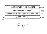
- FIG. 1 there is shown a partial, cross-sectional side view of an improved device 10 for the selective absorption of light energy according to the present invention.
- the device includes a substrate 12, a thermal infrared radiation reflecting layer 14, a solar absorption layer 16 and a solar radiation antireflecting layer 18.
- the thermal infrared radiation reflecting layer 14 comprises a transition metal or stainless steel or an alloy or compound of a transition metal or stainless steel. These materials are employed because they exhibit low emissivity (i.e. high reflectivity) in the thermal infrared (TIR) portion of the spectrum, generally above 2300 nm and medium to high solar radiation absorption. The low emissivity in the TIR is highly desirable because these are the wavelengths at which bodies tend to radiate heat.
- Transition metal compounds which work particularly well as thermal infrared radiation reflect-.
- ing materials are borides, carbides and nitrides of zirconium, hafnium, titanium, molybdenum and tungsten.
- the thermal infrared radiation reflecting layer 14 can also serve as the device substrate or the infrared reflecting layer 14 can be deposited on a separate substrate 12 of, for example, glass or stainless steel.
- thermal infrared reflecting layer 14 when the thermal infrared reflecting layer 14 also serves as the device substrate 12, aluminum or the coinage metals, namely copper, silver or gold, can be used to form the substrate and the infrared reflecting layer 14. These materials are particularly efficacious when employed in conjunction with thick selective absorber layers 16.
- thick absorber layers applicants refer to those absorber layers 16 of the order of 1 micron or greater in thickness.
- alloys of the aforementioned compounds also may be utilized with satisfactory results.
- a preferred embodiment of the solar absorbing layer 16 comprises preferably amorphous boron or amorphous alloys of boron and silicon, germanium or molybdenum.
- the boron-silicon alloy preferably contains from about 5 percent to about 85 percent silicon.
- the boron-germanium alloy preferably contains up to about 95 percent germanium.
- the boron-molybdenum alloy contains up to 20 percent molybdenum.
- amorphous boron materials exhibit excellent absorption in the TSS as illustrated hereinafter with respect to Figs 3-5. Moreover, the amorphous structure of the material provides a number of significant advantages over the prior art materials.
- the absorption edge of an amorphous material can be changed at will.
- the material can be adjusted for maximum absorption over the TSS and minimum emissivity of the TIR wavelengths as illustrated hereinafter with respect to Figs. 9-17.
- amorphous ra- terials of the present invention can be produced which exhibit greater absorption of radiant energy than crystalline materials having the same composition.
- the solar radiation antireflecting material layer 18 preferably comprises an amorphous alloy of either boron and nitrogen, silicon and nitrogen, silicon and oxygen or silicon, oxygen and ri- trogen.
- amorphous alloy of either boron and nitrogen, silicon and nitrogen, silicon and oxygen or silicon, oxygen and ri- trogen.
- Amorphous materials such as these can also be produced with controlled and predetermined indices of refraction as illustrated hereinafter with respect to Figs. 6-8. Such control and predetermination are not possible with crystalline and polycrystalline materials of the same composition. This allows matching of the indices of refraction of two adjoining materials to decrease the reflection off the interface of the materials and therefore increase absorption.
- amorphous materials lack polycrystalline grain boundaries. This is particularly desirable because such grain boundaries act as conduction pathways for oxygen and moisture. Oxygen and moisture are two of the predominate causes of material degradation.
- the index of refraction of the solar radiation antireflecting material will be tailored to equal approximately 85 to 100% of the square root of the index refraction of the solar absorption material. This, as noted above, will substantially eliminate any reflection of incoming light off the interface of the materials and therefore increase absorption.
- a schematic representation of one preferred embodiment of a system 20 for manufacturing the devices of the present invention comprises cylinders 22 for holding reaction gases, a flow controller 24, a bubbler 26, a sublimator 28, assorted shutoff valves 30a through 30e, a primary manifold 32 and a secondary manifold 34.
- the system 20 further comprises a bypass line 38, a reactor tube 40, a cylindrical furnace 42, couplers 44, a temperature control 46, a feedback mechanism 48, a coarse pressure adjustment valve 50, a pressure reader 52, a pressure control 54, a fine pressure adjustment valve 56 and a pump 58.
- the reaction gases are held in cylinders 22 and routed through flow controllers 24 and shutoff valves 30a to the primary manifold 32 where the majority of the reaction mixtures are combined.
- the bubbler 26 functions to vaporize liquid hydrazine (N 2 H 4 ) which is used to deposit nitrides of transition metals when they are incorporated into the infrared radiation reflecting layer 14. Hydrazine is also used to deposit the nitrogenous alloys of silicon, silicon and oxygen or boron to be used in the antireflecting layer 18.
- the sublimator 28 is used to convert solid molybdenum hexacarbonyl (Mo(CO) 6 ) to a gas. This material is used in the deposition of the amorphous alloy of boron and molybdenum when incorporated into the solar absorption layer 16.
- the secondary manifold 34 serves to mix the gaseous hydrazine or molybdenum hexacarbonyl when the bubbler 26 or sublimator 28 are used, with the reaction mixture formed in the primary manifold 32.
- valves 30a are closed and valves 30b and 30c are opened.
- valves 30b and 30c are closed and valves 30a opened.
- shutoff valve 30d is inserted in the system 20.
- the by--pass line 38 and its shutoff valve 30e are interposed between the secondary manifold 34 and shutoff valve 30d. Initially valve 30d will be closed and valves 30e will be opened so that the bypass line 38 can be used to bypass the reactor tube 40 and check the mixture before actual deposition. This is accomplished by reading the partial pressure of the reactants at the pressure reader 52.
- shutoff valves 30e are closed and shutoff valve 30d in front of coupler 44 is opened to allow the reaction mixture to enter the reactor tube 40.
- the reactor tube is a Pyrex or quartz chemical vapor deposition hot wall reactor 40 surrounded by a cylindrical furnace 42 used to heat the substrate 12 to a given reaction temperature (discussed infra).
- the furnace 42 is connected to a temperature control 46 with a suitable feedback mechanism 48 from inside the reactor tube 40.
- the ambient pressure within the reactor tube 40 during deposition is monitored by the pressure reader 52 which in turn is connected to a pressure control 54.
- the pressure control 54 is used in conjunction with the pump 58, coarse pressure adjustment valve 50 and the fine pressure adjustment valve 56 to control the ambient pressure within the reactor tube 40 when deposition is taking place.
- an infrared reflecting layer 14 comprises a transition metal or stainless steel.
- the transition metals which have been found particularly useful in the present context are tungsten, molybdenum, zinc, platinum and nickel. Deposition of any of these can be accomplished by pyrolyzing a carbonyl or halide of the particular metal or reacting the halide of the particular metal with hydrogen.
- compounds of transition metals can be employed in the TIR layer 14.
- the borides, carbides and nitrides of zirconium, hafnium, titanium, molybdenum and tungsten can be used. These compounds may be deposited using the system 20 by reacting the metal halide with BC1 3 or B 2 H 6 in the case of the boride, a hydrocarbon such as methane (CH 4 ) or acetylene (C 2 H 2 ) in the case of the carbide, or a hydride of nitrogen such as NH 3 or N 2 H 4 in the case of the nitride. All of these reactions, whether to deposit the metal or the compound, would be carried out, according to the preferred embodiment, at elevated substrate temperatures, preferably in the range of about 800°C to about 1200°C.
- tungsten is used in the TIR layer and is deposited over a glass substrate.
- tungsten is often reacted for deposition purposes in the form of its fluoride compound (i.e. WF 6 ) and fluoride reaction products will etch glass
- an intervening layer of an amorphous silicon alloy is first deposited over the glass. This layer need only be approximately 300 nm thick.
- the silicon alloy is deposited by chemical vapor deposition utilizing silane in a hot wall reactor at a substrate temperature of about 600°C and a pressure in the range of 0.27 to 4.0 kPa.
- the solar absorber material layer 16 is next deposited over the thermal infrared radiation reflecting layer 14.
- amorphous boron is employed as the solar absorber and it is deposited using the hydride, B 2 H 6 , at substrate temperatures in the range of about 250°C to about 477°C and pressure generally below 6.67 kPa.
- Another embodiment calls for the use of an amorphous alloy of boron and germanium which is deposited with a similar use of the corresponding hydrides, B 2 H 6 and GeH 4 , at substrate temperatures in the range of about 377°C to about 477°C and pressure generally below 1.33 kPa.
- an amorphous alloy of boron and molybdenum can be used as the solar absorber 16.
- the hydride of boron, B 2 H 6 is reacted with molybdenum hexacarbonyl, Mo(CO)6, at substrate temperatures in the range of about 250°C to about 300°C and pressure generally below 267 kPa
- the solar radiation antireflecting material layer 18 is deposited over the solar absorber 16.
- the antireflecting layer 18 to comprise an amorphous alloy of either boron and nitrogen, silicon and nitrogen, silicon and oxygen or silicon, oxygen and nitrogen.
- the boron-nitrogen alloy is preferably deposited by reacting the hydride of boron, B 2 H 6 , with N 2 H 4 at substrate temperatures generally in excess of 350°C and pressure at or below atmospheric pressure.
- the silicon-nitrogen alloy is preferably deposited by reacting silane, SiH 4 , with a hydride of nitrogen (e.g. N 2 H 4 ) at substrate temperatures generaly in excess of 500°C and preferably in the approximate range of about 650°C to about 700°C.
- a hydride of nitrogen e.g. N 2 H 4
- substrate temperatures generaly in excess of 500°C and preferably in the approximate range of about 650°C to about 700°C.
- oxygen or water vapor to the appropriate deposition atmosphere.
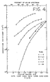
- Figs. 3 to 5 there are shown the absorption characteristics for three of the specific materials discussed above as preferred embodiments of the solar absorber layer 16.
- Fig. 3 represents the coefficient of absorption of the amorphous boron-silicon alloy for five given percent compositions of silicon and boron at a given wavelength and corresponding photon energy of light being absorbed. It should be noted that the photon energy and the wavelength are inversely proportional by a factor of 1.237. In other words: where X is the wavelength in microns and PE is the photon energy in eV.
- Fig. 4 represents a similar graph of the absorption characteristics for a solar absorber layer 16 comprising an amorphous alloy of boron and molybdenum. Note that the designation "nil” for the amount of molybdenum in the boron-molybdenum alloy sample which resulted in that particular curve in Fig. 4 represents a composition containing trace elements of molybdenum.
- Fig. 5 illustrates the same information for an absorber layer 16 comprising an amorphous alloy of boron and germanium.
- each material has a characteristic absorption coefficient for a given photon energy or wavelength of light depending on the percent composition of the material.
- the incident light after being transmitted through the selective absorber layer 16, is reflected off the thermal infrared reflecting layer 14 and back through the absorber layer 16. Therefore, assuming 100% reflectivity in the thermal infrared reflecting layer 14, the absorber layer 16 has an effective thickness twice that of its actual thickness. That is to say that Beer's Law, with respect to the present invention, can be written as:
- all of the solar absorber materials absorb energy of shorter wavelength and higher photon energy more readily than light of longer wavelength and lower photon energy.
- Figs. 6, 7 and 8 there is shown in each a graph of index of refraction versus percent composition of solar absorber material for three representative photon energies or light wavelengths.
- Fig. 6 represents the aforementioned parameters for an embodiment of the solar absorber layer 16 comprising an amorphous alloy of boron and silicon.
- Fig. 7 refers to the amorphous boron-molybdenum alloy and
- Fig. 8 is the same plot for the amorphous boron-germanium alloy.
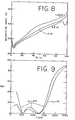
- Figs. 9 through 17 are graphs of percent reflectance versus wavelength for various representative device configurations. It should be remembered that reflectance is inversely proportional to absorption and therefore these graphs illustrate the efficiency of absorption in the TSS as well as reflectivity (or emissivity) in the TIR for the particular device configuration tested.
- Figs. 9-17 graph percent reflectance for wavelengths up to 2500 nm, it should be noted that the infrared portion of the spectrum extends as high as wavelengths of approximately 100,000 nm. Also, for a given operating temperature, a body will tend to emit energy (e.g. photons) centered around a particular wavelength. In other words, emittance, a parameter to be minimized, will be fixed by the temperature at which the device is operated. Depending on the specific application in which the device of the present invention is to be used, the operating temperature could be between approximately 100°C and approximately 500°C.' The wavelength around which a body will emit the maximum energy for a given operating temperature is given by the equation:
- a body at an operating temperature of about 130°C, a body will emit its maximum energy at wavelengths centered around 7000 nm.
- materials are employed in the thermal infrared reflecting layer that have as one of their properties extremely high reflectivity in the infrared portion of the spectrum.
- many applications of the present invention will include an operating temperature around 130°C.
- such an operating temperature will induce emission of the maximum amount of photons at wavelengths centered around 7000 nm.
- molybdenum exhibits 98.3% reflectivity, tungsten 97%, stainless steel 90% and nickel 92%.
- the thermal infrared reflectivity of the device will be within 1% less than the reflectivity of the bare infrared reflector material at any wavelength of interest.
- Figs. 9-17 graph only up to wavelengths of 2500 nm because this is all that is required to establish the absorption characteristics of the device of the present invention in the visible spectrum. Above 2500 nm, the reflectivity is easily calculated as discussed above.
- Fig. 9 compares theoretical and empirical results.
- the upper solid line represents the theoretical percent reflectance over a spectrum from approximately 300 to approximately 2500 nm of a device having a tungsten TIR layer 14, a solar absorber layer 16 comprising an amorphous alloy of 60% boron and 40% germanium, and an antireflecting layer 18 comprising an amorphous alloy of silicon and oxygen.
- the lower line represents actual experimental results for a device having a tungsten TIR layer 14, an amorphous boron-germanium solar absorber layer 16 containing 50% germanium and an antireflecting layer comprising an amorphous silicon-oxygen alloy.
- Fig. 10 shows these same parameters for a similar device but utilizing stainless steel as a TIR layer 14. Similar results were achieved but for a reflectance approaching 70% at 2500 nm. This is still a marked improvement over prior art devices.
- the device for which results are plotted in Fig. 12 utilizes a solar antireflecting layer of an amorphous alloy of silicon and oxygen and a solar absorbing layer comprising an amorphous alloy of approximately 30% boron and 70% germanium.
- the thermal infrared reflecting layer comprises nickel. This configuration exhibited absorption in the TSS of approximately 85% with reflectance at 2500 nm approaching 70%.
- Fig. 13 plots the percent reflectance for a device similar to that employed with respect to Fig. 12 but having an infrared reflecting layer comprising zinc.
- the percent absorption in the TSS, 84.3% is very similar to that obtained with the same device but having a nickel infrared reflecting layer.
- the change to a zinc infrared reflecting layer we see an increase in the percent reflectance to approximately 85%.
- Fig. 14 the results are plotted for a device similar to that tested for the data in Fig. 12 but having an infrared reflecting layer comprising molybdenum.
- the antireflecting layer and absorber layer comprise amorphous alloys of silicon-oxygen and boron-germanium respectively.
- the device exhibited 88% absorption in the TSS and reflectance at 2500 nm exceeding 70%.
- Fig. 15 is a graph of the same parameters as Figs. 9-14 but for a device having a TIR layer 14 comprising aluminum, a solar absorbing layer 16 comprising an amorphous alloy of boron and silicon, and an antireflecting layer 18 comprising 50% amorphous boron and 50% nitrogen.
- the inventors have achieved absorption in the TSS of approximately 94% while maintaining a still very respectable reflectance figure at 2500 nm.
- Figs. 16 and 17 plot the results for two devices, each of which having antireflecting layers comprising amorphous silicon-oxygen alloys and absorber layers comprising amorphous boron-silicon alloys in proportion of 65% boron and 35% silicon.
- the device of Fig. 16 has an infrared reflecting layer of tungsten. It absorbed 89% of the light in the TSS while reflecting 50% of the light at 2500 nm.
- the device of Fig. 17 had an infrared reflecting layer comprising molybdenum. It absorbed 86.8% of the light in the TSS and the reflectance increased to better than 60%.
Landscapes
- Engineering & Computer Science (AREA)
- Physics & Mathematics (AREA)
- Combustion & Propulsion (AREA)
- Mechanical Engineering (AREA)
- Sustainable Development (AREA)
- Sustainable Energy (AREA)
- Thermal Sciences (AREA)
- Chemical & Material Sciences (AREA)
- General Engineering & Computer Science (AREA)
- Life Sciences & Earth Sciences (AREA)
- Spectroscopy & Molecular Physics (AREA)
- Photovoltaic Devices (AREA)
- Laminated Bodies (AREA)
- Other Surface Treatments For Metallic Materials (AREA)
- Optical Filters (AREA)
- Heating, Cooling, Or Curing Plastics Or The Like In General (AREA)
Priority Applications (1)
| Application Number | Priority Date | Filing Date | Title |
|---|---|---|---|
| AT83201363T ATE28508T1 (de) | 1982-09-24 | 1983-09-23 | Photothermische einrichtung. |
Applications Claiming Priority (2)
| Application Number | Priority Date | Filing Date | Title |
|---|---|---|---|
| US06/423,425 US4582764A (en) | 1982-09-24 | 1982-09-24 | Selective absorber amorphous alloys and devices |
| US423425 | 1982-09-24 |
Publications (3)
| Publication Number | Publication Date |
|---|---|
| EP0104708A2 true EP0104708A2 (de) | 1984-04-04 |
| EP0104708A3 EP0104708A3 (en) | 1985-01-23 |
| EP0104708B1 EP0104708B1 (de) | 1987-07-22 |
Family
ID=23678869
Family Applications (1)
| Application Number | Title | Priority Date | Filing Date |
|---|---|---|---|
| EP83201363A Expired EP0104708B1 (de) | 1982-09-24 | 1983-09-23 | Photothermische Einrichtung |
Country Status (6)
| Country | Link |
|---|---|
| US (1) | US4582764A (de) |
| EP (1) | EP0104708B1 (de) |
| JP (1) | JPS5980747A (de) |
| AT (1) | ATE28508T1 (de) |
| CA (1) | CA1242367A (de) |
| DE (1) | DE3372660D1 (de) |
Cited By (5)
| Publication number | Priority date | Publication date | Assignee | Title |
|---|---|---|---|---|
| BE1007236A3 (fr) * | 1993-07-07 | 1995-05-02 | Vadder Paul De | Collecteur solaire du type thermique. |
| WO1996002798A1 (de) * | 1994-07-15 | 1996-02-01 | Thomas Eisenhammer | Strahlungswandler zur umsetzung von elektromagnetischer strahlung in wärme und von wärme in elektromagnetische strahlung |
| EP1217315A1 (de) * | 2000-12-20 | 2002-06-26 | ALANOD Aluminium-Veredlung GmbH & Co. KG | Solarkollektorelement |
| ES2316321A1 (es) * | 2008-10-20 | 2009-04-01 | Abengoa Solar New Technologies, S.A. | Recubrimiento absorbente selectivo solar y metodo de fabricacion. |
| ITMI20121572A1 (it) * | 2012-09-21 | 2014-03-22 | Eni Spa | Procedimento per la produzione di un rivestimento otticamente selettivo di un substrato per dispositivi ricevitori solari ad alta temperatura e relativo materiale ottenuto |
Families Citing this family (45)
| Publication number | Priority date | Publication date | Assignee | Title |
|---|---|---|---|---|
| US4702955A (en) * | 1985-07-24 | 1987-10-27 | Ovonic Synthetic Materials Company, Inc. | Multilayer decorative coating |
| US4775203A (en) * | 1987-02-13 | 1988-10-04 | General Electric Company | Optical scattering free metal oxide films and methods of making the same |
| US5035949A (en) * | 1988-12-05 | 1991-07-30 | Martin Marietta Corporation | High-temperature, high-emissivity, optically black boron surface |
| US5004308A (en) * | 1990-05-23 | 1991-04-02 | Rockwell International Corporation | Rugate reflector |
| US6223743B1 (en) * | 1999-05-18 | 2001-05-01 | Melvin L. Prueitt | Solar power generation and energy storage system |
| US6650478B1 (en) | 1999-08-20 | 2003-11-18 | Cpfilms Inc. | Optical filter for a window |
| US20040126594A1 (en) * | 2002-06-06 | 2004-07-01 | Carlo Rubbia | Surface coating for a collector tube of a linear parabolic solar concentrator |
| DE102004010689B3 (de) * | 2004-02-27 | 2005-06-30 | Schott Ag | Absorber mit einer strahlungsselektiven Absorberbeschichtung und Verfahren zu seiner Herstellung |
| DE102004038233A1 (de) * | 2004-08-05 | 2006-03-16 | Schott Ag | Solarabsorber |
| US7372610B2 (en) | 2005-02-23 | 2008-05-13 | Sage Electrochromics, Inc. | Electrochromic devices and methods |
| SE530464C2 (sv) * | 2005-08-02 | 2008-06-17 | Sunstrip Ab | Nickel-aluminiumoxid-belagd solabsorbator |
| DE102005063130B4 (de) * | 2005-12-30 | 2017-07-27 | Advanced Micro Devices, Inc. | Verfahren zum Bilden einer Grabenisolationsstruktur mit unterschiedlicher Verspannung |
| US9147778B2 (en) * | 2006-11-07 | 2015-09-29 | First Solar, Inc. | Photovoltaic devices including nitrogen-containing metal contact |
| TW200934889A (en) * | 2007-10-12 | 2009-08-16 | Nihon Parkerizing | Light-absorbing member and method of manufacturing same |
| AU2007360138B2 (en) * | 2007-10-18 | 2013-09-19 | Midwest Research Institue | High temperature solar selective coatings |
| US20090199847A1 (en) * | 2008-02-11 | 2009-08-13 | James Hawley | Earth based solar collector |
| DE102009022059A1 (de) * | 2009-05-20 | 2010-11-25 | Schott Solar Ag | Strahlungsselektive Absorberbeschichtung und Absorberrohr mit strahlungsselektiver Absorberbeschichtung |
| DE202009015334U1 (de) * | 2009-11-11 | 2010-02-25 | Almeco-Tinox Gmbh | Optisch wirksames Mehrschichtsystem für solare Absorption |
| US20170031525A1 (en) | 2010-05-14 | 2017-02-02 | Racing Optics, Inc. | Touch screen shield |
| US20120234313A1 (en) * | 2011-03-18 | 2012-09-20 | ZYRUS Beteiligungsgesellschaft mbH & Co., Patente I KG | Solar collector and method for manufacturing such a solar collector |
| CN102261757B (zh) * | 2011-07-06 | 2013-03-06 | 张浙军 | 带氮化硅介质选择吸收涂层的太阳能集热器芯及制备方法 |
| JP5896889B2 (ja) * | 2012-12-07 | 2016-03-30 | 株式会社豊田自動織機 | 光学選択膜 |
| WO2014204671A1 (en) * | 2013-06-20 | 2014-12-24 | University Of Houston System | GRADIENT SiNO ANTI-REFLECTIVE LAYERS IN SOLAR SELECTIVE COATINGS |
| US9482448B2 (en) | 2013-09-04 | 2016-11-01 | Taiwan Ziolar Technology Co. Ltd. | Solar thermal collector, solar thermal heater and method of manufacturing the same |
| CN104976802A (zh) * | 2014-04-11 | 2015-10-14 | 太浩科技有限公司 | 一种太阳光谱选择性吸收涂层及其制备方法 |
| CN104976803A (zh) * | 2014-04-11 | 2015-10-14 | 太浩科技有限公司 | 一种太阳光谱选择性吸收涂层及其制备方法 |
| US9295297B2 (en) | 2014-06-17 | 2016-03-29 | Racing Optics, Inc. | Adhesive mountable stack of removable layers |
| WO2016205672A1 (en) * | 2015-06-19 | 2016-12-22 | University Of Houston System | Selective solar absorbers with tuned oxygen deficiency and methods of fabrication thereof |
| JP6197833B2 (ja) * | 2015-06-30 | 2017-09-20 | 株式会社豊田自動織機 | 太陽熱集熱管及び太陽熱発電装置 |
| CN106152576B (zh) * | 2016-09-14 | 2018-05-25 | 兰州交通大学 | 基于难熔金属硼化物的高温光谱选择性吸收涂层及制备方法 |
| MX2020010413A (es) | 2018-04-04 | 2021-06-18 | The Research Foundation Of The State Univ Of New York | Sistemas y metodos de refrigeracion pasiva y radiador para la misma. |
| WO2020160492A1 (en) | 2019-02-01 | 2020-08-06 | Racing Optics, Inc. | Thermoform windshield stack with integrated formable mold |
| US11846788B2 (en) | 2019-02-01 | 2023-12-19 | Racing Optics, Inc. | Thermoform windshield stack with integrated formable mold |
| US11364715B2 (en) | 2019-05-21 | 2022-06-21 | Racing Optics, Inc. | Polymer safety glazing for vehicles |
| US11648723B2 (en) | 2019-12-03 | 2023-05-16 | Racing Optics, Inc. | Method and apparatus for reducing non-normal incidence distortion in glazing films |
| US11912001B2 (en) | 2019-12-03 | 2024-02-27 | Ro Technologies, Llc | Method and apparatus for reducing non-normal incidence distortion in glazing films |
| US11548356B2 (en) | 2020-03-10 | 2023-01-10 | Racing Optics, Inc. | Protective barrier for safety glazing |
| US20210285661A1 (en) | 2020-03-10 | 2021-09-16 | Wolf Steel Ltd. | Heating and cooling appliance |
| US11490667B1 (en) | 2021-06-08 | 2022-11-08 | Racing Optics, Inc. | Low haze UV blocking removable lens stack |
| US12140781B2 (en) | 2021-07-27 | 2024-11-12 | Laminated Film Llc | Low reflectance removable lens stack |
| US11709296B2 (en) | 2021-07-27 | 2023-07-25 | Racing Optics, Inc. | Low reflectance removable lens stack |
| US11307329B1 (en) | 2021-07-27 | 2022-04-19 | Racing Optics, Inc. | Low reflectance removable lens stack |
| US12162330B2 (en) | 2022-02-08 | 2024-12-10 | Ro Technologies, Llc | Multi-layer windshield film having progressive thickness layers |
| US11933943B2 (en) | 2022-06-06 | 2024-03-19 | Laminated Film Llc | Stack of sterile peelable lenses with low creep |
| US11808952B1 (en) | 2022-09-26 | 2023-11-07 | Racing Optics, Inc. | Low static optical removable lens stack |
Family Cites Families (12)
| Publication number | Priority date | Publication date | Assignee | Title |
|---|---|---|---|---|
| US4098956A (en) * | 1976-08-11 | 1978-07-04 | The United States Of America As Represented By The Secretary Of The Interior | Spectrally selective solar absorbers |
| US4126150A (en) * | 1977-03-28 | 1978-11-21 | Rca Corporation | Photovoltaic device having increased absorption efficiency |
| US4177474A (en) * | 1977-05-18 | 1979-12-04 | Energy Conversion Devices, Inc. | High temperature amorphous semiconductor member and method of making the same |
| US4149025A (en) * | 1977-11-16 | 1979-04-10 | Vasile Niculescu | Method of fabricating thermoelectric power generator modules |
| US4226897A (en) * | 1977-12-05 | 1980-10-07 | Plasma Physics Corporation | Method of forming semiconducting materials and barriers |
| US4166880A (en) * | 1978-01-18 | 1979-09-04 | Solamat Incorporated | Solar energy device |
| US4286009A (en) * | 1978-02-16 | 1981-08-25 | Corning Glass Works | Composite solar absorber coatings |
| US4264358A (en) * | 1979-02-12 | 1981-04-28 | California Institute Of Technology | Semiconducting glasses with flux pinning inclusions |
| US4431708A (en) * | 1979-12-19 | 1984-02-14 | The United States Of America As Represented By The United States Department Of Energy | Annealed CVD molybdenum thin film surface |
| US4334523A (en) * | 1980-06-23 | 1982-06-15 | Owens-Illinois, Inc. | Solar energy collector having solar selective coating of low reflectance |
| US4356815A (en) * | 1980-08-19 | 1982-11-02 | Owens-Illinois, Inc. | Solar energy collector having an absorber element of coated foil |
| US4416916A (en) * | 1982-03-04 | 1983-11-22 | Engelhard Corporation | Thin film solar energy collector |
-
1982
- 1982-09-24 US US06/423,425 patent/US4582764A/en not_active Expired - Fee Related
-
1983
- 1983-09-22 JP JP58176100A patent/JPS5980747A/ja active Pending
- 1983-09-23 CA CA000437433A patent/CA1242367A/en not_active Expired
- 1983-09-23 DE DE8383201363T patent/DE3372660D1/de not_active Expired
- 1983-09-23 AT AT83201363T patent/ATE28508T1/de not_active IP Right Cessation
- 1983-09-23 EP EP83201363A patent/EP0104708B1/de not_active Expired
Cited By (13)
| Publication number | Priority date | Publication date | Assignee | Title |
|---|---|---|---|---|
| BE1007236A3 (fr) * | 1993-07-07 | 1995-05-02 | Vadder Paul De | Collecteur solaire du type thermique. |
| WO1996002798A1 (de) * | 1994-07-15 | 1996-02-01 | Thomas Eisenhammer | Strahlungswandler zur umsetzung von elektromagnetischer strahlung in wärme und von wärme in elektromagnetische strahlung |
| EP1217315A1 (de) * | 2000-12-20 | 2002-06-26 | ALANOD Aluminium-Veredlung GmbH & Co. KG | Solarkollektorelement |
| CN102203024A (zh) * | 2008-10-20 | 2011-09-28 | 阿文戈亚太阳能新技术公司 | 选择性太阳能吸收涂层及其制备方法 |
| WO2010046509A1 (es) * | 2008-10-20 | 2010-04-29 | Abengoa Solar New Technologies, S.A. | Recubrimiento absorbente selectivo solar y método de fabricación |
| ES2316321B2 (es) * | 2008-10-20 | 2010-12-14 | Abengoa Solar New Technologies, S.A. | Recubrimiento absorbente selectivo solar y metodo de fabricacion. |
| ES2316321A1 (es) * | 2008-10-20 | 2009-04-01 | Abengoa Solar New Technologies, S.A. | Recubrimiento absorbente selectivo solar y metodo de fabricacion. |
| US9423157B2 (en) | 2008-10-20 | 2016-08-23 | Abengoa Solar New Technologies, S.A. | Selective solar absorbent coating and manufacturing method |
| US10126020B2 (en) | 2008-10-20 | 2018-11-13 | Abengoa Solar New Technologies, S.A. | Selective solar absorbing coating and manufacturing method |
| ITMI20121572A1 (it) * | 2012-09-21 | 2014-03-22 | Eni Spa | Procedimento per la produzione di un rivestimento otticamente selettivo di un substrato per dispositivi ricevitori solari ad alta temperatura e relativo materiale ottenuto |
| WO2014044712A1 (en) * | 2012-09-21 | 2014-03-27 | Eni S.P.A. | Process for the production of an optically selective coating of a substrate for high temperature receiver solar devices and relative material obtained |
| US9786799B2 (en) | 2012-09-21 | 2017-10-10 | Eni S.P.A. | Process for the production of an optically selective coating of a substrate for high temperature receiver solar devices and relative material obtained |
| AU2013320297B2 (en) * | 2012-09-21 | 2018-02-22 | Eni S.P.A. | Process for the production of an optically selective coating of a substrate for high temperature receiver solar devices and relative material obtained |
Also Published As
| Publication number | Publication date |
|---|---|
| DE3372660D1 (en) | 1987-08-27 |
| JPS5980747A (ja) | 1984-05-10 |
| US4582764A (en) | 1986-04-15 |
| EP0104708A3 (en) | 1985-01-23 |
| EP0104708B1 (de) | 1987-07-22 |
| ATE28508T1 (de) | 1987-08-15 |
| CA1242367A (en) | 1988-09-27 |
Similar Documents
| Publication | Publication Date | Title |
|---|---|---|
| US4582764A (en) | Selective absorber amorphous alloys and devices | |
| EP0107412B1 (de) | Solarselektive Oberflächenbeschichtung | |
| US4334523A (en) | Solar energy collector having solar selective coating of low reflectance | |
| US4431708A (en) | Annealed CVD molybdenum thin film surface | |
| Seraphin | Spectrally selective surfaces and their impact on photothermal solar energy conversion | |
| JP6566041B2 (ja) | 熱光変換部材 | |
| US4584428A (en) | Solar energy converter employing a fluorescent wavelength shifter | |
| Seraphin | Chemical vapor deposition of spectrally selective surfaces for high temperature photothermal conversion | |
| JP6521176B2 (ja) | 熱光変換部材 | |
| Chain et al. | Highly reflecting molybdenum thin films having significant solar absorptance | |
| EP4189304B1 (de) | Spektral selektive solarabsorberbeschichtung | |
| Chain et al. | Chemically vapor-deposited black molybdenum films of high IR reflectance and significant solar absorptance | |
| US4710254A (en) | Process for fabricating a solar energy converter employing a fluorescent wavelength shifter | |
| Gurev et al. | High temperature; stable, spectrally selective solar absorbers for thermochemical hydrogen production | |
| Masterson | Selective surfaces for solar-thermal conversion | |
| Melamed et al. | Survey of selective absorber coatings for solar energy technology | |
| Spitz | Selective surfaces for high temperature solar photothermal conversion | |
| Allred et al. | Spectrally selective surfaces by chemical vapor deposition | |
| Carver et al. | CVD molybdenum films of high infrared reflectance and significant solar absorptance | |
| EP3835682B1 (de) | Solarwärmesammelrohr | |
| Gesheva et al. | Black tungsten selective optical coatings for photothermal solar energy conversion | |
| Seraphin | Thin films in photothermal solar energy conversion | |
| Martin et al. | Sputtered Si: H alloys for edge filters: application to thermophotovoltaics | |
| Mattox et al. | A survey of selective solar absorbers and their limitations | |
| Jacobson | Chemical vapor deposition: applying the technology to optics |
Legal Events
| Date | Code | Title | Description |
|---|---|---|---|
| PUAI | Public reference made under article 153(3) epc to a published international application that has entered the european phase |
Free format text: ORIGINAL CODE: 0009012 |
|
| AK | Designated contracting states |
Designated state(s): AT BE CH DE FR GB IT LI LU NL SE |
|
| PUAL | Search report despatched |
Free format text: ORIGINAL CODE: 0009013 |
|
| AK | Designated contracting states |
Designated state(s): AT BE CH DE FR GB IT LI LU NL SE |
|
| 17P | Request for examination filed |
Effective date: 19850722 |
|
| 17Q | First examination report despatched |
Effective date: 19860324 |
|
| GRAA | (expected) grant |
Free format text: ORIGINAL CODE: 0009210 |
|
| AK | Designated contracting states |
Kind code of ref document: B1 Designated state(s): AT BE CH DE FR GB IT LI LU NL SE |
|
| REF | Corresponds to: |
Ref document number: 28508 Country of ref document: AT Date of ref document: 19870815 Kind code of ref document: T |
|
| ITF | It: translation for a ep patent filed | ||
| REF | Corresponds to: |
Ref document number: 3372660 Country of ref document: DE Date of ref document: 19870827 |
|
| PG25 | Lapsed in a contracting state [announced via postgrant information from national office to epo] |
Ref country code: LU Free format text: LAPSE BECAUSE OF NON-PAYMENT OF DUE FEES Effective date: 19870930 |
|
| PGFP | Annual fee paid to national office [announced via postgrant information from national office to epo] |
Ref country code: NL Payment date: 19870930 Year of fee payment: 5 |
|
| ET | Fr: translation filed | ||
| PLBE | No opposition filed within time limit |
Free format text: ORIGINAL CODE: 0009261 |
|
| STAA | Information on the status of an ep patent application or granted ep patent |
Free format text: STATUS: NO OPPOSITION FILED WITHIN TIME LIMIT |
|
| 26N | No opposition filed | ||
| PG25 | Lapsed in a contracting state [announced via postgrant information from national office to epo] |
Ref country code: GB Effective date: 19880923 Ref country code: AT Effective date: 19880923 |
|
| PG25 | Lapsed in a contracting state [announced via postgrant information from national office to epo] |
Ref country code: SE Effective date: 19880924 |
|
| PG25 | Lapsed in a contracting state [announced via postgrant information from national office to epo] |
Ref country code: LI Effective date: 19880930 Ref country code: CH Effective date: 19880930 Ref country code: BE Effective date: 19880930 |
|
| BERE | Be: lapsed |
Owner name: ENERGY CONVERSION DEVICES INC. Effective date: 19880930 |
|
| PG25 | Lapsed in a contracting state [announced via postgrant information from national office to epo] |
Ref country code: NL Effective date: 19890401 |
|
| NLV4 | Nl: lapsed or anulled due to non-payment of the annual fee | ||
| PG25 | Lapsed in a contracting state [announced via postgrant information from national office to epo] |
Ref country code: FR Free format text: LAPSE BECAUSE OF NON-PAYMENT OF DUE FEES Effective date: 19890531 |
|
| REG | Reference to a national code |
Ref country code: CH Ref legal event code: PL |
|
| GBPC | Gb: european patent ceased through non-payment of renewal fee | ||
| PG25 | Lapsed in a contracting state [announced via postgrant information from national office to epo] |
Ref country code: DE Effective date: 19890601 |
|
| REG | Reference to a national code |
Ref country code: FR Ref legal event code: ST |
|
| PGFP | Annual fee paid to national office [announced via postgrant information from national office to epo] |
Ref country code: SE Payment date: 19890906 Year of fee payment: 7 |
|
| ITTA | It: last paid annual fee | ||
| EUG | Se: european patent has lapsed |
Ref document number: 83201363.5 Effective date: 19890712 |