EP0105214A2 - Méthode et dispositif pour écrire des motifs lithographique de grandes dimensions - Google Patents
Méthode et dispositif pour écrire des motifs lithographique de grandes dimensions Download PDFInfo
- Publication number
- EP0105214A2 EP0105214A2 EP83108762A EP83108762A EP0105214A2 EP 0105214 A2 EP0105214 A2 EP 0105214A2 EP 83108762 A EP83108762 A EP 83108762A EP 83108762 A EP83108762 A EP 83108762A EP 0105214 A2 EP0105214 A2 EP 0105214A2
- Authority
- EP
- European Patent Office
- Prior art keywords
- workpiece
- pattern
- successive
- writing
- written
- Prior art date
- Legal status (The legal status is an assumption and is not a legal conclusion. Google has not performed a legal analysis and makes no representation as to the accuracy of the status listed.)
- Granted
Links
Images


Classifications
-
- H—ELECTRICITY
- H01—ELECTRIC ELEMENTS
- H01J—ELECTRIC DISCHARGE TUBES OR DISCHARGE LAMPS
- H01J37/00—Discharge tubes with provision for introducing objects or material to be exposed to the discharge, e.g. for the purpose of examination or processing thereof
- H01J37/30—Electron-beam or ion-beam tubes for localised treatment of objects
- H01J37/317—Electron-beam or ion-beam tubes for localised treatment of objects for changing properties of the objects or for applying thin layers thereon, e.g. for ion implantation
- H01J37/3174—Particle-beam lithography, e.g. electron beam lithography
-
- B—PERFORMING OPERATIONS; TRANSPORTING
- B82—NANOTECHNOLOGY
- B82Y—SPECIFIC USES OR APPLICATIONS OF NANOSTRUCTURES; MEASUREMENT OR ANALYSIS OF NANOSTRUCTURES; MANUFACTURE OR TREATMENT OF NANOSTRUCTURES
- B82Y10/00—Nanotechnology for information processing, storage or transmission, e.g. quantum computing or single electron logic
-
- B—PERFORMING OPERATIONS; TRANSPORTING
- B82—NANOTECHNOLOGY
- B82Y—SPECIFIC USES OR APPLICATIONS OF NANOSTRUCTURES; MEASUREMENT OR ANALYSIS OF NANOSTRUCTURES; MANUFACTURE OR TREATMENT OF NANOSTRUCTURES
- B82Y40/00—Manufacture or treatment of nanostructures
-
- H—ELECTRICITY
- H01—ELECTRIC ELEMENTS
- H01J—ELECTRIC DISCHARGE TUBES OR DISCHARGE LAMPS
- H01J37/00—Discharge tubes with provision for introducing objects or material to be exposed to the discharge, e.g. for the purpose of examination or processing thereof
- H01J37/30—Electron-beam or ion-beam tubes for localised treatment of objects
- H01J37/302—Controlling tubes by external information, e.g. program control
- H01J37/3023—Program control
- H01J37/3026—Patterning strategy
-
- H—ELECTRICITY
- H01—ELECTRIC ELEMENTS
- H01J—ELECTRIC DISCHARGE TUBES OR DISCHARGE LAMPS
- H01J2237/00—Discharge tubes exposing object to beam, e.g. for analysis treatment, etching, imaging
- H01J2237/15—Means for deflecting or directing discharge
-
- H—ELECTRICITY
- H01—ELECTRIC ELEMENTS
- H01J—ELECTRIC DISCHARGE TUBES OR DISCHARGE LAMPS
- H01J2237/00—Discharge tubes exposing object to beam, e.g. for analysis treatment, etching, imaging
- H01J2237/20—Positioning, supporting, modifying or maintaining the physical state of objects being observed or treated
- H01J2237/202—Movement
- H01J2237/20278—Motorised movement
- H01J2237/20285—Motorised movement computer-controlled
-
- H—ELECTRICITY
- H01—ELECTRIC ELEMENTS
- H01J—ELECTRIC DISCHARGE TUBES OR DISCHARGE LAMPS
- H01J2237/00—Discharge tubes exposing object to beam, e.g. for analysis treatment, etching, imaging
- H01J2237/30—Electron or ion beam tubes for processing objects
- H01J2237/304—Controlling tubes
- H01J2237/30455—Correction during exposure
-
- H—ELECTRICITY
- H01—ELECTRIC ELEMENTS
- H01J—ELECTRIC DISCHARGE TUBES OR DISCHARGE LAMPS
- H01J2237/00—Discharge tubes exposing object to beam, e.g. for analysis treatment, etching, imaging
- H01J2237/30—Electron or ion beam tubes for processing objects
- H01J2237/304—Controlling tubes
- H01J2237/30472—Controlling the beam
- H01J2237/30483—Scanning
- H01J2237/30494—Vector scan
-
- H—ELECTRICITY
- H01—ELECTRIC ELEMENTS
- H01J—ELECTRIC DISCHARGE TUBES OR DISCHARGE LAMPS
- H01J2237/00—Discharge tubes exposing object to beam, e.g. for analysis treatment, etching, imaging
- H01J2237/30—Electron or ion beam tubes for processing objects
- H01J2237/317—Processing objects on a microscale
- H01J2237/3175—Lithography
- H01J2237/31761—Patterning strategy
- H01J2237/31764—Dividing into sub-patterns
-
- H—ELECTRICITY
- H01—ELECTRIC ELEMENTS
- H01J—ELECTRIC DISCHARGE TUBES OR DISCHARGE LAMPS
- H01J2237/00—Discharge tubes exposing object to beam, e.g. for analysis treatment, etching, imaging
- H01J2237/30—Electron or ion beam tubes for processing objects
- H01J2237/317—Processing objects on a microscale
- H01J2237/3175—Lithography
- H01J2237/31776—Shaped beam
Definitions
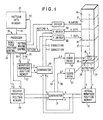
- the present invention provides apparatus for writing a pattern having a size larger than the maximum writing field of a writing beam, comprising: means for generating a writing beam which may be positioned anywhere within a maximum writing field, pattern data defining a desired pattern to be written which is larger than said maximum writing field, said pattern data being partitioned into successive sets of subpattern data, said successive sets of subpattern data defining adjacent subpatterns to be successively written without interruption, each subpattern having a reference position for the workpiece associated therewith, any two successive subpatterns together being no larger in any dimension than said maximum writing field; workpiece position data associated with said pattern data and defining successive desired positions of a workpiece with respect to said maximum writing field, said desired successive workpiece positions being spaced from each other by distances which are small in comparison with the size of said subpatterns said successive desired workpiece positions being such that said subpatterns to be successively written without interruption, when referenced to the workpiece, always lie within said maximum writing field if the workpiece is positioned at the currently desired workpiece
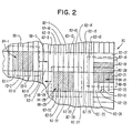
- the workpiece table is moved gradually to successive bridging positions so that while a subpattern is being written, the maximum writing field covers that associated subpattern writing field and when the abrupt shift from one subfield writing field to the next occurs, the maximum writing field bridges or covers both the present and the next subpattern writing field. In this way the maximum writing field always covers the subpattern writing field in use and allows an abrupt change to the next subpattern writing field without requiring the table (or the maximum writing field associated with it) to move.
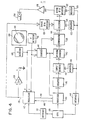
- Pattern data is continuously sent by the CPU to processor 140 as needed. If we assume that successive subpatterns will be shifted in the °X direction then "marker bits ("1" bits in the second bit position of X position data words) will appear in some of the X position words.
Landscapes
- Engineering & Computer Science (AREA)
- Chemical & Material Sciences (AREA)
- Nanotechnology (AREA)
- Crystallography & Structural Chemistry (AREA)
- Physics & Mathematics (AREA)
- Analytical Chemistry (AREA)
- Mathematical Physics (AREA)
- Theoretical Computer Science (AREA)
- Condensed Matter Physics & Semiconductors (AREA)
- General Physics & Mathematics (AREA)
- Manufacturing & Machinery (AREA)
- Exposure And Positioning Against Photoresist Photosensitive Materials (AREA)
- Laser Beam Processing (AREA)
- Electron Beam Exposure (AREA)
Applications Claiming Priority (2)
| Application Number | Priority Date | Filing Date | Title |
|---|---|---|---|
| US06/432,170 US4477729A (en) | 1982-10-01 | 1982-10-01 | Continuously writing electron beam stitched pattern exposure system |
| US432170 | 1982-10-01 |
Publications (3)
| Publication Number | Publication Date |
|---|---|
| EP0105214A2 true EP0105214A2 (fr) | 1984-04-11 |
| EP0105214A3 EP0105214A3 (en) | 1986-07-16 |
| EP0105214B1 EP0105214B1 (fr) | 1990-03-14 |
Family
ID=23715041
Family Applications (1)
| Application Number | Title | Priority Date | Filing Date |
|---|---|---|---|
| EP83108762A Expired EP0105214B1 (fr) | 1982-10-01 | 1983-09-06 | Méthode et dispositif pour écrire des motifs lithographique de grandes dimensions |
Country Status (4)
| Country | Link |
|---|---|
| US (1) | US4477729A (fr) |
| EP (1) | EP0105214B1 (fr) |
| JP (1) | JPS5970488A (fr) |
| DE (1) | DE3381335D1 (fr) |
Cited By (5)
| Publication number | Priority date | Publication date | Assignee | Title |
|---|---|---|---|---|
| EP0169561A3 (fr) * | 1984-07-26 | 1987-04-22 | The Perkin-Elmer Corporation | Stratégie pour la commande d'un instrument de microlithographie |
| EP0293823A3 (en) * | 1984-06-21 | 1989-07-12 | American Telephone And Telegraph Company | Deep-uv lithography |
| EP0327093A3 (en) * | 1988-02-04 | 1990-11-07 | Fujitsu Limited | Electron beam exposure method and apparatus |
| EP0397073A3 (fr) * | 1989-05-09 | 1991-09-11 | Olympus Optical Co., Ltd. | Appareil pour former un dessin de circuit utilisant un microscope à effet tunnel à balayage |
| EP0443249A3 (en) * | 1990-02-22 | 1992-02-26 | American Telephone And Telegraph Company | Manufacturing adjustment during article fabrication |
Families Citing this family (23)
| Publication number | Priority date | Publication date | Assignee | Title |
|---|---|---|---|---|
| JPS60196941A (ja) * | 1984-02-29 | 1985-10-05 | Fujitsu Ltd | 電子線露光方法 |
| US4837447A (en) * | 1986-05-06 | 1989-06-06 | Research Triangle Institute, Inc. | Rasterization system for converting polygonal pattern data into a bit-map |
| GB2190567A (en) * | 1986-05-16 | 1987-11-18 | Philips Electronic Associated | Electron beam pattern generator control |
| JPS63199421A (ja) * | 1987-02-16 | 1988-08-17 | Toshiba Corp | 荷電ビ−ム描画方法 |
| US4818885A (en) * | 1987-06-30 | 1989-04-04 | International Business Machines Corporation | Electron beam writing method and system using large range deflection in combination with a continuously moving table |
| IL97021A0 (en) * | 1991-01-24 | 1992-03-29 | Ibm Israel | Partitioning method for e-beam lithography |
| KR950002578B1 (ko) * | 1991-03-13 | 1995-03-23 | 후지쓰 가부시끼가이샤 | 전자빔 노광방법 |
| US5393987A (en) * | 1993-05-28 | 1995-02-28 | Etec Systems, Inc. | Dose modulation and pixel deflection for raster scan lithography |
| JPH09270375A (ja) * | 1996-03-29 | 1997-10-14 | Advantest Corp | 電子ビーム露光装置 |
| US5621216A (en) * | 1996-04-26 | 1997-04-15 | International Business Machines Corporation | Hardware/software implementation for multipass E-beam mask writing |
| US6130517A (en) * | 1998-02-12 | 2000-10-10 | Nikon Corporation | Magnetic actuator producing large acceleration on fine stage and low RMS power gain |
| US6259106B1 (en) * | 1999-01-06 | 2001-07-10 | Etec Systems, Inc. | Apparatus and method for controlling a beam shape |
| US6537052B1 (en) | 1999-08-23 | 2003-03-25 | Richard J. Adler | Method and apparatus for high speed electron beam rapid prototyping |
| DE102004055149B4 (de) * | 2004-11-16 | 2007-07-19 | Leica Microsystems Lithography Gmbh | Vorrichtung und Verfahren zum Abbilden eines Mehrfach-Partikelstrahls auf ein Substrat |
| ATE537550T1 (de) * | 2005-07-08 | 2011-12-15 | Nexgen Semi Holding Inc | Vorrichtung und verfahren zur kontrollierten fertigung von halbleitern mittels teilchenstrahlen |
| WO2008140585A1 (fr) | 2006-11-22 | 2008-11-20 | Nexgen Semi Holding, Inc. | Appareil et procédé de fabrication de masque conforme |
| US7687210B2 (en) * | 2007-06-25 | 2010-03-30 | International Business Machines Corporation | Space tolerance with stitching |
| JP5063320B2 (ja) * | 2007-12-11 | 2012-10-31 | 株式会社ニューフレアテクノロジー | 描画装置及び描画データの変換方法 |
| US10991545B2 (en) | 2008-06-30 | 2021-04-27 | Nexgen Semi Holding, Inc. | Method and device for spatial charged particle bunching |
| US10566169B1 (en) | 2008-06-30 | 2020-02-18 | Nexgen Semi Holding, Inc. | Method and device for spatial charged particle bunching |
| KR102787815B1 (ko) * | 2017-11-09 | 2025-03-27 | 에이에스엠엘 네델란즈 비.브이. | 리소그래피 장치 및 방법 |
| TR2022007784A2 (tr) * | 2022-05-13 | 2023-11-21 | Bilkent Ueniversitesi Ulusal Nanoteknoloji Arastirma Merkezi | Nano ölçekte bi̇r li̇tografi̇ yöntemi̇ |
| US12493005B1 (en) | 2022-06-07 | 2025-12-09 | Nexgen Semi Holding, Inc. | Extended range active illumination imager |
Family Cites Families (4)
| Publication number | Priority date | Publication date | Assignee | Title |
|---|---|---|---|---|
| US4132898A (en) * | 1977-11-01 | 1979-01-02 | Fujitsu Limited | Overlapping boundary electron exposure system method and apparatus |
| US4147937A (en) * | 1977-11-01 | 1979-04-03 | Fujitsu Limited | Electron beam exposure system method and apparatus |
| JPS5753938A (en) * | 1980-09-17 | 1982-03-31 | Toshiba Corp | Electron beam exposure apparatus |
| JPS5821422B2 (ja) * | 1980-12-26 | 1983-04-30 | 株式会社東芝 | 荷電ビ−ム露光装置 |
-
1982
- 1982-10-01 US US06/432,170 patent/US4477729A/en not_active Expired - Lifetime
-
1983
- 1983-07-20 JP JP58131120A patent/JPS5970488A/ja active Pending
- 1983-09-06 EP EP83108762A patent/EP0105214B1/fr not_active Expired
- 1983-09-06 DE DE8383108762T patent/DE3381335D1/de not_active Expired - Lifetime
Cited By (6)
| Publication number | Priority date | Publication date | Assignee | Title |
|---|---|---|---|---|
| EP0293823A3 (en) * | 1984-06-21 | 1989-07-12 | American Telephone And Telegraph Company | Deep-uv lithography |
| EP0169561A3 (fr) * | 1984-07-26 | 1987-04-22 | The Perkin-Elmer Corporation | Stratégie pour la commande d'un instrument de microlithographie |
| EP0327093A3 (en) * | 1988-02-04 | 1990-11-07 | Fujitsu Limited | Electron beam exposure method and apparatus |
| EP0397073A3 (fr) * | 1989-05-09 | 1991-09-11 | Olympus Optical Co., Ltd. | Appareil pour former un dessin de circuit utilisant un microscope à effet tunnel à balayage |
| US5216254A (en) * | 1989-05-09 | 1993-06-01 | Olympus Optical Co., Ltd. | Circuit pattern forming apparatus using mu-stm |
| EP0443249A3 (en) * | 1990-02-22 | 1992-02-26 | American Telephone And Telegraph Company | Manufacturing adjustment during article fabrication |
Also Published As
| Publication number | Publication date |
|---|---|
| US4477729A (en) | 1984-10-16 |
| EP0105214A3 (en) | 1986-07-16 |
| JPS5970488A (ja) | 1984-04-20 |
| DE3381335D1 (de) | 1990-04-19 |
| EP0105214B1 (fr) | 1990-03-14 |
Similar Documents
| Publication | Publication Date | Title |
|---|---|---|
| US4477729A (en) | Continuously writing electron beam stitched pattern exposure system | |
| JP2725020B2 (ja) | 電子ビーム露光装置 | |
| US6573516B2 (en) | Electron-beam lithography method and electron-beam lithography system | |
| US5866300A (en) | Method of and system for exposing pattern on object by charged particle beam | |
| EP0248588B1 (fr) | Système d'exposition par faisceau d'électrons | |
| US7705322B2 (en) | Charged-particle beam writing method | |
| JP2614884B2 (ja) | 電子ビーム露光方法及びその装置 | |
| JPH0324771B2 (fr) | ||
| US5030836A (en) | Method and apparatus for drawing patterns using an energy beam | |
| EP0431864B1 (fr) | Méthode de détection et d'ajustement des conditions d'exposition dans un système d'exposition par faisceau de particules chargées et un tel système | |
| US5759423A (en) | Electron beam writing method and apparatus for carrying out the same | |
| US7476881B2 (en) | Charged beam drawing apparatus and charged beam drawing method | |
| KR940010150B1 (ko) | 전자빔노광방법 및 그 장치 | |
| US20010028039A1 (en) | Method for directing an electron beam onto a target position on a substrate surface | |
| US4420691A (en) | Method of aligning electron beam apparatus | |
| EP0074238A2 (fr) | Méthode d'exposition utilisant un faisceau énergétique | |
| JP2003272996A (ja) | 重ね合わせ露光方法と露光装置 | |
| JP3175112B2 (ja) | 荷電粒子線露光方法 | |
| US5434795A (en) | Method of forming pattern having optical angle in charged particle exposure system | |
| KR102845695B1 (ko) | Uvw 스테이지의 회전 오차를 보정하는 방법 | |
| JP2706599B2 (ja) | 電子線描画方法とその装置 | |
| EP0169561A2 (fr) | Stratégie pour la commande d'un instrument de microlithographie | |
| US7525109B2 (en) | Method for writing a large-area closed curvilinear pattern with a cartesian electron beam writing system | |
| JP4056140B2 (ja) | 荷電粒子ビーム露光装置 | |
| JP3057208B2 (ja) | 回転対称図形描画方法及びその装置 |
Legal Events
| Date | Code | Title | Description |
|---|---|---|---|
| PUAI | Public reference made under article 153(3) epc to a published international application that has entered the european phase |
Free format text: ORIGINAL CODE: 0009012 |
|
| AK | Designated contracting states |
Designated state(s): DE FR GB |
|
| 17P | Request for examination filed |
Effective date: 19840823 |
|
| PUAL | Search report despatched |
Free format text: ORIGINAL CODE: 0009013 |
|
| AK | Designated contracting states |
Kind code of ref document: A3 Designated state(s): DE FR GB |
|
| 17Q | First examination report despatched |
Effective date: 19880420 |
|
| GRAA | (expected) grant |
Free format text: ORIGINAL CODE: 0009210 |
|
| AK | Designated contracting states |
Kind code of ref document: B1 Designated state(s): DE FR GB |
|
| REF | Corresponds to: |
Ref document number: 3381335 Country of ref document: DE Date of ref document: 19900419 |
|
| ET | Fr: translation filed | ||
| PLBE | No opposition filed within time limit |
Free format text: ORIGINAL CODE: 0009261 |
|
| STAA | Information on the status of an ep patent application or granted ep patent |
Free format text: STATUS: NO OPPOSITION FILED WITHIN TIME LIMIT |
|
| 26N | No opposition filed | ||
| PGFP | Annual fee paid to national office [announced via postgrant information from national office to epo] |
Ref country code: GB Payment date: 19950822 Year of fee payment: 13 |
|
| PGFP | Annual fee paid to national office [announced via postgrant information from national office to epo] |
Ref country code: FR Payment date: 19950911 Year of fee payment: 13 |
|
| PGFP | Annual fee paid to national office [announced via postgrant information from national office to epo] |
Ref country code: DE Payment date: 19950921 Year of fee payment: 13 |
|
| PG25 | Lapsed in a contracting state [announced via postgrant information from national office to epo] |
Ref country code: GB Effective date: 19960906 |
|
| PG25 | Lapsed in a contracting state [announced via postgrant information from national office to epo] |
Ref country code: FR Effective date: 19960930 |
|
| GBPC | Gb: european patent ceased through non-payment of renewal fee |
Effective date: 19960906 |
|
| PG25 | Lapsed in a contracting state [announced via postgrant information from national office to epo] |
Ref country code: DE Effective date: 19970603 |
|
| REG | Reference to a national code |
Ref country code: FR Ref legal event code: ST |
|
| REG | Reference to a national code |
Ref country code: FR Ref legal event code: ST |