EP0106152A2 - Semiconductor laser device - Google Patents
Semiconductor laser device Download PDFInfo
- Publication number
- EP0106152A2 EP0106152A2 EP83108998A EP83108998A EP0106152A2 EP 0106152 A2 EP0106152 A2 EP 0106152A2 EP 83108998 A EP83108998 A EP 83108998A EP 83108998 A EP83108998 A EP 83108998A EP 0106152 A2 EP0106152 A2 EP 0106152A2
- Authority
- EP
- European Patent Office
- Prior art keywords
- semiconductor layer
- conductivity type
- laser
- semiconductor
- layer
- Prior art date
- Legal status (The legal status is an assumption and is not a legal conclusion. Google has not performed a legal analysis and makes no representation as to the accuracy of the status listed.)
- Granted
Links
Images

Classifications
-
- H—ELECTRICITY
- H01—ELECTRIC ELEMENTS
- H01S—DEVICES USING THE PROCESS OF LIGHT AMPLIFICATION BY STIMULATED EMISSION OF RADIATION [LASER] TO AMPLIFY OR GENERATE LIGHT; DEVICES USING STIMULATED EMISSION OF ELECTROMAGNETIC RADIATION IN WAVE RANGES OTHER THAN OPTICAL
- H01S5/00—Semiconductor lasers
- H01S5/20—Structure or shape of the semiconductor body to guide the optical wave ; Confining structures perpendicular to the optical axis, e.g. index or gain guiding, stripe geometry, broad area lasers, gain tailoring, transverse or lateral reflectors, special cladding structures, MQW barrier reflection layers
- H01S5/22—Structure or shape of the semiconductor body to guide the optical wave ; Confining structures perpendicular to the optical axis, e.g. index or gain guiding, stripe geometry, broad area lasers, gain tailoring, transverse or lateral reflectors, special cladding structures, MQW barrier reflection layers having a ridge or stripe structure
- H01S5/223—Buried stripe structure
- H01S5/2232—Buried stripe structure with inner confining structure between the active layer and the lower electrode
-
- H—ELECTRICITY
- H01—ELECTRIC ELEMENTS
- H01S—DEVICES USING THE PROCESS OF LIGHT AMPLIFICATION BY STIMULATED EMISSION OF RADIATION [LASER] TO AMPLIFY OR GENERATE LIGHT; DEVICES USING STIMULATED EMISSION OF ELECTROMAGNETIC RADIATION IN WAVE RANGES OTHER THAN OPTICAL
- H01S5/00—Semiconductor lasers
- H01S5/20—Structure or shape of the semiconductor body to guide the optical wave ; Confining structures perpendicular to the optical axis, e.g. index or gain guiding, stripe geometry, broad area lasers, gain tailoring, transverse or lateral reflectors, special cladding structures, MQW barrier reflection layers
- H01S5/22—Structure or shape of the semiconductor body to guide the optical wave ; Confining structures perpendicular to the optical axis, e.g. index or gain guiding, stripe geometry, broad area lasers, gain tailoring, transverse or lateral reflectors, special cladding structures, MQW barrier reflection layers having a ridge or stripe structure
- H01S5/223—Buried stripe structure
- H01S5/2232—Buried stripe structure with inner confining structure between the active layer and the lower electrode
- H01S5/2234—Buried stripe structure with inner confining structure between the active layer and the lower electrode having a structured substrate surface
Definitions
- the present invention relates to semiconductor laser devices, and more particularly to a semiconductor laser device which oscillates in a single longitudinal mode.
- the so-called BH (Buried Hetero) type or CSP (Channeled Substrate Planar) type laser which is a typical example of a semiconductor laser of the index-guided type, exhibits a good 'optical output-versus-current' characteristic and is free from astigmatism, and is therefore used as a pickup light source for an optical disk.
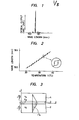
- the laser presents a single longitudinal mode oscillation in which most of its optical output concentrates in a single longitudinal mode, and which corresponds to a spectrum as shown in Figure 1 by way of example. It has been revealed, however, that when the ambient temperature has changed, a plurality of longitudinal modes oscillate simultaneously and cause severe noise in some devices, so the control and readout of the optical disk are hampered.
- the BH laser is introduced by:
- An object of the present invention is to provide a semiconductor laser device which oscillates in a single longitudinal mode and which is free from the noise as stated above.
- the present invention consists in improvements in a semiconductor laser of a conventional double heterostructure, namely, a semiconductor laser having at least a first semiconductor layer, and second and third semiconductor layers Which hold the first semiconductor layer therebetween and which are greater in the band gap and smaller in the refractive index than the first semiconductor layer.
- the oscillation in a single longitudinal mode is realized by employing the index-guided type as the' guide setup of an active region.
- the second and third semiconductor layers have opposite conductivity types.
- the relationship between the donor concentration (N D x 10 17 cm -3 ) of the semiconductor layer having the n-conductivity type in the second and third semiconductor layers of such semiconductor laser and the proportion ( ⁇ n (%)) of the optical output existing in the particular semiconductor layer relative to the total optical output of the laser is set at: whereby the aforementioned object can be accomplished.
- Te tellurium which develops a deep level exhibitive of saturable optical absorption is the most useful.
- the object of the present invention is achieved by setting the relationship between the donor concentration (N D x 10 17 cm -3 ) of the semiconductor layer having the n-conductivity type in the second or third semiconductor layer of the semiconductor laser and the proportion ( ⁇ n .(%)) of the optical output existing in the particular semiconductor layer relative to the total optical output of the laser, at N D ⁇ ⁇ n 500.
- DX centers Donor Complex Centers
- DX centers Donor Complex Centers
- the difference ⁇ of absorption losses arises among a longitudinal mode which oscillates and the other ncn-oscillating longitudinal modes, and the longitudinal modes other than the oscillating longitudinal mode suffer heavier losses, so that the oscillation in the single longitudinal mode is stabilized.
- a hysteresis as shown in Figure 2 contributes to the temperature variation of the longitudinal mode.
- the density of DX centers is substantially proportional to the donor density n. Accordingly, letting ⁇ n denote the percentage of the light distribution existing in the n-clad layer, the loss difference ⁇ has the following relationship:
- ⁇ n is calculated in accordance with a formula mentioned below.
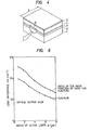
- Figure 3 is a diagram showing this model, in which n 23 n 3 and n 4 indicate the refractive indicies of the respective layers.
- numeral 2 designates a clad layer of the n-conductivity type
- numeral 3 an active layer
- numeral 4 a clad layer of the p-conductivity type.
- ⁇ n denotes the percentage of the light distribution existing in the n-clad layer.
- Ey 2 , E y3 and E Y4 denote electric field intensities in the respective layers 2, 3 and 4.
- d 3 denotes the thickness of the active layer 3.
- the electric field intensities E y2 , E y3 and E y4 in the above formula giving the proportion ⁇ n can be determined by solving characteristic equations whose parameters are the oscillation wavelength ( ⁇ ) of the laser, the thickness (d 3 ) of the active layer and the refractive indices n 2 , n 3 and n 4 of the respective layers.
- the indices n 2 , n 3 and n 4 can be evaluated from the wavelength ( ⁇ ) and the AlAs mole fractions of the respective layers. This is explained in, e. g., M. A. Afromowitz: Solid State Commun. 15 (1974) 59.
- the adjustment of the donor density is, of course, made by adjusting the quantity of doping with a donor impurity.
- the upper limit of the donor density is on the order of 2 x 10 18 cm -3 in view of the occurrence of lattice defects, etc.
- the adjustment of ⁇ n can be made by adjusting the thickness of the active layer, changing the ratios of the mole fractions of the two clad layers holding the active layer therebetween, etc.
- the loss difference ⁇ has dependencies upon the cavity length L of the laser and the width of a light emitting region, i. e., the width w of the active region.
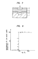
- Figure 4 shows how to take l and w by way of example. It exemplifies an index-guided type semiconductor laser which is usually termed a CSP (Channeled Substrate Planar type) laser.
- CSP Channelled Substrate Planar type
- numeral 1 designates a semiconductor substrate, numerals 2 and 4 clad layers, numeral 3 an active layer, and numeral 5 a cap layer.
- the index-guided structure is realized by utilizing the difference of effective refractive indices produced by the ruggedness of the clad layers.
- Figures 5 and 6 illustrate the relationship between the cavity length (l) and the loss difference and the relationship between the width of the active region and the loss difference, respectively.
- the loss difference presents a curve which has maximum values at some values of l. It is also understood from Figure 6 that the loss difference ⁇ becomes greater as the active region width w is smaller. In the present invention, accordingly, it is more favorable to set the product D n ⁇ n at or above 500 ( x 10 1 7 cm -3 .%) and to simultaneously optimize the laser cavity length l and the active region width w to the end of increasing the loss difference ⁇ .
- Results in Figure 5 were obtained as to examples in each of which the thickness of the active layer was 0.06 ⁇ m, the width of the active layer was 4 ⁇ m and the n carrier concentration was 1 x 10 18 cm -3 .
- n/p clad compositions when Ga 1-x Al x As denotes the composition of each clad layer, the ratio between the mole fraction (x) of the n-conductivity type clad layer and that (x') of the p-conductivity type clad layer is indicated. Results in Figure 6 were obtained as to examples in each of which the thickness of the active layer was 0.06 ⁇ m, the cavity length was 300 ⁇ m and the n carrier concentration was 1 x 1018 cm-3.
- the CSP type structure shown in Figure 4 was used as the index-guided type structure oscillating in a single longitudinal mode.
- a photoresist film having a window was formed by a conventional photoresist process. By performing chemical etching through the window, a recess about 1 ⁇ m deep was formed in the substrate 1.
- a Te-doped n-Al x Ga 1-x As clad layer 2 (0.4 ⁇ x ⁇ 0.45), an undoped AlyGa l-y As active layer 3 (y ⁇ 0.14, corresponding to the oscillation wavelength of 780 nm), a Zn-doped p-Al z Ga 1-z As clad layer 4 (0.4 ⁇ z ⁇ 0.5, p ⁇ 5 x 10 17 cm -3 ), and a Te-doped n-GaAs cap layer 5 (n ⁇ 1 x 10 18 cm -3 ) were formed on the substrate by the well-known continuous liquid epitaxy.
- the thickness of the active layer 3 was 0.04 - 0.07 ⁇ m
- the thickness of the n-clad layer 2 was 1.3 ⁇ m at the middle part of the recess and 0.3 ⁇ m on both the sides of the recess
- the thickness of the p-clad layer 4 was 1.5 ⁇ m
- the thickness of the cap layer 5 was 1 ⁇ m.
- Table 1 lists up examples of the semiconductor laser manufactured by way of trial. All the examples wrere excellent in noise characteristics.
- Figure 7 shows a structure of the type in which the active layer is curved, as an embodiment corresponding to Figure 2.
- the active layer sags slightly at the middle part of the recess, and the thickness of the active layer at its central part is slightly greater, so that a transverse mode is controlled.
- Numerals 1-5 in Figure 7 are similar to those in the case of the CSP structure in Figure 4.
- an Si0 2 -SiN film was formed by the sputtering evaporation, or an SiO 2 -Al 2 O 3 film by the CVD (Chemical Vapor Deposition).
- CVD Chemical Vapor Deposition
- Ti-Mo-Au was evaporated as a p-type electrode, and AuGeNi-Cr-Pd-Au as an n-type electrode.
- the crystal was cleaved at the (110) faces so that the opposing faces might become parallel to each other. Then, the laser device was finished up.
- the quantity of doping with Te was changed in a range of 1 - 20 x 10 17 cm- 3 in terms of the carrier density n.
- the mole ratio (x/z) of AlAs between the n-conductivity type and p-conductivity type clad layers was changed into the four sorts: (0.4/0.4), (0.4/0.45), (0.45/0.45) and (0.45/0.50).
- the thickness d of the active layer was changed in a range of 0.04 - 0.07 ⁇ m, whereby ⁇ n was changed in a range of 40 - 70 %.
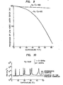
- the noise characteristics of laser devices produced on the basis of the combinations of these values N D and ⁇ n were investigated. As a result, it has been revealed that the available percentage of low noise devices is correlated with the product ND, ⁇ n very well as illustrated in Figure 8. That is, it has been revealed that, with the devices satisfying N D . ⁇ n ⁇ 500, low noise can be realized at the available percentage of 100 %.
- the width of the active region was 4 ⁇ m, and the cavity length was 300 rm.
- Figure 9 illustrates the temperature dependencies of the percentages of the low noise devices as to the device groups of ND .
- ⁇ n 400 and 500 among the devices shown in Figure 8.
- the available percentage lowers in correspondence with the fact that the coefficient of light absorption by the DX centers decreases.
- the devices of N D ⁇ ⁇ n ⁇ 500 it is seen that a high available percentage above 90 % can be attained at temperatures up to 50 - 60 °C.
- changes in the noise characteristics based on the following changes in parameters were studied:
- the thickness d of the active layer was changed in a range of 0.04 - 0.07 ⁇ m.
- the laser cavity length was changed in a range of 100 - 500 ⁇ m, and the active layer width w was changed in a range of 1 - 8 ⁇ m, whereupon the noise characteristics of the laser devices were investigated.
- the results were that the devices whose cavity lengths l lay within ranges of 210 - 250 and 400 - 440 fm were less in the temperature noise and simultaneously higher in the available percentage of low noise devices than the devices whose cavity lengths t lay outside the ranges.
- the wavelength is not restricted to 780 nm, but similar results have been obtained over the whole range of wavelengths of 680 nm to 890 nm, over which AlGaAs-based lasers are capable of CW oscillations.
- the invention is not restricted to lasers fabricated by the liquid epitaxy, but substantially the same results are obtained as to an MBE-grown device having an Sn- or Si-doped clad layer and a device fabricated by an Mo-CVD process and having an Se- or S-doped clad layer.
- the contents of the present invention have been similarly effective in semiconductor laser devices employing laser materials other than AlGaAs, for example, semiconductor laser devices employing group-III - V semiconductor materials such as InGaAsP-based lasers of wavelengths of 1.2 - 1.6 f m.
- Semiconductor laser devices of a single longitudinal mode can be stably provided by applying the present invention.
- Figure 10 illustrates the RIN (Relative Intensity Noise) of semiconductor laser devices while comparing an example to which the present invention is applied, with an example to which it is not applied.
- the results have been obtained under the conditions of an output of 3 mW, a measurement frequency (f) of 2 - 12 MHz and a measurement bandwidth ( ⁇ f) of 300 kHz.
- the general items of the RIN are detailed in, e. g., a paper by K. Petermann and E. Weidel contained in IEEE, QE-17, No. 7, 1981, p. 1251.
Landscapes
- Physics & Mathematics (AREA)
- Geometry (AREA)
- Condensed Matter Physics & Semiconductors (AREA)
- General Physics & Mathematics (AREA)
- Electromagnetism (AREA)
- Optics & Photonics (AREA)
- Semiconductor Lasers (AREA)
Abstract
Description
- The present invention relates to semiconductor laser devices, and more particularly to a semiconductor laser device which oscillates in a single longitudinal mode.
- The so-called BH (Buried Hetero) type or CSP (Channeled Substrate Planar) type laser, which is a typical example of a semiconductor laser of the index-guided type, exhibits a good 'optical output-versus-current' characteristic and is free from astigmatism, and is therefore used as a pickup light source for an optical disk. The laser presents a single longitudinal mode oscillation in which most of its optical output concentrates in a single longitudinal mode, and which corresponds to a spectrum as shown in Figure 1 by way of example. It has been revealed, however, that when the ambient temperature has changed, a plurality of longitudinal modes oscillate simultaneously and cause severe noise in some devices, so the control and readout of the optical disk are hampered.
- The CSP laser is reported in detail in :
- (1) IEEE Journal of Quantum Electronics, vol. QE-14, No. 2, Feb. 1978, pp. 89 - 94,
- (2) J. Appl. Phys. 49(9), Sept. 1978, pp. 4644 - 4648, etc.
- The BH laser is introduced by:
- IEEE Journal of Quantum Electronics, vol. QE-11, No. 7, July 1975,
etc. - An object of the present invention is to provide a semiconductor laser device which oscillates in a single longitudinal mode and which is free from the noise as stated above.
- The present invention consists in improvements in a semiconductor laser of a conventional double heterostructure, namely, a semiconductor laser having at least a first semiconductor layer, and second and third semiconductor layers Which hold the first semiconductor layer therebetween and which are greater in the band gap and smaller in the refractive index than the first semiconductor layer. Usually, the oscillation in a single longitudinal mode is realized by employing the index-guided type as the' guide setup of an active region. Ordinarily, the second and third semiconductor layers have opposite conductivity types. The relationship between the donor concentration (ND x 1017 cm-3) of the semiconductor layer having the n-conductivity type in the second and third semiconductor layers of such semiconductor laser and the proportion (Γn (%)) of the optical output existing in the particular semiconductor layer relative to the total optical output of the laser is set at:

- As a donor impurity, Te (tellurium) which develops a deep level exhibitive of saturable optical absorption is the most useful.
- In the accompanying drawings:
- Figure 1 shows a typical longitudinal mode spectrum distribution of an index-guided type semiconductor laser device which oscillates in a single longitudinal mode;
- Figure 2 is a graph showing a typical example of the temperature dependency of the oscillation wavelength observed in a semiconductor laser device in which a single longitudinal mode oscillation is stabilized;
- .Figure 3 is a model diagram for explaining the concept of the proportion of a light distribution existent in a clad layer;
- Figure 4 is a perspective view of a CSP type laser device;
- . Figure 5 is a graph showing the relationship between the-loss difference Δα and the cavity length;
- Figure 6 is a graph showing the relationship between the loss difference and the width of the active layer;
- Figure ? is a sectional view showing an index-guided type semiconductor laser device whose active layer is curved;
- Figure 8 is a graph showing the relationship between ND·Γn and the available percentage of low noise devices;
- Figure 9 is a graph showing the temperature dependency of the percentage of low noise laser devices; and
- Figure 10 is a graph showing the temperature dependency of RIN (relative intensity noise).
- As stated before, the object of the present invention is achieved by setting the relationship between the donor concentration (ND x 1017 cm-3) of the semiconductor layer having the n-conductivity type in the second or third semiconductor layer of the semiconductor laser and the proportion (Γn .(%)) of the optical output existing in the particular semiconductor layer relative to the total optical output of the laser, at ND· Γn 500.
- The principle is interpreted as follows. Deep trap levels exhibitive of saturable optical absorption, called DX centers (Donor Complex Centers), are developed in a suitable amount within the n-conductivity type clad layer of the semiconductor laser, whereupon a suitable proportion of the total optical output is caused to exist within the n-conductivity type clad layer. Under such conditions, the difference Δα of absorption losses arises among a longitudinal mode which oscillates and the other ncn-oscillating longitudinal modes, and the longitudinal modes other than the oscillating longitudinal mode suffer heavier losses, so that the oscillation in the single longitudinal mode is stabilized. Further, a hysteresis as shown in Figure 2 contributes to the temperature variation of the longitudinal mode. Only the mode of one wavelength can rise at an identical temperature, and the longitudinal mode is stabilized. It is considered that, as the loss difference Δα is greater, the longitudinal mode will -become more difficult to vary against temperature changes, and noise arising due to the longitudinal mode variation attributed to temperature fluctuations will decrease more. Figure 2 depicts small hysteresis characteristics with temperature differences of one degree odd, and the above-stated influence of the changes of the ambient temperature on the mode concerns such extent of temperature differences.
- Usually, in case of doping a semiconductor layer with a donor impurity, the density of DX centers is substantially proportional to the donor density n. Accordingly, letting Γn denote the percentage of the light distribution existing in the n-clad layer, the loss difference Δα has the following relationship:

- Using a three-layer waveguide line model, Γn is calculated in accordance with a formula mentioned below. Figure 3 is a diagram showing this model, in which n23 n3 and n4 indicate the refractive indicies of the respective layers. In the figure,
numeral 2 designates a clad layer of the n-conductivity type,numeral 3 an active layer, and numeral 4 a clad layer of the p-conductivity type. Γn denotes the percentage of the light distribution existing in the n-clad layer.
respective layers active layer 3. - The electric field intensities Ey2, Ey3 and Ey4 in the above formula giving the proportion Γn can be determined by solving characteristic equations whose parameters are the oscillation wavelength (λ) of the laser, the thickness (d3) of the active layer and the refractive indices n2, n3 and n4 of the respective layers. In addition, the indices n2, n3 and n4 can be evaluated from the wavelength (λ) and the AlAs mole fractions of the respective layers. This is explained in, e. g., M. A. Afromowitz: Solid State Commun. 15 (1974) 59.
- The fundamental idea of such waveguide line model is as explained in, e. g., 'Semiconductor Lasers and Heterostructure LEDS, HENRY KRESSEL et al, ACADEMIC PRESS, New York 1977', pp. 148 - 150.
- The aforementioned relationship can be set by various methods as stated below.
- The adjustment of the donor density is, of course, made by adjusting the quantity of doping with a donor impurity. The upper limit of the donor density is on the order of 2 x 1018 cm-3 in view of the occurrence of lattice defects, etc.
- Further, the adjustment of Γn can be made by adjusting the thickness of the active layer, changing the ratios of the mole fractions of the two clad layers holding the active layer therebetween, etc. Besides, the loss difference Δα has dependencies upon the cavity length L of the laser and the width of a light emitting region, i. e., the width w of the active region. Figure 4 shows how to take ℓ and w by way of example. It exemplifies an index-guided type semiconductor laser which is usually termed a CSP (Channeled Substrate Planar type) laser.
- In Figure 4, numeral 1 designates a semiconductor substrate,
numerals numeral 3 an active layer, and numeral 5 a cap layer. The index-guided structure is realized by utilizing the difference of effective refractive indices produced by the ruggedness of the clad layers. - Figures 5 and 6 illustrate the relationship between the cavity length (ℓ) and the loss difference and the relationship between the width of the active region and the loss difference, respectively.
- It is understood from Figure 5 that the loss difference presents a curve which has maximum values at some values of ℓ. It is also understood from Figure 6 that the loss difference Δα becomes greater as the active region width w is smaller. In the present invention, accordingly, it is more favorable to set the product Dn·Γn at or above 500 (x 10 17 cm-3.%) and to simultaneously optimize the laser cavity length ℓ and the active region width w to the end of increasing the loss difference Δα. Results in Figure 5 were obtained as to examples in each of which the thickness of the active layer was 0.06 µm, the width of the active layer was 4 µm and the n carrier concentration was 1 x 1018 cm-3. Regarding n/p clad compositions, when Ga1-x AlxAs denotes the composition of each clad layer, the ratio between the mole fraction (x) of the n-conductivity type clad layer and that (x') of the p-conductivity type clad layer is indicated. Results in Figure 6 were obtained as to examples in each of which the thickness of the active layer was 0.06 µm, the cavity length was 300 µm and the n carrier concentration was 1 x 1018 cm-3.
- In both Figures 5 and 6, the structure in which the mole fraction of the p-type clad layer is greater than that of the n-type clad layer has a greater loss difference Δα as compared with the structure in which the mole fractions of both the layers are equal. The reason is that, in the former structure, the refractive index n4 in Figure 3 becomes smaller than n2, so the light distribution shifts toward the n-type clad layer to increase Γn.
- Now, the present invention will be described in detail with reference to embodiments thereof.
- In an AlGaAs-based visible semiconductor laser having an oscillation wavelength of 780 nm, the CSP type structure shown in Figure 4 was used as the index-guided type structure oscillating in a single longitudinal mode. On the (100) face of an n-type GaAs substrate 1 (doped with Si, n ~ 1 x 1018 cm-3), a photoresist film having a window was formed by a conventional photoresist process. By performing chemical etching through the window, a recess about 1 µm deep was formed in the substrate 1. After removing the photoresist film, a Te-doped n-AlxGa1-xAs clad layer 2 (0.4 ≤ x ≤ 0.45), an undoped AlyGal-yAs active layer 3 (y ~ 0.14, corresponding to the oscillation wavelength of 780 nm), a Zn-doped p-AlzGa1-z As clad layer 4 (0.4 ≤ z ≤ 0.5, p ~ 5 x 1017 cm-3 ), and a Te-doped n-GaAs cap layer 5 (n ~1 x 1018 cm-3) were formed on the substrate by the well-known continuous liquid epitaxy. At this time, the thickness of the
active layer 3 was 0.04 - 0.07 µm, the thickness of the n-cladlayer 2 was 1.3 µm at the middle part of the recess and 0.3 µm on both the sides of the recess, the thickness of the p-cladlayer 4 was 1.5 µm, and the thickness of thecap layer 5 was 1 µm. Table 1 lists up examples of the semiconductor laser manufactured by way of trial.
cap layer 5, an Si02-SiN film was formed by the sputtering evaporation, or an SiO2-Al2O3 film by the CVD (Chemical Vapor Deposition). Thereafter, via the photoresist process, a diffusion window was provided, through which Zn was diffused to form a p-type Zn-diffusedregion 6 serving as a current path. Thereafter, Ti-Mo-Au was evaporated as a p-type electrode, and AuGeNi-Cr-Pd-Au as an n-type electrode. Lastly, the crystal was cleaved at the (110) faces so that the opposing faces might become parallel to each other. Then, the laser device was finished up. - Herein, in order to change the DX center density in the n-clad layer, the quantity of doping with Te was changed in a range of 1 - 20 x 1017 cm-3 in terms of the carrier density n. Besides, in order to change the percentage Γn of the optical output in the n-clad layer, the mole ratio (x/z) of AlAs between the n-conductivity type and p-conductivity type clad layers was changed into the four sorts: (0.4/0.4), (0.4/0.45), (0.45/0.45) and (0.45/0.50). Further, the thickness d of the active layer was changed in a range of 0.04 - 0.07 µm, whereby Γn was changed in a range of 40 - 70 %. The noise characteristics of laser devices produced on the basis of the combinations of these values ND and Γn were investigated. As a result, it has been revealed that the available percentage of low noise devices is correlated with the product ND,Γn very well as illustrated in Figure 8. That is, it has been revealed that, with the devices satisfying ND . Γn ≥ 500, low noise can be realized at the available percentage of 100 %. In each of the examples, the width of the active region was 4 µm, and the cavity length was 300 rm. Figure 9 illustrates the temperature dependencies of the percentages of the low noise devices as to the device groups of ND . Γn = 400 and 500 among the devices shown in Figure 8. At high temperatures, the available percentage lowers in correspondence with the fact that the coefficient of light absorption by the DX centers decreases. As regards the devices of ND · Γn ≥ 500, however, it is seen that a high available percentage above 90 % can be attained at temperatures up to 50 - 60 °C. Further, changes in the noise characteristics based on the following changes in parameters were studied:
- (1) The thickness d of the active layer was changed in a range of 0.04 - 0.07 µm. (2) Among devices which had equal values of ND· Γn, the laser cavity length was changed in a range of 100 - 500 µm, and the active layer width w was changed in a range of 1 - 8 µm, whereupon the noise characteristics of the laser devices were investigated. The results were that the devices whose cavity lengths ℓ lay within ranges of 210 - 250 and 400 - 440 fm were less in the temperature noise and simultaneously higher in the available percentage of low noise devices than the devices whose cavity lengths t lay outside the ranges. These results were basically the same as shown in Figure 5. It was also found that the devices whose active layer widths w were smaller were less in the noise and higher in the available percentage of low noise devices. These results were basically the same as shown in Figure 6. It has accordingly been revealed very favorable to set the laser cavity length ℓ within the range of 210 - 250 µm and the active layer width w within a range of 1 - 4 µm under the condition of ND · Γn ≥ 500.
- While, in the above, the description has been made by taking as examples a semiconductor laser of the CSP type and a semiconductor laser of the CSP type having a curved active layer, it is needless to say that quite similar results are obtained as to other lasers including a transverse mode index-guided type semiconductor laser, a BH (Buried Heterostructure) laser, a TS (Terraced Substrate) laser, a VSIS laser, and a TJS (Transverse Junction Strip) laser. In addition, the wavelength is not restricted to 780 nm, but similar results have been obtained over the whole range of wavelengths of 680 nm to 890 nm, over which AlGaAs-based lasers are capable of CW oscillations. Besides, the invention is not restricted to lasers fabricated by the liquid epitaxy, but substantially the same results are obtained as to an MBE-grown device having an Sn- or Si-doped clad layer and a device fabricated by an Mo-CVD process and having an Se- or S-doped clad layer. Moreover, the contents of the present invention have been similarly effective in semiconductor laser devices employing laser materials other than AlGaAs, for example, semiconductor laser devices employing group-III - V semiconductor materials such as InGaAsP-based lasers of wavelengths of 1.2 - 1.6 fm.
- Semiconductor laser devices of a single longitudinal mode can be stably provided by applying the present invention.
- Figure 10 illustrates the RIN (Relative Intensity Noise) of semiconductor laser devices while comparing an example to which the present invention is applied, with an example to which it is not applied. The results have been obtained under the conditions of an output of 3 mW, a measurement frequency (f) of 2 - 12 MHz and a measurement bandwidth (Δf) of 300 kHz. The general items of the RIN are detailed in, e. g., a paper by K. Petermann and E. Weidel contained in IEEE, QE-17, No. 7, 1981, p. 1251.
- As apparent from the figure, low noise can be maintained at any temperature in accordance with the application of the present invention. In contrast, when the present invention is not applied, noise versus temperature characteristics become very unstable.
Claims (3)
Applications Claiming Priority (2)
| Application Number | Priority Date | Filing Date | Title |
|---|---|---|---|
| JP158136/82 | 1982-09-13 | ||
| JP57158136A JPS5947790A (en) | 1982-09-13 | 1982-09-13 | Semiconductor laser device |
Publications (3)
| Publication Number | Publication Date |
|---|---|
| EP0106152A2 true EP0106152A2 (en) | 1984-04-25 |
| EP0106152A3 EP0106152A3 (en) | 1986-03-05 |
| EP0106152B1 EP0106152B1 (en) | 1989-08-09 |
Family
ID=15665055
Family Applications (1)
| Application Number | Title | Priority Date | Filing Date |
|---|---|---|---|
| EP83108998A Expired EP0106152B1 (en) | 1982-09-13 | 1983-09-12 | Semiconductor laser device |
Country Status (4)
| Country | Link |
|---|---|
| US (1) | US4563764A (en) |
| EP (1) | EP0106152B1 (en) |
| JP (1) | JPS5947790A (en) |
| DE (1) | DE3380387D1 (en) |
Families Citing this family (4)
| Publication number | Priority date | Publication date | Assignee | Title |
|---|---|---|---|---|
| JPS6140027A (en) * | 1984-07-31 | 1986-02-26 | Matsushita Electric Ind Co Ltd | Crystal growth method |
| US5075743A (en) * | 1989-06-06 | 1991-12-24 | Cornell Research Foundation, Inc. | Quantum well optical device on silicon |
| JP3278951B2 (en) * | 1992-10-23 | 2002-04-30 | ソニー株式会社 | Method of forming ohmic electrode |
| US5537433A (en) * | 1993-07-22 | 1996-07-16 | Sharp Kabushiki Kaisha | Semiconductor light emitter |
Family Cites Families (6)
| Publication number | Priority date | Publication date | Assignee | Title |
|---|---|---|---|---|
| JPS5252999Y2 (en) * | 1972-04-18 | 1977-12-01 | ||
| JPS49120992U (en) * | 1973-02-13 | 1974-10-16 | ||
| CA1147045A (en) * | 1978-09-20 | 1983-05-24 | Naoki Chinone | Semiconductor laser device |
| CA1137605A (en) * | 1979-01-15 | 1982-12-14 | Donald R. Scifres | High output power laser |
| US4280106A (en) * | 1979-05-15 | 1981-07-21 | Xerox Corporation | Striped substrate planar laser |
| JPS5640292A (en) * | 1979-09-11 | 1981-04-16 | Fujitsu Ltd | Semiconductor laser |
-
1982
- 1982-09-13 JP JP57158136A patent/JPS5947790A/en active Granted
-
1983
- 1983-09-12 DE DE8383108998T patent/DE3380387D1/en not_active Expired
- 1983-09-12 EP EP83108998A patent/EP0106152B1/en not_active Expired
- 1983-09-13 US US06/531,710 patent/US4563764A/en not_active Expired - Lifetime
Also Published As
| Publication number | Publication date |
|---|---|
| EP0106152B1 (en) | 1989-08-09 |
| DE3380387D1 (en) | 1989-09-14 |
| US4563764A (en) | 1986-01-07 |
| EP0106152A3 (en) | 1986-03-05 |
| JPS5947790A (en) | 1984-03-17 |
| JPH0422033B2 (en) | 1992-04-15 |
Similar Documents
| Publication | Publication Date | Title |
|---|---|---|
| US4755015A (en) | Monolithic integrated semiconductor device of semiconductor laser and optical waveguide | |
| US4404678A (en) | Semiconductor laser device | |
| US4128815A (en) | Single transverse mode operation in double heterostructure junction laser | |
| DE69032451T2 (en) | Semiconductor laser and method of manufacturing the same | |
| US4425650A (en) | Buried heterostructure laser diode | |
| EP0488820B1 (en) | Optical semiconductor device | |
| US4257011A (en) | Semiconductor laser device | |
| US4426702A (en) | Semiconductor laser device | |
| US5289484A (en) | Laser diode | |
| US4575919A (en) | Method of making heteroepitaxial ridge overgrown laser | |
| JP2004179274A (en) | Optical semiconductor device | |
| US5260959A (en) | Narrow beam divergence laser diode | |
| US4329660A (en) | Semiconductor light emitting device | |
| US5361271A (en) | Semiconductor laser | |
| JP2553731B2 (en) | Semiconductor optical device | |
| JPH05226789A (en) | Products containing strained layer quantum well lasers | |
| US4416012A (en) | W-Guide buried heterostructure laser | |
| EP0843393B1 (en) | Semiconductor laser diode | |
| JPS589389A (en) | Light emitting structure and method of producing same | |
| US4622673A (en) | Heteroepitaxial ridge overgrown laser | |
| US5420066A (en) | Method for producing semiconductor laser device using etch stop layer | |
| Kaminow et al. | Low threshold ridge waveguide laser at 1.55 μm | |
| US5524017A (en) | Quantum well semiconductor laser | |
| EP0106152B1 (en) | Semiconductor laser device | |
| US5756373A (en) | Method for fabricating optical semiconductor device |
Legal Events
| Date | Code | Title | Description |
|---|---|---|---|
| PUAI | Public reference made under article 153(3) epc to a published international application that has entered the european phase |
Free format text: ORIGINAL CODE: 0009012 |
|
| AK | Designated contracting states |
Designated state(s): DE FR GB NL |
|
| 17P | Request for examination filed |
Effective date: 19841220 |
|
| PUAL | Search report despatched |
Free format text: ORIGINAL CODE: 0009013 |
|
| AK | Designated contracting states |
Kind code of ref document: A3 Designated state(s): DE FR GB NL |
|
| 17Q | First examination report despatched |
Effective date: 19871203 |
|
| GRAA | (expected) grant |
Free format text: ORIGINAL CODE: 0009210 |
|
| AK | Designated contracting states |
Kind code of ref document: B1 Designated state(s): DE FR GB NL |
|
| REF | Corresponds to: |
Ref document number: 3380387 Country of ref document: DE Date of ref document: 19890914 |
|
| ET | Fr: translation filed | ||
| PLBE | No opposition filed within time limit |
Free format text: ORIGINAL CODE: 0009261 |
|
| STAA | Information on the status of an ep patent application or granted ep patent |
Free format text: STATUS: NO OPPOSITION FILED WITHIN TIME LIMIT |
|
| 26N | No opposition filed | ||
| PGFP | Annual fee paid to national office [announced via postgrant information from national office to epo] |
Ref country code: GB Payment date: 19960902 Year of fee payment: 14 |
|
| PGFP | Annual fee paid to national office [announced via postgrant information from national office to epo] |
Ref country code: FR Payment date: 19960916 Year of fee payment: 14 |
|
| PGFP | Annual fee paid to national office [announced via postgrant information from national office to epo] |
Ref country code: NL Payment date: 19960930 Year of fee payment: 14 |
|
| PGFP | Annual fee paid to national office [announced via postgrant information from national office to epo] |
Ref country code: DE Payment date: 19961126 Year of fee payment: 14 |
|
| PG25 | Lapsed in a contracting state [announced via postgrant information from national office to epo] |
Ref country code: GB Free format text: LAPSE BECAUSE OF NON-PAYMENT OF DUE FEES Effective date: 19970912 |
|
| PG25 | Lapsed in a contracting state [announced via postgrant information from national office to epo] |
Ref country code: FR Free format text: THE PATENT HAS BEEN ANNULLED BY A DECISION OF A NATIONAL AUTHORITY Effective date: 19970930 |
|
| PG25 | Lapsed in a contracting state [announced via postgrant information from national office to epo] |
Ref country code: NL Free format text: LAPSE BECAUSE OF NON-PAYMENT OF DUE FEES Effective date: 19980401 |
|
| GBPC | Gb: european patent ceased through non-payment of renewal fee |
Effective date: 19970912 |
|
| NLV4 | Nl: lapsed or anulled due to non-payment of the annual fee |
Effective date: 19980401 |
|
| PG25 | Lapsed in a contracting state [announced via postgrant information from national office to epo] |
Ref country code: DE Free format text: LAPSE BECAUSE OF NON-PAYMENT OF DUE FEES Effective date: 19980603 |
|
| REG | Reference to a national code |
Ref country code: FR Ref legal event code: ST |