EP0106190B1 - Verstärker mit gleichspannungsgekoppelten Transistorstufen - Google Patents
Verstärker mit gleichspannungsgekoppelten Transistorstufen Download PDFInfo
- Publication number
- EP0106190B1 EP0106190B1 EP83109276A EP83109276A EP0106190B1 EP 0106190 B1 EP0106190 B1 EP 0106190B1 EP 83109276 A EP83109276 A EP 83109276A EP 83109276 A EP83109276 A EP 83109276A EP 0106190 B1 EP0106190 B1 EP 0106190B1
- Authority
- EP
- European Patent Office
- Prior art keywords
- transistor
- amplifier
- emitter
- collector
- transistors
- Prior art date
- Legal status (The legal status is an assumption and is not a legal conclusion. Google has not performed a legal analysis and makes no representation as to the accuracy of the status listed.)
- Expired
Links
- 238000010276 construction Methods 0.000 claims description 3
- 230000001105 regulatory effect Effects 0.000 claims 1
- 230000003321 amplification Effects 0.000 description 5
- 238000003199 nucleic acid amplification method Methods 0.000 description 5
- 230000001419 dependent effect Effects 0.000 description 3
- 230000000694 effects Effects 0.000 description 2
- 239000004065 semiconductor Substances 0.000 description 2
- 239000003990 capacitor Substances 0.000 description 1
- 238000009795 derivation Methods 0.000 description 1
- 238000005516 engineering process Methods 0.000 description 1
- 230000002349 favourable effect Effects 0.000 description 1
- 230000005669 field effect Effects 0.000 description 1
- 238000000034 method Methods 0.000 description 1
- 230000010363 phase shift Effects 0.000 description 1
- 238000011084 recovery Methods 0.000 description 1
Images

Classifications
-
- H—ELECTRICITY
- H03—ELECTRONIC CIRCUITRY
- H03F—AMPLIFIERS
- H03F3/00—Amplifiers with only discharge tubes or only semiconductor devices as amplifying elements
- H03F3/45—Differential amplifiers
- H03F3/45071—Differential amplifiers with semiconductor devices only
- H03F3/45076—Differential amplifiers with semiconductor devices only characterised by the way of implementation of the active amplifying circuit in the differential amplifier
- H03F3/4508—Differential amplifiers with semiconductor devices only characterised by the way of implementation of the active amplifying circuit in the differential amplifier using bipolar transistors as the active amplifying circuit
- H03F3/45174—Mirror types
Definitions
- the invention relates to an amplifier with DC-coupled transistors as specified in the preamble of claim 1.
- Such an amplifier is already known from DE-A-26 33 952.
- the two transistor stages are connected as a collector circuit without negative feedback.
- High-resistance loads are arranged in the emitter leads in order to achieve high amplification.
- a high gain also results from the fact that a differential voltage applied to the differential inputs becomes fully effective at the base-emitter path of the further transistor.
- the differential amplifier is intended for construction as an integrated circuit and for use as an operational amplifier. In view of the resulting phase shifts, a phase compensation capacitor is recommended.
- an operational amplifier is known from the magazine NTZ, Volume 19, Issue 2, February 1966, pages 65 to 69, which is strongly negative-coupled via external switching elements, so that the desired amplification and a large common mode rejection, in a certain range, are largely independent of supply voltage and temperature fluctuations.
- the gain is defined as the quotient of the voltage at the output terminals and the voltage difference at the input terminals.
- the object of the invention is to design an amplifier with DC-coupled transistor stages with a differential input and with an unbalanced output in such a way that it has a defined amplification and exhibits good high-frequency behavior with little component expenditure and a small supply current.
- the amplifier should be suitable for use in phase-locked loops in which particularly high demands are placed on the control steepness.
- phase locked loop in which the amplifier controlling the frequency of the oscillator requires a differential input and an unbalanced output, emerges from E. Stadler: “Modulation method”, Vogel-Verlag, 2nd edition), 1980, pages 60 to 62.
- the amplifier is designed to solve the problem in the manner specified in the characterizing part of claim 1.
- the diode for constant current is polarized in the forward direction.
- a semiconductor diode with a suitable characteristic curve can serve as the diode.
- a particularly extensive temperature compensation of the output voltage results from the fact that the diode is formed by a transistor in which the base and the collector are connected to one another.
- transistors which can be individual transistors, those with large current gain B and high transit frequency with a small collector current are preferably used.
- a particularly large reduction in the temperature dependency and the effect of sample variations on the output voltage can be achieved in that the transistors of the emitter stages are formed by a monolithically constructed double transistor and / or in that the further transistor connected to the output and the transistor forming the diode are formed by a monolithic double transistor are formed. This results in a particularly extensive common mode rejection.
- the advantageous properties mentioned make the amplifier particularly suitable for the use specified in claim 5 in a phase locked loop.
- a defined increase in the control steepness of the phase-locked loop can be achieved, which can be particularly advantageous for PCM regenerators, in particular in the case of a phase-locked loop in a clock recovery circuit.
- the low-pass filter following the phase comparator is advantageously only slightly loaded by the high input resistance of the amplifier.
- Fig. 1 shows an amplifier for a negative voltage supply to ground.
- the circuit contains two PNP input transistors, a transistor 10 with a non-inverting input 1 and a transistor 11 with an inverting input 2.
- the emitters of these transistors 10, 11 are connected to the ground potential line 40 via the resistors 20, 21, which in turn are connected to ground G lies.
- the collectors of these transistors 10, 11 are each connected to the emitters of two NPN transistors 12 and 13 and are connected via resistors 22 and 23 to the negative-to-earth line 50 of the power supply.
- the base connections of the transistors 12, 13 and the collector connection of transistor 12 are connected to one another and are connected to the ground potential line 40 via a constant current source 30.
- the collector of transistor 13 is also connected via the load resistor 24, from which the output signal can be taken the ground potential line 40 verbun the.
- the transistor 12 is connected as a diode. The output signal is between the output terminal 3 and ground.
- the resistors 22 and 23 are expediently dimensioned with regard to a high cut-off frequency as large as possible and as small as is necessary with regard to the voltage swing at the output required for a given supply voltage.
- Fig. 2 shows the current flow with current and voltage arrows.
- the transistors 10 and 11 or 12 and 13 expediently have the same monolithic double transistors with conventional current amplifications.
- the current source 30 is a two-pole circuit, which is designed as a constant current circuit.
- Such two-pole systems are known as such, for example as so-called constant current diodes, which consist of a field effect transistor with a resistor.
- Such current sources are to be considered practically ideal for the present case, ie the current 30 is practically constant.
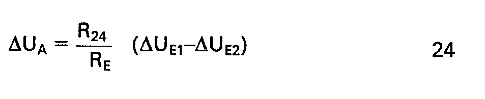
- the output voltage U A is, in a first approximation, only dependent on the current source 30 and the collector resistor 24 of transistor 13:
- the gain v with phase control is under the above conditions and is therefore only dependent on the ratio of the resistors R 24 and R 20 , R 21 , but almost independent of temperature fluctuations AT and supply voltage fluctuations ⁇ Uv.
- a circuit for positive voltage supply with transistors of the other conductivity type has the same properties.
- the two input transistors 10 and 11 are of the NPN type and the transistors 12 and 13 of the PNP type.
- line 50 carries positive potential.
- Equations 2 through 9 inserted in equation 1 gives:
- Equation 10 solved for U A gives:
- the symmetrical design of the amplifier compensates for the effects of temperature on the base-emitter voltage.
- the base-emitter voltage U BE is dependent on the collector current I c and thus on the input voltage U E1 and U E2 .
- transistor 10 at room temperature The following applies to transistor 10 at room temperature:
- equation 17 can be transformed into:
- Equation 11 inserted in Equation 22 gives:
- the gain thus depends advantageously only on the ratio of two resistors.
Landscapes
- Engineering & Computer Science (AREA)
- Power Engineering (AREA)
- Amplifiers (AREA)
Description
- Die Erfindung bezieht sich auf einen wie im Oberbegriff des Patentanspruches 1 angegebenen Verstärker mit gleichspannungsgekoppelten Transistoren.
- Ein derartiger Verstärker ist bereits aus der DE-A-26 33 952 bekannt. Bei dem bekannten Verstärker sind die beiden Transistorstufen als Kollektorschaltung ohne Gegenkopplung geschaltet. In den Emitterzuführungen sind hochohmige Belastungen angeordnet, um eine hohe Verstärkung zu erzielen. Eine hohe Verstärkung ergibt sich auch dadurch, dass eine an die Differenzeingänge angelegte Differenzspannung voll an der Basis-Emitter-Strecke des weiteren Transistors wirksam wird. Der Differenzverstärker ist für einen Aufbau als integrierte Schaltung und eine Verwendung als Operationsverstärker vorgesehen. Im Hinblick auf die sich ergebenden Phasendrehungen wird ein Phasenkompensationskondensator empfohlen.
- Ferner ist aus der Zeitschrift NTZ, Jahrgang 19, Heft 2, Februar 1966, Seiten 65 bis 69 ein Operationsverstärker bekannt, der über äussere Schaltelemente stark gegengekoppelt wird, so dass sich die gewünschte Verstärkung und eine grosse Gleichtaktunterdrückung, in einem gewissen Bereich, weitgehend unabhängig von Versorgungsspannungs- und Temperaturschwankungen einstellt. Hierbei ist die Verstärkung als Quotient der Spannung an den Ausgangsklemmen und der Spannungsdifferenz an den Eingangsklemmen definiert.
- Aufgabe der Erfindung ist es, einen Verstärker mit gleichspannungsgekoppelten Transistorstufen mit einem Differenzeingang und mit einem unsymmetrischen Ausgang derart auszubilden, dass er eine definierte Verstärkung hat und bei geringem Bauteileaufwand und kleinem Versorgungsstrom ein gutes Hochfrequenzverhalten aufweist. Insbesondere soll der Verstärker zur Verwendung in Phasenregelkreisen geeignet sein, bei denen besonders hohe Anforderungen an die Regelsteilheit gestellt werden.
- Ein Phasenregelkreis, bei dem der die Frequenz des Oszillators steuernde Verstärker einen Differenzeingang und einen unsymmetrischen Ausgang erfordert, geht aus E. Stadler: «Modulationsverfahren», Vogel-Verlag, 2. Auf)., 1980, Seiten 60 bis 62 hervor.
- Gemäss der Erfindung wird der Verstärker zur Lösung der gestellten Aufgabe in der im kennzeichnenden Teil des Patentanspruches 1 angegebenen Weise ausgebildet. Dabei ist die Diode für den Konstantstrom in Durchlassrichtung gepolt.
- Durch diese Massnahmen ergibt sich der Vorteil, dass sich bei definierter Verstärkung eine grosse Gleichtaktunterdrückung und ein günstiges Hochfrequenzverhalten bei kleiner Stromaufnahme und geringem Bauteileaufwand miteinander vereinigen lassen. Ausserdem lässt sich die mittlere Ausgangsgleichspannung unabhängig von der Verstärkung wählen.
- Als Diode kann eine Halbleiterdiode mit geeigneter Kennlinie dienen. In Weiterbildung der Erfindung ergibt sich eine besonders weitgehende Temperaturkompensation der Ausgangsspannung dadurch, dass die Diode durch einen Transistor gebildet ist, bei dem die Basis und der Kollektor miteinander verbunden sind.
- Als Transistoren, die Einzeltransistoren sein können, finden vorzugsweise solche mit grosser Stromverstärkung B und hoher Transitfrequenz bei kleinem Kollektorstrom Verwendung.
- Eine besonders weitgehende Verringerung der Temperaturabhängigkeit und der Auswirkung von Exemplarstreuungen auf die Ausgangsspannung lässt sich dadurch erzielen, dass die Transistoren der Emitterstufen durch einen monolithisch aufgebauten Doppeltransistor gebildet sind und/oder dass der weitere, mit dem Ausgang verbundene Transistor und der die Diode bildende Transistor durch einen Monolithisch ausgebildeten Doppeltransistor gebildet sind. Dabei ergibt sich eine besonders weitgehende Gleichtaktunterdrückung.
- Die genannten vorteilhaften Eigenschaften machen den Verstärker besonders geeignet für die im Patentanspruch 5 angegebene Verwendung in einem Phasenregelkreis. Dabei lässt sich eine definierte Vergrösserung der Regelsteilheit des Phasenregelkreises erzielen, was insbesondere bei einem Phasenregelkreis in einer Taktrückgewinnungsschaltung für PCM-Regeneratoren von besonderem Vorteil sein kann. Dabei wird der dem Phasenvergleicher folgende Tiefpass durch den hohen Eingangswiderstand des Verstärkers in vorteilhafter Weise nur wenig belastet.
- Die Erfindung wird anhand der in den Figuren dargestellten Ausführungsbeispiele näher erläutert.
- Es zeigen
- Fig. 1 einen Verstärker mit Differenzeingang und unsymmetrischem Ausgang und
- Fig. 2 einen mit Strom- und Spannungspfeilen versehenen Stromlauf des Verstärkers nach Fig. 1
- Fig. 1 zeigt einen Verstärker für eine negative Spannungsversorgung gegenüber Masse. Die Schaltung enthält zwei PNP-Eingangstransistoren, einen Transistor 10 mit nichtinvertierendem Eingang 1 sowie einen Transistor 11 mit invertierendem Eingang 2. Die Emitter dieser Transistoren 10, 11 sind über die Widerstände 20, 21 an die Massepotential-Leitung 40 gelegt, die ihrerseits auf Masse G liegt. Die Kollektoren dieser Transistoren 10, 11 sind jeweils mit den Emittern von zwei NPN-Transistoren 12 bzw. 13 verbunden und liegen über die Widerstände 22 bzw. 23 an der gegenüber Masse negativen Leitung 50 der Stromversorgung.
- Die Basisanschlüsse der Transistoren 12, 13 sowie der Kollektoranschluss von Transistor 12 sind miteinander verbunden und liegen über eine Konstantstromquelle 30 an der Massepotential-Leitung 40. Der Kollektor von Transistor 13 ist über den Lastwiderstand 24, an dem das Ausgangssignal abgenommen werden kann, ebenfalls mit der Massepotential-Leitung 40 verbunden. Der Transistor 12 ist dabei als Diode geschaltet. Das Ausgangssignal liegt zwischen dem Ausgangsanschluss 3 und Masse.
- Die Widerstände 22 und 23 werden zweckmässigerweise im Hinblick auf eine hohe Grenzfrequenz so gross wie möglich und so klein, wie es mit Rücksicht auf den bei gegebener Versorgungsspannung erforderlichen Spannungshub am Ausgang nötig ist, bemessen.
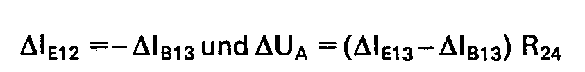
- Fig. 2 zeigt den Stromlauf mit Strom- und Spannungspfeilen. Die Funktionsweise des Verstärkers beruht darauf, dass die Höhe der Spannungen an den Widerständen 22 und 23 bis auf minimale Unterschiede (Einfluss des Kollektor-Stromes lC13 auf die Basis-Emitter-Spannung UBE13 von Transistor 13) übereinstimmen. Das bedeutet, dass die Summe der Einzelströme durch die Widerstände 22,23 mit guter Näherung gleich gross sind (lC10 + lE12 = lC11 + lE13). wenn die Widerstände 20 und 21 bzw. 22 und 23 den gleichen Widerstandwert haben (R20 = R21 = RE und R22 = R23 = Rc).
- Die Transistoren 10 und 11 bzw. 12 und 13 haben zweckmässigerweise die gleichen monolithisch aufgebaute Doppeltransistoren mit üblichen Stromverstärkungen. In diesem Fall gilt B10 = B11 = B12 = B13 = B und β10 = β11 - β12 = β13 = β. Die Basis-Emitter-Spannungen sind gleich gross (UBE10 = BBE11 = UBE12 = UBE13) und die Basis-Emitter-Spannungsänderungen auf Grund von Kollektor Stromänderungen sind vernachlässigbar gegenüber den wirksamen Steuerspannungsänderungen der Transistoren (△UBE10 = △UBE11 = △UBE12 = △UBE13 = 0).
- Die Stromquelle 30 ist ein Zweipol, der als Konstantstromschaltung ausgebildet ist. Derartige Zweipole sind als solche bekannt, z.B. als sogenannte Konstantstromdioden, die aus einem Feldeffekttransistor mit Widerstand bestehen. Derartige Stromquellen sind für den vorliegenden Fall praktisch als ideal zu betrachten, d.h. der Strom l30 ist praktisch konstant.
- Findet keine Aussteuerung des Verstärkers statt, d.h. beide Eingangspegel sind gleich hoch △UE1 = △UE2 = 0, UE1 = UE2) SO ist lC10 = lC11 und IE13 =IE12.
Da UA =lC13. R24,lE12 =l30―lB13 und
- Bei den üblichen Gleichstromverstärkungen ist die Ausgangsspannung UA in erster Näherung nur abhängig von der Stromquelle 30 und dem Kollektorwiderstand 24 von Transistor 13:

- Findet eine Aussteuerung des Verstärkers statt, d.h. ändern sich die Kollektorströme lC10 und lC11 der Eingangstransistoren 10, 11 gegenphasig auf Grund von gegenphasiger Ansteuerung der Eingänge (△UE1 =― △UE2), so ändert sich der Emitterstrom des Transistors 13 wie folgt:
- lE13 + △lE13 = lC10 + (△lC10 ― (lC11 + △lC11) + lE12 + △IE12 IE13 = IC10 ― IC11 + IE12 eingesetzt ergibt: △lE13 =△lC10―△lC11 +△lE12wobei

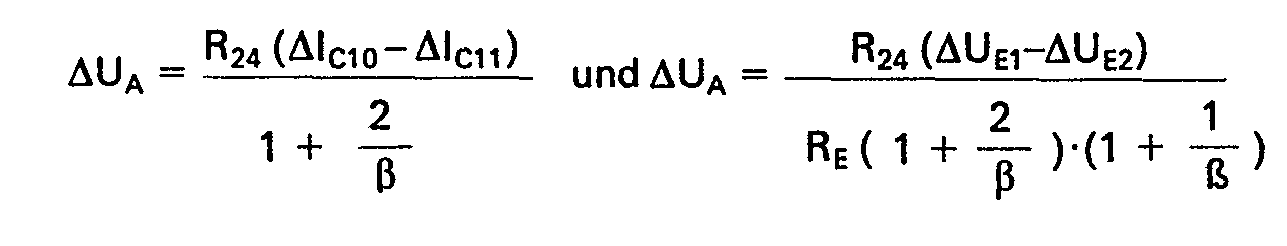
- Durch die symmetrische Anordnung der Eingangstransistoren 10, 11 in der Schaltung, werden Einflüsse von Gleichtakt-Eingangs-Spannungsänderung (△UE1 = △UE2) und Einflüsse von gleichartigen Parameteränderungen der entsprechenden Transistoren auf die Ausgangsspannung unterdrückt. Ebenfalls haben Spannungsänderungen der Basis-Emitter-Strecken auf Grund von Temperatureinflüssen AT an den Transistoren 10, 11, 12, 13 durch den symmetrischen Aufbau der Schaltung keinen Einfluss auf die Ausgangsspannung UA. Zusätzlich ist die Ausgangsspannung UA in weiten Grenzen unabhängig von Versorgungsspannungs-Schwankungen △UV.
- Die Verstärkung v bei gegenphasiger Aussteuerung beträgt unter den genannten Voraussetzungen

- Der Eingangswiderstand REin der Schaltung kann in etwa mit REin = h11E + h21E · RE angegeben werden. Da h11E < < h21E . RE ist, so ist REin ≈ RE. β und damit sehr hochohmig.
- Die gleichen Eigenschaften hat eine Schaltung für positive Spannungsversorgung mit Transistoren des anderen Leitungstyps. In diesem Fall sind die beiden Eingangstransistoren 10 und 11 vom Typ NPN und die Transistoren 12 und 13 vom Typ PNP. Die Leitung 50 führt in diesem Fall positives Potential.
- Anhang: Allgemeine Ableitung der Formeln.
- Nach Fig. 2 können folgende Gleichungen aufgestellt werden:


-

-

- Der weiteren Betrachtung wird die folgende Bemessung zugrunde gelegt:
- UE1 = UE2, R20 = R21 = RE, R22 = R23 = RC, B10=B11=B.B > > 1; β > >1
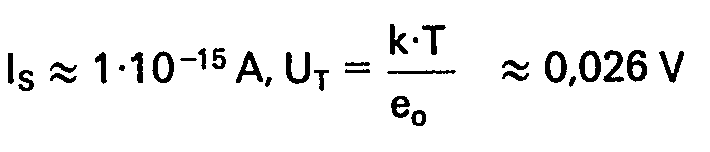
- Ferner ist UBE = UT 1 n (

- Ferner ändert sich die Basis-Emitter-Spannung bei konstantem Basisstrom sehr wenig mit der Kollektor-Emitter-Spannung.
- △UBE ≈ 10―5 .△UCE IB = konst. und damit ist auch UBe12 ≈ UBE13
- Weiterhin ändert sich die Basis-Emitter-Spannung der Transistoren mit der Temperatur.

- Durch den symmetrischen Aufbau des Verstärkers kompensieren sich die Einflüsse der Temperatur auf die Basis-Emitter-Spannung.
- 1. Wird der Verstärker nicht ausgesteuert, so gilt: △UE1 = △UE2
- Aus Gleichung 11 wird dann


- 2. Wird der Verstärker ausgesteuert, so gilt:


- Bei den Eingangstransistoren 10, 11 ist die Basis-Emitter-Spannung UBE abhängig von dem Kollektorstrom Ic und damit von der Eingangsspannung UE1 bzw. UE2.
- Für den Transistor 10 gilt bei Raumtemperatur:

- Bei Raumtemperatur gilt:


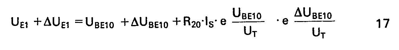


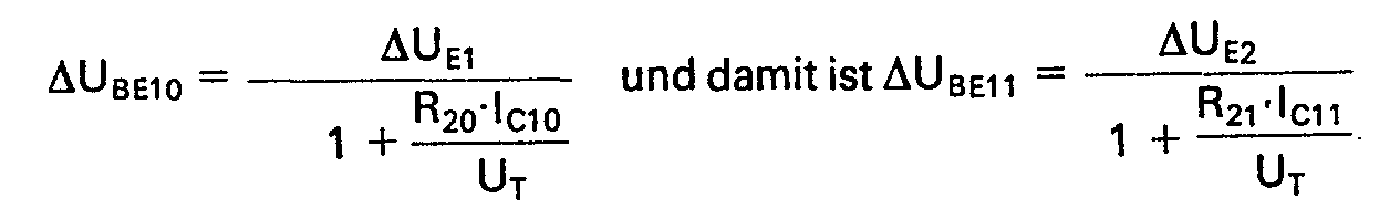
- Auch bei kleinen Kollektorströmen lC10 bzw. lC11 ist △UBE10 < < △UE1 bzw. △UBE11 < < △UE2 und daher vernachlässigbar in ihrem Einfluss auf die Steuerspannung der beiden Steuertransistoren, wenn die Widerstandsverhältnisse


und daher vernachlässigbar. - Es ist △UBE12 < < △UBE13 da △lC12 < < △lC13 und damit kann die Gleichung 11 erweitert werden:


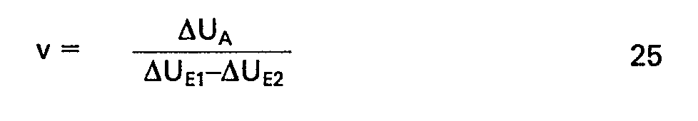

- Die Verstärkung hängt somit in vorteilhafter Weise nur vom Verhältnis zweier Widerstände ab.
Claims (5)
geführt ist und dass die Ausgangselektrode des Transistors (11) der einen Emitterstufe, mit der der Emitter des weiteren Transistors (13) verbunden ist, der Kollektor des Transistors (11) ist und dass die Diode (12), mit der die Basis des weiteren Transistors (13) verbunden ist, an den Kollektor des Transistors (10) der anderen Emitterstufe geführt ist.
Priority Applications (1)
| Application Number | Priority Date | Filing Date | Title |
|---|---|---|---|
| AT83109276T ATE24804T1 (de) | 1982-09-21 | 1983-09-19 | Verstaerker mit gleichspannungsgekoppelten transistorstufen. |
Applications Claiming Priority (2)
| Application Number | Priority Date | Filing Date | Title |
|---|---|---|---|
| DE3234901A DE3234901C2 (de) | 1982-09-21 | 1982-09-21 | Verstärker mit gleichspannungsgekoppelten Transistorstufen |
| DE3234901 | 1982-09-21 |
Publications (2)
| Publication Number | Publication Date |
|---|---|
| EP0106190A1 EP0106190A1 (de) | 1984-04-25 |
| EP0106190B1 true EP0106190B1 (de) | 1987-01-07 |
Family
ID=6173750
Family Applications (1)
| Application Number | Title | Priority Date | Filing Date |
|---|---|---|---|
| EP83109276A Expired EP0106190B1 (de) | 1982-09-21 | 1983-09-19 | Verstärker mit gleichspannungsgekoppelten Transistorstufen |
Country Status (3)
| Country | Link |
|---|---|
| EP (1) | EP0106190B1 (de) |
| AT (1) | ATE24804T1 (de) |
| DE (2) | DE3234901C2 (de) |
Families Citing this family (1)
| Publication number | Priority date | Publication date | Assignee | Title |
|---|---|---|---|---|
| GB2312579A (en) * | 1996-04-25 | 1997-10-29 | Plessey Semiconductors Ltd | A differential amplifier with I/P buffer differential amplifiers including current mirrors |
Family Cites Families (3)
| Publication number | Priority date | Publication date | Assignee | Title |
|---|---|---|---|---|
| BE755452A (fr) * | 1969-08-29 | 1971-03-01 | Siemens Ag | Montage pour un amplificateur differentiel en circuit integre |
| US3894290A (en) * | 1973-06-15 | 1975-07-08 | Motorola Inc | Balanced double-to-single-ended converter stage for use with a differential amplifier |
| JPS5216950A (en) * | 1975-07-30 | 1977-02-08 | Hitachi Ltd | Differential amplification circuit |
-
1982
- 1982-09-21 DE DE3234901A patent/DE3234901C2/de not_active Expired
-
1983
- 1983-09-19 AT AT83109276T patent/ATE24804T1/de not_active IP Right Cessation
- 1983-09-19 EP EP83109276A patent/EP0106190B1/de not_active Expired
- 1983-09-19 DE DE8383109276T patent/DE3369040D1/de not_active Expired
Also Published As
| Publication number | Publication date |
|---|---|
| DE3234901A1 (de) | 1984-03-22 |
| DE3369040D1 (en) | 1987-02-12 |
| EP0106190A1 (de) | 1984-04-25 |
| ATE24804T1 (de) | 1987-01-15 |
| DE3234901C2 (de) | 1984-09-06 |
Similar Documents
| Publication | Publication Date | Title |
|---|---|---|
| DE69933160T2 (de) | Hochfrequenzverstärker | |
| DE69003385T2 (de) | Logarithmischer verstärker. | |
| DE1906213B2 (de) | Stromregelschaltung | |
| DE69321902T2 (de) | Umsetzerschaltung und Doppelgegentaktmischer | |
| US4327319A (en) | Active power supply ripple filter | |
| DE2424812B2 (de) | Verstärker mit Überstromschutz | |
| DE2513906B2 (de) | Stromspiegelverstaerker | |
| DE69718301T2 (de) | Linearer hochfrequenzverstärker mit hoher eingangsimpedanz und hohem leistungswirkungsgrad | |
| DE1901804B2 (de) | Stabilisierter differentialverstaerker | |
| US4567444A (en) | Current mirror circuit with control means for establishing an input-output current ratio | |
| DE3686431T2 (de) | Schaltung zur detektion eines automatischen verstaerkungsregelungssignals. | |
| DE3035272A1 (de) | Operations-transkonduktanzverstaerker mit einer nichtlineare komponente aufweisenden stromverstaerkern | |
| DE2836914A1 (de) | Optisch gekoppelte vorspannungsschaltung fuer eine komplementaere ausgangsschaltung | |
| DE4009614A1 (de) | Schaltung mit automatischer verstaerkungsregelung | |
| DE2533421A1 (de) | Monolithischer verstaerker | |
| DE2540867C2 (de) | Temperaturkompensierte emittergekoppelte Multivibratorschaltung | |
| DE4307606A1 (de) | Leistungsverstärker | |
| DE2438255A1 (de) | Stromverstaerker | |
| DE69002344T2 (de) | Spannungskontrollierter emittergekoppelter Multivibrator mit zwei Eingängen. | |
| EP0106190B1 (de) | Verstärker mit gleichspannungsgekoppelten Transistorstufen | |
| DE2445738A1 (de) | Leistungsverstaerker | |
| DE3824105C2 (de) | Schaltungsanordnung zum Erzeugen einer stabilisierten Ausgangsspannung | |
| JP3081210B2 (ja) | 線形利得増幅回路 | |
| DE2445134B2 (de) | Verstärkerschaltung | |
| DE3007715A1 (de) | Verstaerkerschaltung mit durch eine steuerspannung steuerbarer gesamtverstaerkung |
Legal Events
| Date | Code | Title | Description |
|---|---|---|---|
| PUAI | Public reference made under article 153(3) epc to a published international application that has entered the european phase |
Free format text: ORIGINAL CODE: 0009012 |
|
| AK | Designated contracting states |
Designated state(s): AT BE CH DE FR GB IT LI NL SE |
|
| 17P | Request for examination filed |
Effective date: 19840524 |
|
| GRAA | (expected) grant |
Free format text: ORIGINAL CODE: 0009210 |
|
| AK | Designated contracting states |
Kind code of ref document: B1 Designated state(s): AT BE CH DE FR GB IT LI NL SE |
|
| PG25 | Lapsed in a contracting state [announced via postgrant information from national office to epo] |
Ref country code: NL Effective date: 19870107 |
|
| REF | Corresponds to: |
Ref document number: 24804 Country of ref document: AT Date of ref document: 19870115 Kind code of ref document: T |
|
| PG25 | Lapsed in a contracting state [announced via postgrant information from national office to epo] |
Ref country code: SE Effective date: 19870131 |
|
| REF | Corresponds to: |
Ref document number: 3369040 Country of ref document: DE Date of ref document: 19870212 |
|
| ET | Fr: translation filed | ||
| ITF | It: translation for a ep patent filed | ||
| NLV1 | Nl: lapsed or annulled due to failure to fulfill the requirements of art. 29p and 29m of the patents act | ||
| PLBE | No opposition filed within time limit |
Free format text: ORIGINAL CODE: 0009261 |
|
| STAA | Information on the status of an ep patent application or granted ep patent |
Free format text: STATUS: NO OPPOSITION FILED WITHIN TIME LIMIT |
|
| 26N | No opposition filed | ||
| PG25 | Lapsed in a contracting state [announced via postgrant information from national office to epo] |
Ref country code: GB Effective date: 19890919 Ref country code: AT Effective date: 19890919 |
|
| PG25 | Lapsed in a contracting state [announced via postgrant information from national office to epo] |
Ref country code: LI Effective date: 19890930 Ref country code: CH Effective date: 19890930 Ref country code: BE Effective date: 19890930 |
|
| BERE | Be: lapsed |
Owner name: SIEMENS A.G. BERLIN UND MUNCHEN Effective date: 19890930 |
|
| GBPC | Gb: european patent ceased through non-payment of renewal fee | ||
| REG | Reference to a national code |
Ref country code: CH Ref legal event code: PL |
|
| PGFP | Annual fee paid to national office [announced via postgrant information from national office to epo] |
Ref country code: FR Payment date: 19910917 Year of fee payment: 9 |
|
| ITTA | It: last paid annual fee | ||
| PG25 | Lapsed in a contracting state [announced via postgrant information from national office to epo] |
Ref country code: FR Effective date: 19930528 |
|
| REG | Reference to a national code |
Ref country code: FR Ref legal event code: ST |
|
| PGFP | Annual fee paid to national office [announced via postgrant information from national office to epo] |
Ref country code: DE Payment date: 19951116 Year of fee payment: 13 |
|
| PG25 | Lapsed in a contracting state [announced via postgrant information from national office to epo] |
Ref country code: DE Effective date: 19970603 |