EP0106201B1 - Anzeigesteuereinrichtung zum Lesen von Anzeigedaten aus einem dynamischen Video-RAM und gleichzeitigen Auffrischen von Speicherzellen des Video-RAMS - Google Patents
Anzeigesteuereinrichtung zum Lesen von Anzeigedaten aus einem dynamischen Video-RAM und gleichzeitigen Auffrischen von Speicherzellen des Video-RAMS Download PDFInfo
- Publication number
- EP0106201B1 EP0106201B1 EP83109349A EP83109349A EP0106201B1 EP 0106201 B1 EP0106201 B1 EP 0106201B1 EP 83109349 A EP83109349 A EP 83109349A EP 83109349 A EP83109349 A EP 83109349A EP 0106201 B1 EP0106201 B1 EP 0106201B1
- Authority
- EP
- European Patent Office
- Prior art keywords
- address
- row
- video ram
- raster
- bits
- Prior art date
- Legal status (The legal status is an assumption and is not a legal conclusion. Google has not performed a legal analysis and makes no representation as to the accuracy of the status listed.)
- Expired
Links
Images



Classifications
-
- G—PHYSICS
- G09—EDUCATION; CRYPTOGRAPHY; DISPLAY; ADVERTISING; SEALS
- G09G—ARRANGEMENTS OR CIRCUITS FOR CONTROL OF INDICATING DEVICES USING STATIC MEANS TO PRESENT VARIABLE INFORMATION
- G09G5/00—Control arrangements or circuits for visual indicators common to cathode-ray tube indicators and other visual indicators
- G09G5/22—Control arrangements or circuits for visual indicators common to cathode-ray tube indicators and other visual indicators characterised by the display of characters or indicia using display control signals derived from coded signals representing the characters or indicia, e.g. with a character-code memory
- G09G5/222—Control of the character-code memory
Definitions
- This invention relates to a display control circuit which effectively refreshes memory cells of a video RAM constituted by a dynamic RAM.
- a CRT control device includes a video RAM. If the video RAM is a dynamic RAM, it is necessary to repeatedly refresh the RAM at predetermined intervals of 2 msec or less. Otherwise, the data stored in the memory cells would be lost.
- the memory cells of the dynamic RAM are usually arranged in a matrix form. To read data from, or write it into, one memory cell, a row address and a column address are supplied to the RAM chip. The row address designate the memory cells of one row. Items of data are read from these memory cells and stored into a buffer amplifier (refresh amplifier) provided within the RAM chip. The items of data stored in the buffer amplifier are written back into the memory cells of the row. Therefore, these memory cells are- refreshed every time a row address is supplied to the dynamic RAM. In the case of 4K bits dynamic RAM having a memory cell matrix of 64 bitsx64 bits, all memory cells are refressed when all the 64 row addresses are accessed.
- the reading of display data from the-video RAM is synchronized with the display of the data by the CRT display unit. If the items of data to be displayed are stored in a column of memory cells in the order of reading, the cells can be refreshed when the items of data are read to be displayed.
- a method of arranging bits forming a character code in the column of memory cells is described in Japanese Patent Discosure No. 79-731.
- This method is effective only for the certain format of the CRT screen in which the number of characters (digits) per display row is relatively large (e.g., 64 or 80 digits) and the number of rasters per display row is relatively small (e.g., 8 or 10 rasters).
- the CRT screen has 64 digits per row and 10 rasters per row, a time period for displaying one row is 640 Il sec if a display period for one raster is 64 ⁇ sec. Therefore, three rows can be displayed in 2 msec.
- the video RAM is a dynamic RAM of 16 Kb (128-bitsx128-bits)
- all memory cells can be refreshed within one refresh cycle of 2 msec.
- the prior art method has the following drawbacks.
- the screen has 40 digits per row and 20 rasters per row, the period for displaying one row is 1.28 msec. Therefore, only 80 row addresses are accessed within 2.56 msec.
- a display control circuit comprising a video RAM for storing data to be displayed on a display screen each row of which is constituted by several rasters, a read controller for producing a raster address and memory address to read the data from the video RAM, and a circuit for supplying a row address and a column address which are obtained from the raster address amd memory address produced by the read controller so that the raster address is included in the row address supplied to the video RAM.
- Fig. 1 shows a block diagram of a computer system mainly based on the display control circuit 10 of a first embodiment.
- the circuit 10 is connected to a central processor unit (CPU) 14 through a system bus 12.
- CPU 14 controls the whole system.
- the system bus 12 is comprised of an address bus AD, a control bus CTRL and a data bus DATA.
- the display control circuit 10 synchronizes a video RAM (VRAM) 16 and its peripheral circuit with a CRT display unit (not shown).
- VRAM 16 stores 2048 characters represented by ANK character codes. Since an ANK code is an 8-bit code, it is sufficient for VRAM 16 to have a 2Kb-capacity.
- a writing address CPU ADR is supplied from CPU 14 to a first input terminal of an address selector 18.
- CPU ADR accesses the VRAM 16 of 4Kb so that the bit length of CPU ADR is 14 bits.
- a raster address RA and a refresh memory address MA are generated from a CRT controller (CRTC) 20 to output display data from the VRAM 16 to the CRT display unit.
- CRTC 20 further generates a horizontal synchronizing signal HSYNC and a vertical synchronizing signal VSYNC.
- the memory address MA is a memory address signal for refreshing a video frame displayed on the CRT display unit for a predetermined period.
- the memory address MA is 11 bits long.
- the raster address RA is supplied to a character generator 22 and used as a raster selection signal.
- the memory address MA and the least significant bit of the raster address RA are supplied to a second input terminal of the address selector 18.
- a timing & wait controller 24 produces a character clock (CLK) determining the timing of the RA, MA, HSYNC and VSYNC and supplies it to CRTC 20.
- CLK character clock
- the timing & wait controller 24 supplies and address selection signal SEL and a column selection signal COL to the address selector 18.
- One of the CPU ADR and MA is selected by the address selection signal SEL.
- the output signal from. the address selector 18 is divided into a row address and a column address according to the column section signal COL and the divided one is supplied to VRAM 16.
- the timing & wait controller 24 supplies a row address selection signal (RAS) and a column address selection signal TC-A-9) to VRAM 16.
- the video RAM 16 decodes the row address in response to the RAS and decodes the column address in response to the CAS.
- VRAM 16 includes a row address decoder and a column address decoder.
- the character code read from VRAM 16 to be displayed is supplied to the character generator 22.
- the character generator 22- produces pattern data of one raster corresponding to the character code and raster address RA. This pattern data is supplied to a shift register 26 and converted to a serial dot signal VID.
- the VRAM 16 is accessed by the CPU 16 when an access request is supplied to the timing & wait controller 24 through the CRT controller 20. If the video RAM access achieved by CRTC 29 comes into collision with the video RAM access achieved by CPU 14, the timing & wait controller 24 sets CPU 14 in waiting mode. When the waiting mode ends, CPU 14 produces the CPU ADR through the address bus AD. When the character codes are written into the VRAM 16, the data are stored into a data buffer 28. At this time, the timing & wait controller 24 produces an address selection signal SEL, which causes the address selector 18 to select the CPU ADR.
- SEL address selection signal
- the memory address and the bit 0 of the raster address RA MA are combined to form a video RAM access address, with the RA being used as the least significant bit. Therefore, the video RAM access address for display is a 12-bit address.
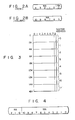
- the upper six bits of the access address and the lower six bits of the access address are supplied to the VRAM 16 as the row address and the column address respectively, as shown in Figs. 2A and 2B.
- VRAM 16 for displaying 2048 characters on the CRT display unit has a 2Kb-capacity.
- the CRTC 20 supplies only the 11-bit memory address MA to VRAM 16.
- the lower six bits of the memory address MA and the upper five bits of the memory address MA are supplied to VRAM 16 as the row address and the column address.
- 64 digits are displayed in one row, the whole memory cells are refreshed within 1- row display period.
- 32 digits are displayed in one row, the whole memory cells are refreshed in 2-row display period. Therefore, if the number of rasters per row increases, the whole memory cells can not be refreshed within a predetermined period of time.
- the bit 0 of the raster address RA is included in the row address.
- 64 row addresses are accessed within 2-raster period. Therefore, even when 32 digits are displayed in one row, 64 row addresses are refreshed within 2-raster period. Moreover, the refresh cycle is not prolonged with increase of the number of rasters per row.
- the same character code must be stored in the succeeding two addresses of VRAM 16. This is because that the same character code must be read from VRAM 16 when the bit 0 of the RA is "1" and when the bit 0 of the RA is "0".
- the addressing space of VRAM 16 must be increase and the same character code must be written into the increase space. Nevertheless, the embodiment has the advantage that the refresh cycle of the video RAM is greatly shortened.
- bit of raster address RA assigned to the row address and assigne bit of the raster address is not limited to the example described above.
- Fig. 3 is an apparently address map of the video RAM according to the second embodiment.
- the address for the cell matrix is called a physical address.
- the apparently address is called a logic address to distinguish from the physical address.
- One word of the video RAM 16 is of 9 bits.
- the bit 8 of the word is a control bit for indicating that the remaining eight bits form a pattern data or a character code.
- the capacity of the video RAM 16 is 16 KW (words) and distributed in 2 KW units according to the raster address.
- the video RAM 16 comprised of 9 dynamic RAM chips each of 16 Kb (128 bitsx128 bits). When the character codes are written into the video RAM, they are written into the respective 2 KW areas of the video RAM.
- the logical address must have the format shown in Fig. 4 to realize the logical address map as shown in Fig. 3.
- the 3-bit raster address RA is assigned to the upper three bits of the logical address and the 11-bit memory address MA is asssigned to the lower 11 bits of the logical address.
- bit 0(LSB) to bit 6 of the logical address are supplied to VRAM 10 as the row address and the bit 7 to bit 14 of the logical address (i.e., the bit 7 to bit 10 of the memory address MA and the bit 0 to bit 2 of the raster address RA) are supplied as the column address, the following drawback will occur. Since the eight rasters constitute one display row, the time period necessary to display one row is 512 (64x8) H sec. Almost 4 rows are displayed in 2 msec. The number of physical addresses accessed within 2 msec is 4 times the number of digits per row. The complement of the refresh means that 128 row addresses are accessed in 2 msec. It is therefore sufficient that the number of digits per row is not less than 32. If the number of digits per row is less than 32, there will be no margin of the refresh cycle and it is not possible to refresh the memory cells.
- the bits constituting the words defined by the address map shown in Fig. 3 are separately stored in the memory cell matrix of the RAM chip. That is, the row address and the column address (physical address) supplied to the RAM chip are obtained by rearranging the bit location of the logical address shown in Fig. 4.
- Fig. 5 is a block diagram of a computer system mainly based on the display control circuit according to the second embodiment.
- the same reference numerals as used in Fig. 1 will be used in Fig. 5 to denote corresponding portions.
- the second embodiment is a modification of first embodiment, which further comprises an address converter (CONV) 30, a data selector 32 and a signal line 34.
- the video RAM 16 stores the dot pattern data and the character code in a mixed form.
- the data selector 32 selects one of the data MD from the video RAM 16 and the character pattern data CP from the character generator 22 and the selected one is supplied to the shift register 26.
- the selection of the data controller 32 is controlled by the bit 8 (the control bit) of the word in VRAM 16 through the signal line 34.
- the output timings of the data MD and CP are different from each other, so it is necessary to correct the timings of the data MD and CP. However, the timing correction has no direct relevancy to this invention. The description thereof is omitted.
- the address converter 30 is described as a bit-per- mutating means of the memory address MA and the raster address RA. The address converter 30 is realized by changing the connections between the MA, RA output terminals of the CRT controller 20 and the input terminals of the address selector 18.
- the row address and the column address which are produced from the address selector 18 for accessing VRAM 16 to display have the bit-arrangements as shown in Figs. 6A and 6B, respectively.
- the bits 0 and 1 of the raster address RA and the bits 0 to 4 of the memory address MA are assigned to the row address.
- the bit 2 of the raster address RA and the bits 5 to 10 of the memory address MA are assigned to the column address.
- the row address and the column address are alternatively supplied to VRAM 16 according to the column selection signal COL.
- the row address selection signal RAS, the column selection signal COL, the column address selection CAS and the VRAM access address (physical address) are shown by the timing charts of Figs. 7A, 7B, 7C and 7D.
- the raster address RA included in the row address in changed for each raster.
- the memory cells of 16 Kb are all refreshed in that period. If the number of rasters per row and the number of bits of the raster address RA increase, the number of bits of the memory address MA will decrease.
- the row address shown in Fig. 6A can be formed when one row has 32 or more digits and the refresh completes in 256 ⁇ sec.
- the physical address used to conduct the reading operation for refreshing of the video RAM i.e., row addresses
- the physical address used to conduct the reading operation for refreshing of the video RAM is formed of a lower bit portion of the raster address and a lower bit portion of the memory address, whereby the refreshing of the VRAM, as a whole, is completed in a smaller number of raster cycles.
- the refreshing is possible, even when the construction of the display screen is disadvantageous for the refreshing operation, namely, even when the number of rasters per row increases.
- 2 bits of the raster address are assigned to the row address.
- the number of raster addresses assigned to the row address is not limited to two, 3 or more bits may be allotted to the row address.
- the writing of data into the VRAM 16 occurs as follows.
- CPU 14 supplies a memory request signal to the timing & wait controller 24, timing & wait controller 24 may access CPU 14.
- CPU 14 supplies CPU ADR (writing address) to the address selector 18 and the write data to the data buffer 28.
- CPU ADR is a physical address to write data into the VRAM 16.
Landscapes
- Engineering & Computer Science (AREA)
- Physics & Mathematics (AREA)
- Computer Hardware Design (AREA)
- General Physics & Mathematics (AREA)
- Theoretical Computer Science (AREA)
- Controls And Circuits For Display Device (AREA)
- Image Generation (AREA)
Claims (3)
Applications Claiming Priority (2)
| Application Number | Priority Date | Filing Date | Title |
|---|---|---|---|
| JP57163424A JPS5954095A (ja) | 1982-09-20 | 1982-09-20 | ビデオramリフレッシュ方式 |
| JP163424/82 | 1982-09-20 |
Publications (3)
| Publication Number | Publication Date |
|---|---|
| EP0106201A2 EP0106201A2 (de) | 1984-04-25 |
| EP0106201A3 EP0106201A3 (en) | 1985-11-21 |
| EP0106201B1 true EP0106201B1 (de) | 1987-12-02 |
Family
ID=15773634
Family Applications (1)
| Application Number | Title | Priority Date | Filing Date |
|---|---|---|---|
| EP83109349A Expired EP0106201B1 (de) | 1982-09-20 | 1983-09-20 | Anzeigesteuereinrichtung zum Lesen von Anzeigedaten aus einem dynamischen Video-RAM und gleichzeitigen Auffrischen von Speicherzellen des Video-RAMS |
Country Status (4)
| Country | Link |
|---|---|
| US (1) | US4737780A (de) |
| EP (1) | EP0106201B1 (de) |
| JP (1) | JPS5954095A (de) |
| DE (1) | DE3374819D1 (de) |
Families Citing this family (12)
| Publication number | Priority date | Publication date | Assignee | Title |
|---|---|---|---|---|
| CN1012301B (zh) * | 1984-10-16 | 1991-04-03 | 三洋电机株式会社 | 显示装置 |
| JPS6251095A (ja) * | 1985-08-29 | 1987-03-05 | Nec Corp | 画像メモリ駆動方式 |
| US4876663A (en) * | 1987-04-23 | 1989-10-24 | Mccord Donald G | Display interface system using buffered VDRAMs and plural shift registers for data rate control between data source and display |
| US5030946A (en) * | 1987-05-20 | 1991-07-09 | Hudson Soft Co., Ltd. | Apparatus for the control of an access to a video memory |
| US4952924A (en) * | 1988-08-23 | 1990-08-28 | Acer Incorporated | Method and apparatus for address conversion in a chinese character generator of a CRTC scan circuit |
| JP3350043B2 (ja) * | 1990-07-27 | 2002-11-25 | 株式会社日立製作所 | 図形処理装置及び図形処理方法 |
| US5309168A (en) * | 1990-10-31 | 1994-05-03 | Yamaha Corporation | Panel display control device |
| GB2250668B (en) * | 1990-11-21 | 1994-07-20 | Apple Computer | Tear-free updates of computer graphical output displays |
| US5229758A (en) * | 1991-09-05 | 1993-07-20 | Acer Incorporated | Display device controller and method |
| US5394172A (en) * | 1993-03-11 | 1995-02-28 | Micron Semiconductor, Inc. | VRAM having isolated array sections for providing write functions that will not affect other array sections |
| JP4964091B2 (ja) * | 2007-10-30 | 2012-06-27 | 川崎マイクロエレクトロニクス株式会社 | メモリアクセス方法およびメモリ制御装置 |
| JP2009169257A (ja) * | 2008-01-18 | 2009-07-30 | Kawasaki Microelectronics Inc | メモリ制御回路および画像処理装置 |
Family Cites Families (12)
| Publication number | Priority date | Publication date | Assignee | Title |
|---|---|---|---|---|
| JPS5297632A (en) * | 1976-02-12 | 1977-08-16 | Hitachi Ltd | Display unit |
| DE2636788C3 (de) * | 1976-08-16 | 1980-01-31 | Siemens Ag, 1000 Berlin Und 8000 Muenchen | Datenspeicher für Datensichtgeräte |
| JPS54731A (en) * | 1977-06-03 | 1979-01-06 | Inoue Japax Res | Power supply for electric machine tool |
| US4430649A (en) * | 1978-07-21 | 1984-02-07 | Radio Shack | Video processing system |
| US4243984A (en) * | 1979-03-08 | 1981-01-06 | Texas Instruments Incorporated | Video display processor |
| JPS55163578A (en) * | 1979-06-05 | 1980-12-19 | Nippon Electric Co | Image control system |
| JPS6036592B2 (ja) * | 1979-06-13 | 1985-08-21 | 株式会社日立製作所 | 文字図形表示装置 |
| JPS5766590A (en) * | 1980-10-13 | 1982-04-22 | Hitachi Ltd | Dynamic memory refreshing circuit |
| JPS57129585A (en) * | 1981-02-04 | 1982-08-11 | Nec Corp | Memory device |
| JPS57165891A (en) * | 1981-04-06 | 1982-10-13 | Matsushita Electric Industrial Co Ltd | Screen display unit |
| US4408200A (en) * | 1981-08-12 | 1983-10-04 | International Business Machines Corporation | Apparatus and method for reading and writing text characters in a graphics display |
| US4482979A (en) * | 1982-02-04 | 1984-11-13 | May George A | Video computing system with automatically refreshed memory |
-
1982
- 1982-09-20 JP JP57163424A patent/JPS5954095A/ja active Pending
-
1983
- 1983-09-16 US US06/533,003 patent/US4737780A/en not_active Expired - Fee Related
- 1983-09-20 DE DE8383109349T patent/DE3374819D1/de not_active Expired
- 1983-09-20 EP EP83109349A patent/EP0106201B1/de not_active Expired
Also Published As
| Publication number | Publication date |
|---|---|
| JPS5954095A (ja) | 1984-03-28 |
| EP0106201A3 (en) | 1985-11-21 |
| DE3374819D1 (en) | 1988-01-14 |
| US4737780A (en) | 1988-04-12 |
| EP0106201A2 (de) | 1984-04-25 |
Similar Documents
| Publication | Publication Date | Title |
|---|---|---|
| US4670752A (en) | Hard-wired circuit for handling screen windows | |
| EP0106201B1 (de) | Anzeigesteuereinrichtung zum Lesen von Anzeigedaten aus einem dynamischen Video-RAM und gleichzeitigen Auffrischen von Speicherzellen des Video-RAMS | |
| US5539428A (en) | Video font cache | |
| US4870491A (en) | Display control apparatus for supplying display data to raster scanning type display device | |
| US4563677A (en) | Digital character display | |
| US4201983A (en) | Addressing circuitry for a vertical scan dot matrix display apparatus | |
| EP0215984B1 (de) | Graphik-Anzeigegerät mit kombiniertem Bitpuffer und Zeichengraphikspeicherung | |
| JP2940809B2 (ja) | ダイナミックランダムアクセスメモリ、ダイナミックランダムアクセスメモリのアクセス方法及びシステム | |
| US4937565A (en) | Character generator-based graphics apparatus | |
| US4417318A (en) | Arrangement for control of the operation of a random access memory in a data processing system | |
| JP2827361B2 (ja) | 半導体メモリ装置 | |
| JP2986716B2 (ja) | オンスクリーンディスプレイのフォントrom制御回路 | |
| EP0283579B1 (de) | Nach dem Rasterverfahren arbeitendes Anzeigesystem mit einem einen Randomspeicher enthaltenden Zeichengenerator | |
| JP2708841B2 (ja) | ビットマップメモリの書き込み方法 | |
| EP0420291B1 (de) | Anzeigesteuergerät | |
| JPS597115B2 (ja) | アドレス作成方法 | |
| JP2846357B2 (ja) | フォントメモリ装置 | |
| JPH09106374A (ja) | 画像メモリ装置 | |
| JPS6228473B2 (de) | ||
| JPS6327713B2 (de) | ||
| JPH0146072B2 (de) | ||
| JPS632117B2 (de) | ||
| JPS5817487A (ja) | 表示制御装置 | |
| JPS6024586A (ja) | 表示デ−タの処理回路 | |
| JPH023513B2 (de) |
Legal Events
| Date | Code | Title | Description |
|---|---|---|---|
| PUAI | Public reference made under article 153(3) epc to a published international application that has entered the european phase |
Free format text: ORIGINAL CODE: 0009012 |
|
| 17P | Request for examination filed |
Effective date: 19831017 |
|
| AK | Designated contracting states |
Designated state(s): DE FR GB IT |
|
| RAP1 | Party data changed (applicant data changed or rights of an application transferred) |
Owner name: KABUSHIKI KAISHA TOSHIBA |
|
| PUAL | Search report despatched |
Free format text: ORIGINAL CODE: 0009013 |
|
| AK | Designated contracting states |
Designated state(s): DE FR GB IT |
|
| 17Q | First examination report despatched |
Effective date: 19870120 |
|
| GRAA | (expected) grant |
Free format text: ORIGINAL CODE: 0009210 |
|
| AK | Designated contracting states |
Kind code of ref document: B1 Designated state(s): DE FR GB IT |
|
| ITF | It: translation for a ep patent filed | ||
| REF | Corresponds to: |
Ref document number: 3374819 Country of ref document: DE Date of ref document: 19880114 |
|
| ET | Fr: translation filed | ||
| PLBE | No opposition filed within time limit |
Free format text: ORIGINAL CODE: 0009261 |
|
| STAA | Information on the status of an ep patent application or granted ep patent |
Free format text: STATUS: NO OPPOSITION FILED WITHIN TIME LIMIT |
|
| 26N | No opposition filed | ||
| ITTA | It: last paid annual fee | ||
| PGFP | Annual fee paid to national office [announced via postgrant information from national office to epo] |
Ref country code: FR Payment date: 19960910 Year of fee payment: 14 |
|
| PGFP | Annual fee paid to national office [announced via postgrant information from national office to epo] |
Ref country code: GB Payment date: 19960911 Year of fee payment: 14 |
|
| PGFP | Annual fee paid to national office [announced via postgrant information from national office to epo] |
Ref country code: DE Payment date: 19960927 Year of fee payment: 14 |
|
| PG25 | Lapsed in a contracting state [announced via postgrant information from national office to epo] |
Ref country code: GB Free format text: LAPSE BECAUSE OF NON-PAYMENT OF DUE FEES Effective date: 19970920 |
|
| PG25 | Lapsed in a contracting state [announced via postgrant information from national office to epo] |
Ref country code: FR Free format text: THE PATENT HAS BEEN ANNULLED BY A DECISION OF A NATIONAL AUTHORITY Effective date: 19970930 |
|
| GBPC | Gb: european patent ceased through non-payment of renewal fee |
Effective date: 19970920 |
|
| PG25 | Lapsed in a contracting state [announced via postgrant information from national office to epo] |
Ref country code: DE Free format text: LAPSE BECAUSE OF NON-PAYMENT OF DUE FEES Effective date: 19980603 |
|
| REG | Reference to a national code |
Ref country code: FR Ref legal event code: ST |