EP0106617A2 - Procédé de fabrication d'un EEPROM - Google Patents
Procédé de fabrication d'un EEPROM Download PDFInfo
- Publication number
- EP0106617A2 EP0106617A2 EP83306004A EP83306004A EP0106617A2 EP 0106617 A2 EP0106617 A2 EP 0106617A2 EP 83306004 A EP83306004 A EP 83306004A EP 83306004 A EP83306004 A EP 83306004A EP 0106617 A2 EP0106617 A2 EP 0106617A2
- Authority
- EP
- European Patent Office
- Prior art keywords
- region
- insulating layer
- tunneling insulating
- gate
- eeprom
- Prior art date
- Legal status (The legal status is an assumption and is not a legal conclusion. Google has not performed a legal analysis and makes no representation as to the accuracy of the status listed.)
- Granted
Links
Images

Classifications
-
- H—ELECTRICITY
- H10—SEMICONDUCTOR DEVICES; ELECTRIC SOLID-STATE DEVICES NOT OTHERWISE PROVIDED FOR
- H10D—INORGANIC ELECTRIC SEMICONDUCTOR DEVICES
- H10D30/00—Field-effect transistors [FET]
- H10D30/01—Manufacture or treatment
- H10D30/021—Manufacture or treatment of FETs having insulated gates [IGFET]
- H10D30/0411—Manufacture or treatment of FETs having insulated gates [IGFET] of FETs having floating gates
-
- H—ELECTRICITY
- H10—SEMICONDUCTOR DEVICES; ELECTRIC SOLID-STATE DEVICES NOT OTHERWISE PROVIDED FOR
- H10D—INORGANIC ELECTRIC SEMICONDUCTOR DEVICES
- H10D30/00—Field-effect transistors [FET]
- H10D30/60—Insulated-gate field-effect transistors [IGFET]
-
- H—ELECTRICITY
- H10—SEMICONDUCTOR DEVICES; ELECTRIC SOLID-STATE DEVICES NOT OTHERWISE PROVIDED FOR
- H10D—INORGANIC ELECTRIC SEMICONDUCTOR DEVICES
- H10D30/00—Field-effect transistors [FET]
- H10D30/60—Insulated-gate field-effect transistors [IGFET]
- H10D30/68—Floating-gate IGFETs
- H10D30/681—Floating-gate IGFETs having only two programming levels
- H10D30/683—Floating-gate IGFETs having only two programming levels programmed by tunnelling of carriers, e.g. Fowler-Nordheim tunnelling
Definitions
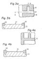
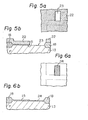
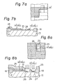
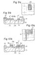
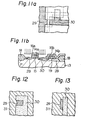
- a second polysilicon layer having a 400 nm thickness is deposited over the entire surface by CVD and is patterned to form the control gate 16 comprising the reading portion 16a and the writing and erasing region 16b.
- the second polysilicon layer 16', the silicon dioxide layer 17' under the second polysilicon layer 16', and the first polysilicon layer 14' are patterned by a double self-alignment process, resulting in the final control gate 16 (16a and 16b), insulating layer between the gates, and floating gate 14 (14a and 14b).
- the pattern of the control gate 16 is shown by a hatched region, and the pattern of the floating gate 17 after the double self-alignment process by a dotted region.
Landscapes
- Non-Volatile Memory (AREA)
- Static Random-Access Memory (AREA)
Applications Claiming Priority (2)
| Application Number | Priority Date | Filing Date | Title |
|---|---|---|---|
| JP174776/82 | 1982-10-05 | ||
| JP57174776A JPS5963763A (ja) | 1982-10-05 | 1982-10-05 | 半導体装置の製造方法 |
Publications (3)
| Publication Number | Publication Date |
|---|---|
| EP0106617A2 true EP0106617A2 (fr) | 1984-04-25 |
| EP0106617A3 EP0106617A3 (en) | 1985-12-11 |
| EP0106617B1 EP0106617B1 (fr) | 1987-07-08 |
Family
ID=15984463
Family Applications (1)
| Application Number | Title | Priority Date | Filing Date |
|---|---|---|---|
| EP83306004A Expired EP0106617B1 (fr) | 1982-10-05 | 1983-10-04 | Procédé de fabrication d'un EEPROM |
Country Status (4)
| Country | Link |
|---|---|
| US (1) | US4517732A (fr) |
| EP (1) | EP0106617B1 (fr) |
| JP (1) | JPS5963763A (fr) |
| DE (1) | DE3372429D1 (fr) |
Cited By (1)
| Publication number | Priority date | Publication date | Assignee | Title |
|---|---|---|---|---|
| EP0610643A1 (fr) * | 1993-02-11 | 1994-08-17 | STMicroelectronics S.r.l. | Cellule EEPROM et transistor MOS périphérique |
Families Citing this family (21)
| Publication number | Priority date | Publication date | Assignee | Title |
|---|---|---|---|---|
| JPS56116670A (en) * | 1980-02-20 | 1981-09-12 | Hitachi Ltd | Semiconductor integrated circuit device and manufacture thereof |
| US4698899A (en) * | 1983-10-19 | 1987-10-13 | Gould Inc. | Field effect transistor |
| JPS60234372A (ja) * | 1984-05-07 | 1985-11-21 | Toshiba Corp | 半導体装置の製造方法 |
| EP0164605B1 (fr) * | 1984-05-17 | 1990-02-28 | Kabushiki Kaisha Toshiba | Procédé de fabrication d'un dispositif EEPROM semi-conducteurs non-volatil |
| NL8402023A (nl) * | 1984-06-27 | 1986-01-16 | Philips Nv | Halfgeleiderinrichting met een niet-vluchtige geheugentransistor. |
| JPS61136274A (ja) * | 1984-12-07 | 1986-06-24 | Toshiba Corp | 半導体装置 |
| US4590665A (en) * | 1984-12-10 | 1986-05-27 | Solid State Scientific, Inc. | Method for double doping sources and drains in an EPROM |
| US4892840A (en) * | 1986-03-27 | 1990-01-09 | Texas Instruments Incorporated | EPROM with increased floating gate/control gate coupling |
| IT1196997B (it) * | 1986-07-25 | 1988-11-25 | Sgs Microelettronica Spa | Processo per realizzare strutture includenti celle di memoria non volatili e2prom con strati di silicio autoallineate transistori associati |
| IT1225873B (it) * | 1987-07-31 | 1990-12-07 | Sgs Microelettrica S P A Catan | Procedimento per la fabbricazione di celle di memoria eprom cmos con riduzione del numero di fasi di mascheratura. |
| US4851361A (en) * | 1988-02-04 | 1989-07-25 | Atmel Corporation | Fabrication process for EEPROMS with high voltage transistors |
| US5262342A (en) * | 1988-11-04 | 1993-11-16 | Mitsubishi Denki Kabushiki Kaisha | Method of making a semiconductor memory device having error checking/correcting functions |
| US4957877A (en) * | 1988-11-21 | 1990-09-18 | Intel Corporation | Process for simultaneously fabricating EEPROM cell and flash EPROM cell |
| JPH0360039U (fr) * | 1989-10-12 | 1991-06-13 | ||
| JP2509717B2 (ja) * | 1989-12-06 | 1996-06-26 | 株式会社東芝 | 半導体装置の製造方法 |
| US5229631A (en) * | 1990-08-15 | 1993-07-20 | Intel Corporation | Erase performance improvement via dual floating gate processing |
| US5147813A (en) * | 1990-08-15 | 1992-09-15 | Intel Corporation | Erase performance improvement via dual floating gate processing |
| US5316981A (en) * | 1992-10-09 | 1994-05-31 | Advanced Micro Devices, Inc. | Method for achieving a high quality thin oxide using a sacrificial oxide anneal |
| US5362685A (en) * | 1992-10-29 | 1994-11-08 | Advanced Micro Devices, Inc. | Method for achieving a high quality thin oxide in integrated circuit devices |
| KR0135047B1 (ko) * | 1994-06-30 | 1998-04-20 | 문정환 | 반도체 읽기 전용 기억 장치의 코딩 방법 |
| US5498577A (en) * | 1994-07-26 | 1996-03-12 | Advanced Micro Devices, Inc. | Method for fabricating thin oxides for a semiconductor technology |
Family Cites Families (7)
| Publication number | Priority date | Publication date | Assignee | Title |
|---|---|---|---|---|
| US4112575A (en) * | 1976-12-20 | 1978-09-12 | Texas Instruments Incorporated | Fabrication methods for the high capacity ram cell |
| US4203158A (en) * | 1978-02-24 | 1980-05-13 | Intel Corporation | Electrically programmable and erasable MOS floating gate memory device employing tunneling and method of fabricating same |
| US4218267A (en) * | 1979-04-23 | 1980-08-19 | Rockwell International Corporation | Microelectronic fabrication method minimizing threshold voltage variation |
| US4332077A (en) * | 1979-08-10 | 1982-06-01 | Rca Corporation | Method of making electrically programmable control gate injected floating gate solid state memory transistor |
| US4409723A (en) * | 1980-04-07 | 1983-10-18 | Eliyahou Harari | Method of forming non-volatile EPROM and EEPROM with increased efficiency |
| US4380057A (en) * | 1980-10-27 | 1983-04-12 | International Business Machines Corporation | Electrically alterable double dense memory |
| US4416708A (en) * | 1982-01-15 | 1983-11-22 | International Rectifier Corporation | Method of manufacture of high speed, high power bipolar transistor |
-
1982
- 1982-10-05 JP JP57174776A patent/JPS5963763A/ja active Granted
-
1983
- 1983-10-04 US US06/538,884 patent/US4517732A/en not_active Expired - Lifetime
- 1983-10-04 EP EP83306004A patent/EP0106617B1/fr not_active Expired
- 1983-10-04 DE DE8383306004T patent/DE3372429D1/de not_active Expired
Cited By (2)
| Publication number | Priority date | Publication date | Assignee | Title |
|---|---|---|---|---|
| EP0610643A1 (fr) * | 1993-02-11 | 1994-08-17 | STMicroelectronics S.r.l. | Cellule EEPROM et transistor MOS périphérique |
| US5637520A (en) * | 1993-02-11 | 1997-06-10 | Sgs-Thomson Microelectronics S.R.L. | Process for fabricating integrated devices including flash-EEPROM memories and transistors |
Also Published As
| Publication number | Publication date |
|---|---|
| US4517732A (en) | 1985-05-21 |
| JPS638631B2 (fr) | 1988-02-23 |
| EP0106617B1 (fr) | 1987-07-08 |
| EP0106617A3 (en) | 1985-12-11 |
| JPS5963763A (ja) | 1984-04-11 |
| DE3372429D1 (en) | 1987-08-13 |
Similar Documents
| Publication | Publication Date | Title |
|---|---|---|
| US4517732A (en) | Method for fabricating an EEPROM | |
| US5872036A (en) | Method of manufacturing a split-gate flash memory cell | |
| US7683423B2 (en) | Semiconductor device including transistor with composite gate structure and transistor with single gate structure, and method for manufacturing the same | |
| JPH08316347A (ja) | リセスチャンネル構造を有する半導体素子及びその製造方法 | |
| KR0138312B1 (ko) | 비휘발성 반도체 메모리장치의 제조방법 | |
| EP0610643B1 (fr) | Cellule EEPROM et transistor MOS périphérique | |
| US6479346B1 (en) | Semiconductor memory device and fabrication method thereof | |
| US6399466B2 (en) | Method of manufacturing non-volatile semiconductor memory device storing charge in gate insulating layer therein | |
| US5385856A (en) | Manufacture of the fieldless split-gate EPROM/Flash EPROM | |
| US20010001490A1 (en) | Device with differential field isolation thicknesses and related methods | |
| KR100261996B1 (ko) | 플래쉬 메모리 셀 및 그의 제조방법 | |
| KR100854504B1 (ko) | 플래쉬 메모리 소자의 제조방법 및 그에 의해 제조된플래쉬 메모리 소자 | |
| US5208173A (en) | Method of manufacturing non-volatile semiconductor memory device | |
| US6075267A (en) | Split-gate non-volatile semiconductor memory device | |
| US6165847A (en) | Nonvolatile semiconductor memory device and method for manufacturing the same | |
| JP3447179B2 (ja) | 不揮発性半導体メモリ装置とその製造方法 | |
| KR0136531B1 (ko) | 반도체장치의 제조방법 | |
| KR100523771B1 (ko) | 불휘발성 반도체 기억 장치 | |
| KR100215888B1 (ko) | 플래쉬 메모리 제조방법 | |
| US6486507B1 (en) | Split gate type memory cell having gate insulating layers appropriately regulated in thickness and process of fabrication thereof | |
| KR100215835B1 (ko) | 플래쉬 메모리 소자 및 그 제조방법 | |
| JPH0147905B2 (fr) | ||
| JP3377386B2 (ja) | 不揮発性半導体記憶装置の製造方法 | |
| JPH0139663B2 (fr) | ||
| KR100299595B1 (ko) | 분할게이트플레쉬메모리셀구조 |
Legal Events
| Date | Code | Title | Description |
|---|---|---|---|
| PUAI | Public reference made under article 153(3) epc to a published international application that has entered the european phase |
Free format text: ORIGINAL CODE: 0009012 |
|
| AK | Designated contracting states |
Designated state(s): DE FR GB |
|
| PUAL | Search report despatched |
Free format text: ORIGINAL CODE: 0009013 |
|
| AK | Designated contracting states |
Designated state(s): DE FR GB |
|
| 17P | Request for examination filed |
Effective date: 19851206 |
|
| 17Q | First examination report despatched |
Effective date: 19860922 |
|
| GRAA | (expected) grant |
Free format text: ORIGINAL CODE: 0009210 |
|
| AK | Designated contracting states |
Kind code of ref document: B1 Designated state(s): DE FR GB |
|
| ET | Fr: translation filed | ||
| REF | Corresponds to: |
Ref document number: 3372429 Country of ref document: DE Date of ref document: 19870813 |
|
| PLBE | No opposition filed within time limit |
Free format text: ORIGINAL CODE: 0009261 |
|
| STAA | Information on the status of an ep patent application or granted ep patent |
Free format text: STATUS: NO OPPOSITION FILED WITHIN TIME LIMIT |
|
| 26N | No opposition filed | ||
| PGFP | Annual fee paid to national office [announced via postgrant information from national office to epo] |
Ref country code: GB Payment date: 19981001 Year of fee payment: 16 |
|
| PGFP | Annual fee paid to national office [announced via postgrant information from national office to epo] |
Ref country code: FR Payment date: 19981009 Year of fee payment: 16 |
|
| PGFP | Annual fee paid to national office [announced via postgrant information from national office to epo] |
Ref country code: DE Payment date: 19981012 Year of fee payment: 16 |
|
| PG25 | Lapsed in a contracting state [announced via postgrant information from national office to epo] |
Ref country code: GB Free format text: LAPSE BECAUSE OF NON-PAYMENT OF DUE FEES Effective date: 19991004 |
|
| GBPC | Gb: european patent ceased through non-payment of renewal fee |
Effective date: 19991004 |
|
| PG25 | Lapsed in a contracting state [announced via postgrant information from national office to epo] |
Ref country code: FR Free format text: LAPSE BECAUSE OF NON-PAYMENT OF DUE FEES Effective date: 20000630 |
|
| PG25 | Lapsed in a contracting state [announced via postgrant information from national office to epo] |
Ref country code: DE Free format text: LAPSE BECAUSE OF NON-PAYMENT OF DUE FEES Effective date: 20000801 |
|
| REG | Reference to a national code |
Ref country code: FR Ref legal event code: ST |