EP0107355A2 - CMIS-Schaltungsanordnung - Google Patents
CMIS-Schaltungsanordnung Download PDFInfo
- Publication number
- EP0107355A2 EP0107355A2 EP83305677A EP83305677A EP0107355A2 EP 0107355 A2 EP0107355 A2 EP 0107355A2 EP 83305677 A EP83305677 A EP 83305677A EP 83305677 A EP83305677 A EP 83305677A EP 0107355 A2 EP0107355 A2 EP 0107355A2
- Authority
- EP
- European Patent Office
- Prior art keywords
- chip
- cmis
- inverter
- circuit device
- series
- Prior art date
- Legal status (The legal status is an assumption and is not a legal conclusion. Google has not performed a legal analysis and makes no representation as to the accuracy of the status listed.)
- Ceased
Links
Images


Classifications
-
- H—ELECTRICITY
- H03—ELECTRONIC CIRCUITRY
- H03K—PULSE TECHNIQUE
- H03K19/00—Logic circuits, i.e. having at least two inputs acting on one output; Inverting circuits
- H03K19/0008—Arrangements for reducing power consumption
- H03K19/0016—Arrangements for reducing power consumption by using a control or a clock signal, e.g. in order to apply power supply
-
- G—PHYSICS
- G11—INFORMATION STORAGE
- G11C—STATIC STORES
- G11C8/00—Arrangements for selecting an address in a digital store
- G11C8/18—Address timing or clocking circuits; Address control signal generation or management, e.g. for row address strobe [RAS] or column address strobe [CAS] signals
-
- H—ELECTRICITY
- H03—ELECTRONIC CIRCUITRY
- H03K—PULSE TECHNIQUE
- H03K19/00—Logic circuits, i.e. having at least two inputs acting on one output; Inverting circuits
- H03K19/02—Logic circuits, i.e. having at least two inputs acting on one output; Inverting circuits using specified components
- H03K19/08—Logic circuits, i.e. having at least two inputs acting on one output; Inverting circuits using specified components using semiconductor devices
- H03K19/094—Logic circuits, i.e. having at least two inputs acting on one output; Inverting circuits using specified components using semiconductor devices using field-effect transistors
- H03K19/096—Synchronous circuits, i.e. using clock signals
- H03K19/0963—Synchronous circuits, i.e. using clock signals using transistors of complementary type
Definitions
- the present invention relates to a complementary metal-insulator semiconductor (CMIS) circuit device and in particular to a CMIS circuit device wherein an integrated circuit (IC) chip thereof can be selected by input signals at least two of which have opposite polarities.
- CMIS complementary metal-insulator semiconductor
- a plurality of IC chips of semiconductor memories and so on are used in one system, such as a computer, for the purpose of increasing the memory capacity.
- a desired IC chip is selected from a plurality of IC chips for data reading or writing by a chip-select signal.
- a CMIS circuit device the state of which is controlled by at least two input signals and which is made selectable on receiving input signals at least two of which have opposite polarities has a chip-select control circuit for establishing a chip-selected state and a chip-unselected state in accordance with the received input signals, the chip-select control circuit comprising CMIS inverter means for inverting one of the input signals and CMIS logic gate means for receiving an output signal of the CMIS inverter means and the other input signal or signals and for outputting an internal chip-select control signal, wherein the CMIS inverter means comprises a CMIS inverter and one or more control transistors receiving the other input signal or signals at the gates thereof and which are inserted in series between a power terminal of the CMIS inverter and a power source.
- the present invention utilizes the concept of inserting one or more series-connected transistors between a power terminal of a first inverter, which inverts one input or chip-select signal, and a power source and of controlling each series-connected transistor with another input or chip-select signal.
- One advantage of the present invention is to make it possible in a CMIS circuit device to obtain a condition in which a circuit current does not flow at all and to realize a complete battery backup condition when an IC chip is caused to assume an unselected state by making at least one of two chip-select signals having opposite polarities approximately equal to the power supply voltage or the ground voltage.
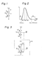
- Figure 1 shows a typical CMIS inverter circuit.
- the circuit of Fig. 1 is composed of a P-channel metal--insulator semiconductor (MIS) transistor Ql and an N-channel MIS transistor Q2 which are serially connected between a power source V CC , having, for example, a positive voltage, and the ground.
- MIS metal--insulator semiconductor
- V CC power source
- the threshold voltage of the transistor Q2 is V th (N)
- the threshold voltage of the transistor Ql is V th (P)
- a direct current flows through the circuit provided that the level V CS of an input signal CS falls within a range represented as V th (N) ⁇ V CS ⁇ V CC -
- the transistor Ql is in an ON state and the transistor Q2 is in a completely OFF state.
- the current I becomes zero.
- the transistor Q2 gradually assumes an ON state so that the current I gradually begins to flow and then gradually increases.
- the current I reaches a peak value because both transistors Ql and Q2 exhibit a comparatively low-resistance state.
- an input level of a CMIS integrated circuit device is prescribed in a specification as a minimum value V IH of the high--level voltage and a maximum value V IL of the low-level voltage.
- V IH is 2 . 0 to 2 .4 volts and VIL is approximately 0.8 volts.
- V IH is 2 . 0 to 2 .4 volts and VIL is approximately 0.8 volts.
- Such a CMIS integrated circuit device must operate as if a low-level voltage is applied thereto when the input voltage does not exceed V IL and as if a high-level voltage is applied thereto when the input voltage is not lower than V IH .
- the voltages V IL and V IH thus prescribed exist within a range in which a direct current I shown in Fig. 1 flows.
- Figure 3 shows part of another conventional integrated circuit device in which the drawback of the above-mentioned conventional device has been removed.
- one or more input circuitsIPCto which an input signal IN, such as an address signal or data signal, is applied are controlled by a CMIS inverter for chip selection which is composed of a P-channel transistor Q3 and an N-channel transistor Q4.
- the input circuit or circuits IPC are composed of a P-channel transistor Q5, a P-channel transistor Q6, and a parallel circuit consisting of an N-channel transistor Q7 and an N-channel transistor Q8 which are serially connected between the power source V CC and the ground.
- the input signal IN is applied to the gates of the transistors Q6 and Q7.
- An output signal IN is derived from the point where the transistor Q6 and the parallel circuit are coupled and is fed to a circuit within the integrated circuit device.
- the gates of the transistors Q5 and Q8 are connected to the output of the inverter circuit for chip selection, which circuit outputs the signal CS.
- the inverted chip-select signal CS assumes a level which is approximately V CC . Accordingly, the transistor Q5 in the input circuit IPC is turned off and the transistor Q8 is turned on. No matter what state the input signal IN may assume, the inverted input signal IN becomes 0 volts. In this case, no direct current flows through any circuit. Even in a multiple-input integrated circuit device, it is possible to attain a battery backup condition by using the circuit illustrated in Fig. 3 and by setting one chip-select signal CS at 0 volts.
- each 1C chip when a plurality of memory chips are used in a system such as a computer, it is advantageous in the system configuration for each 1C chip to have two chip-select inputs, thereby enabling a battery backup condition to be attained.
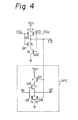
- Figure 4 shows part of the configuration of an integrated circuit device wherein, an IC chip thereof can be selected by using two chip-select signals CS 1 and CS 2 .
- a chip--select inverter comprises a parallel circuit composed of P-channel transistors Q9 and Q10, an N-channel transistor Qll, and an N-channel transistor Q12, all of which are connected in series between the power source V CC and the ground.
- the first chip-select signal CS 1 is applied to the gates of the transistor Q9 and the transistor Qll and the second chip select signal CS 2 is applied to the gates of the transistors Q10 and Q12.
- the inverted internal chip-select signal CS for controlling the input circuit IPC which is the same as the circuit illustrated in Fig. 3, is derived from a point where the parallel circuit composed of transistors Q9 and Q10 is connected to the transistor Qll.
- Figure 5 shows part of the configuration of an integrated circuit device wherein an IC chip thereof can be selected by using two inverted select signals CS 1 and CS 2 .
- the circuit illustrated in Fig. 5 is equipped with a first inverter, which is composed of a P-channel transistor Q13, a P-channel transistor Q14, and a parallel circuit consisting of N-channel transistors Q15 and Q16 connected in series, and a second inverter which receives the output of the first inverter and is composed of a P-channel transistor Q17 and an N-channel transistor Q18. From the output terminal of the second inverter, an inverted internal chip-select signal CS is output to control the input circuit IPC, which is the same as the circuit illustrated in Fig. 3.
- a battery backup condition can be established by setting at least one of the two inverted chip-select signals CS 1 and CS 2 at a level near the power source voltage V CC .
- the two chip-select signals In the integrated circuit devices illustrated in Fig. 4 and Fig. 5, the two chip-select signals must have an identical polarity. Recently, it has been desired, in an integrated circuit device to which two chip-select signals having opposite polarities are applied, that a battery backup condition be attained by arbitrarily using one of the two chip-select signals. Accordingly, a circuit configuration as illustrated in Fig. 6 has been proposed. The circuit illustrated in Fig.
- a first inverter composed of a P-channel transistor Q20 and an N-channel transistor Q21
- a second inverter composed of P-channel transistors Q23 and Q24 and a parallel circuit consisting of two N-channel transistors Q25 and Q26
- a third inverter composed of a P-channel transistor Q27 and an N-channel transistor Q28.
- An inverted chip-select signal CS for controlling the input circuit IPC which is the same as the circuit illustrated in Fig. 3, is fed from the output of the third inverter.
- a chip-select signal CS l is applied to the gates of transistors Q24 and Q26 of the second inverter, and a chip-select signal CS 2 is applied to the gates of transistors Q20 and Q21 of the first inverter.
- the input circuit IPC can be activated and caused to assume a chip-selected state by causing the chip-select signal CS l to assume a low level and by causing the chip-select signal CS 2 to assume a high level so that the inverted chip-select signal CS assumes a low level. If the chip-select signal CS 1 is caused to assume a high level or the chip-select signal CS 2 is caused to assume a low level, the inverted chip-select signal CS is caused to assume a high level and the input circuit IPC is rendered to be in an inactive state. As a result, the inverted input signal IN is always at a low level, and a chip--unselected state is attained.
- the inverted chip-select signal CS can be caused to assume a high level which is near the power source voltage V CC .
- the current flowing through the input circuit IPC can be decreased to zero.
- the N-channel transistor Q21 is turned off in the first inverter.
- the P-channel transistor Q23 is turned off irrespective of the state of the chip-select signal CS 1 .
- the N-channel transistor Q28 is turned off. Therefore, no current flows through any inverter.
- a battery backup condition may be completely attained by controlling only the chip-select signal CS 2 of the two chip-select signals CS l and CS 2 .
- the circuit illustrated in Fig. 6 has a drawback in that the chip-select signal CS 2 must be set at a level near the ground level in order to completely reduce to zero the current flowing through the first inverter. That is if chip-select signal CS 1 is at V CC and the chip-select signal CS 2 is at V IL , for example, the N-channel transistor Q21 in the first inverter does not completely turn off.
- the circuit illustrated in Fig. 6 has a further drawback in that it is impossible to attain a battery backup condition by controlling only one of the two chip-select signals CS 1 and CS 2 having opposite polarities.
- FIG. 7 shows part of the configuration of a CMIS circuit device which is an embodiment of the present invention.
- the circuit of Fig. 7 includes a chip-select control circuit for feeding an inverted internal chip-select signal CS to an input circuit IPC, which is the same as the circuit illustrated in Fig. 3.
- the chip-select control circuit comprises three inverter circuits IV 1 , IV 2 , and IV 3 .
- the first inverter circuit IV 1 comprises a P-channel transistor Q19, a P-channel transistor Q20, and an N-channel transistor Q21 which are serially connected between a power source V CC and the ground.
- a first chip-select signal CS l is applied to the gate of the transistor Q19 and a second chip-select signal CS 2 is applied to the gates of the transistors Q20 and Q21.
- the output of the first inverter IV 1 is derived from the point where the transistors Q20 and Q21 are coupled and is fed to the second inverter IV 2 .
- the second inverter IV 2 is practically constructed as a two-input NOR gate circuit.
- a P-channel transistor Q23, a P-channel transistor Q24, and a parallel circuit composed of an N-channel transistor Q25 and an N-channel transistor Q26 are connected in series between the power source V CC and the ground.
- the output signal of the first inverter is applied to the gates of the transistors Q23 and Q25.
- the first chip-select signal CS l is applied to the gates of the transistors Q24 and Q26.
- the third inverter IV 3 comprises a P-channel transistor Q27 and an N-channel transistor Q28 which are connected in series between the power source V CC and the ground.
- an internal chip-select signal CS is applied to the gates of the transistors Q27 and Q28.
- An inverted internal chip-select signal CS is derived from a point where the transistors Q27 and Q28 are coupled and is fed to the input circuit IPC.
- Figure 8 shows the circuit status for various levels of the two chip-select signals CS1 and CS 2 .
- the operation of the circuit illustrated in Fig. 7 is described with reference to Fig. 8.
- L denotes a voltage near zero volts, i.e., a voltage within the region A illustrated in Fig. 2
- H denotes a voltage near the power source voltage V CC , i.e., a voltage within the region B illustrated in Fig. 2.
- V IL and V IH are, respectively, the same as those illustrated in Fig. 2.
- V IL is 0.8 volts and V IH is 2.0 to 2.4 volts.
- the chip-select signal CS 1 must be at a low level, i.e., L or V IL , and, at the same time, the chip-select signal CS 2 must be at a high level, i.e., H or V IH .
- the transistors Q19 and Q21 of the first inverter IV l turn on and the transistor Q20 turns off so that the potential at point a becomes an L level.
- the transistor Q23 in the second inverter IV 2 turns on and the transistor Q25 turns off.
- the level of the output of the second inverter IV 2 i.e., the level at point b
- the output CS of the third inverter IV 3 assumes a low level.
- a transistor Q5 turns on and a transistor Q8 turns off. Therefore, the input circuit IPC functions as an ordinary CMIS inverter and a chip-selected state is attained.
- the inverted chip-select signal CS assumes an H level and a chip-unselected state is attained. That is, when both of the chip-select signals ES 1 and CS 2 are at a low level, i.e., at an L or V IL level, both of the transistors Q19 and Q20 in the first inverter IV 1 turn on and the level at point a becomes an H level. As a result, the transistor Q25 in the second inverter IV 2 turns on and the level at point b becomes an L level.
- the inverted chip-select signal CS assumes an H level so that the transistor Q5 in the input circuit IPC turns off and the transistor Q8 turns on.
- the inverted input signal IN assumes a low level and a chip-unselected state is attained.
- the chip-select signal CS 2 is at an L level
- the transistor Q21 in the first inverter IV 1 is completely turned off so that no cURRENT I 1 flows through the first inverter IV 1 .
- the level at point a is an H level
- the transistor Q23 in the second inverter IV 2 is completely turned off and no currentI 2 flows therethrough.
- the signal at point b i.e., the input signal
- assumes an L level the transistor Q28 is completely turned off so that no current flows therethrough.
- both chip-select signals CS 1 and CS 2 are at a high level, i.e., H or V IH , the transistor Q21 in the first inverter IV 1 turns on and the level at point a becomes an L level. Since the transistor Q26 in the second inverter IV 2 turns on, the level at point b also becomes an L level. As a result, the inverted chip-select signal CS assumes an H level and a chip--unselected state is attained.
- both the transistor Q19 in the first inverter IV 1 and the transistor Q24 in the second inverter IV 2 are completely turned off and no current I 1 ,I 2 flows through the first and second inverters.
- the chip-select signal CS 1 is at a high level, i.e., H or V IH
- the chip-select signal CS 2 is at a low level, i.e., L or V IH
- the chip-select signal CS 1 is at an H level and the chip-select signal CS 2 is at an L level
- both of the transistors Q19 and Q21 in the first inverter IV 1 are completely turned off. Therefore, no current I 1 flows through the first inverter IV 1 and the output terminal thereof, i.e., point a assumes a floating state.
- the transistor Q26 turns on and the transistor Q24 is completely turned off.
- the level at point b becomes an L level and no current I 2 flows through the second inverter IV 2 .
- the chip-select signal CS 1 is V IH and the chip--select signal CS 2 is L
- the transistor Q21 in the first inverter IV 1 is completely turned off.
- the transistor Q20 turns on and the transistor Q19 is in a slightly conductive state.
- the level at point a becomes an H level, thereby preventing currently from flowing through the first inverter IV 1 . Since, in this case, the transistor Q25 in the second inverter IV 2 is turned on, point b assumes an L level and no current I 2 flows through the second inverter IV 2 because the transistor Q23 is completely turned off.
- the transistor Q19 in the first inverter IV 1 assumes a somewhat conductive state
- the transistor Q20 turns on
- the transistor Q21 assumes a somewhat conductive state. Therefore, point a assumes an intermediate value between the power source voltage V CC and 0 volts.
- the current I 1 flowing through the first inverter IV 1 does not assume a zero value. Since, in this case, the transistor Q26 in the second inverter IV 2 is turned on, point b assumes an L level. However, the current I 2 flowing through the second inverter IV 2 is not reduced to zero.
- the second inverter IV 2 is constructed as a NOR gate circuit. That is, the NOR logic output of the inverted chip--select signal CS 1 and the output signal of the first inverter IV 1 is used as the internal chip-select control signal CS.
- the NOR gate circuit can be replaced with a NAND gate circuit, to which the non-inverted chip-select signal CS 1 or CS 2 is applied.
- the inverted external chip-select signal CS 1 or CS 2 is inverted in the first inverter.
- the output of the first inverter and the remaining chip-select signal CS 2 or CS 1 are fed to the above-mentioned NAND gate circuit to produce the inverted internal chip-select signal CS.
- the feature of the present invention lies in the fact that the remaining chip-select signal CS 2 or CS 1 is fed to the gate of a transistor which is inserted between a power terminal of the first inverter and a power source.
- the transistor receiving the chip-select signal CS 2 or CS 1 may be an N-channel MIS transistor inserted into the first inverter in series with the driver transistor thereof.
- the current of the circuits including the first inverter can be made to be substantially zero no matter what level the remaining chip-select signal may assume. Thus, a complete battery backup condition can be realized.
- Figure 10 illustrates another modified embodiment showing how the MIS circuit devj ce may be selected bv three or more chip-select signals.
- the number of transistors Q19 and Q32 inserted into the first inverter is increased in accordance with the number of chip-select signals and the number of logic inputs applied to the second inverter (NOR or NAND gate) is also increased.
Landscapes
- Engineering & Computer Science (AREA)
- Physics & Mathematics (AREA)
- Computer Hardware Design (AREA)
- Computing Systems (AREA)
- General Engineering & Computer Science (AREA)
- Mathematical Physics (AREA)
- Microelectronics & Electronic Packaging (AREA)
- Power Engineering (AREA)
- Logic Circuits (AREA)
- Electronic Switches (AREA)
Applications Claiming Priority (2)
| Application Number | Priority Date | Filing Date | Title |
|---|---|---|---|
| JP167511/83 | 1982-09-28 | ||
| JP57167511A JPS5957525A (ja) | 1982-09-28 | 1982-09-28 | Cmis回路装置 |
Publications (2)
| Publication Number | Publication Date |
|---|---|
| EP0107355A2 true EP0107355A2 (de) | 1984-05-02 |
| EP0107355A3 EP0107355A3 (de) | 1986-12-17 |
Family
ID=15851033
Family Applications (1)
| Application Number | Title | Priority Date | Filing Date |
|---|---|---|---|
| EP83305677A Ceased EP0107355A3 (de) | 1982-09-28 | 1983-09-23 | CMIS-Schaltungsanordnung |
Country Status (3)
| Country | Link |
|---|---|
| US (1) | US4581549A (de) |
| EP (1) | EP0107355A3 (de) |
| JP (1) | JPS5957525A (de) |
Cited By (2)
| Publication number | Priority date | Publication date | Assignee | Title |
|---|---|---|---|---|
| EP0453997A1 (de) * | 1990-04-21 | 1991-10-30 | Kabushiki Kaisha Toshiba | Halbleiter-Speichereinrichtung |
| EP0342592A3 (de) * | 1988-05-16 | 1992-02-19 | Kabushiki Kaisha Toshiba | Chipfreigabe-Eingangsschaltung in einer Halbleiterspeicheranordnung |
Families Citing this family (5)
| Publication number | Priority date | Publication date | Assignee | Title |
|---|---|---|---|---|
| US4649299A (en) * | 1984-04-16 | 1987-03-10 | National Semiconductor Corporation | Strobe line driver circuit |
| JPS61262827A (ja) * | 1985-05-15 | 1986-11-20 | Mitsubishi Electric Corp | 半導体集積回路装置 |
| KR880009375A (ko) * | 1987-01-17 | 1988-09-15 | 강진구 | 씨모오스 어드레스 버퍼 |
| JP2728533B2 (ja) * | 1990-01-19 | 1998-03-18 | 富士通株式会社 | 半導体装置 |
| CN107241252B (zh) * | 2017-06-30 | 2022-09-23 | 珠海格力电器股份有限公司 | Can通讯极性控制电路和系统及多联空调系统 |
Family Cites Families (4)
| Publication number | Priority date | Publication date | Assignee | Title |
|---|---|---|---|---|
| JPS568435B2 (de) * | 1972-09-19 | 1981-02-24 | ||
| US4337525A (en) * | 1979-04-17 | 1982-06-29 | Nippon Electric Co., Ltd. | Asynchronous circuit responsive to changes in logic level |
| JPS56111180A (en) * | 1980-02-06 | 1981-09-02 | Toshiba Corp | Semiconductor device |
| JPS58164322A (ja) * | 1982-03-24 | 1983-09-29 | Toshiba Corp | 半導体入力回路装置 |
-
1982
- 1982-09-28 JP JP57167511A patent/JPS5957525A/ja active Pending
-
1983
- 1983-09-23 EP EP83305677A patent/EP0107355A3/de not_active Ceased
- 1983-09-26 US US06/535,833 patent/US4581549A/en not_active Expired - Lifetime
Cited By (3)
| Publication number | Priority date | Publication date | Assignee | Title |
|---|---|---|---|---|
| EP0342592A3 (de) * | 1988-05-16 | 1992-02-19 | Kabushiki Kaisha Toshiba | Chipfreigabe-Eingangsschaltung in einer Halbleiterspeicheranordnung |
| EP0453997A1 (de) * | 1990-04-21 | 1991-10-30 | Kabushiki Kaisha Toshiba | Halbleiter-Speichereinrichtung |
| US5355331A (en) * | 1990-04-21 | 1994-10-11 | Kabushiki Kaisha Toshiba | Semiconductor memory device having electrically isolated memory and logic sections |
Also Published As
| Publication number | Publication date |
|---|---|
| US4581549A (en) | 1986-04-08 |
| JPS5957525A (ja) | 1984-04-03 |
| EP0107355A3 (de) | 1986-12-17 |
Similar Documents
| Publication | Publication Date | Title |
|---|---|---|
| US4841233A (en) | Semiconductor integrated circuit adapted to carry out operation test | |
| EP0301588A2 (de) | Halbleiterspeicheranordnung | |
| US4565932A (en) | High voltage circuit for use in programming memory circuits (EEPROMs) | |
| EP0347530A2 (de) | Statische RAM-Speicheranordnung mit einer Leistungsverminderungsfunktion | |
| US4441169A (en) | Static random access memory having a read out control circuit connected to a memory cell | |
| KR950007449B1 (ko) | 메모리의 출력 버퍼 회로 | |
| US4432049A (en) | Programmable mode select by reset | |
| US3644907A (en) | Complementary mosfet memory cell | |
| EP0009862A1 (de) | Programmierbare Betriebsartauswahl durch Rücksetzen und diese Auswahl verwendende Datenverarbeitungsanlage | |
| US4864541A (en) | Integrated circuit of the logic circuit type comprising an electrically programmable non-volatile memory | |
| EP0107355A2 (de) | CMIS-Schaltungsanordnung | |
| US4970693A (en) | Semiconductor memory device with internal control signal based upon output timing | |
| US4504926A (en) | Mode setting control system | |
| US4198700A (en) | Column decode circuit for random access memory | |
| EP0440176B1 (de) | Halbleiterspeicheranordnung | |
| EP0019381A1 (de) | Halbleiterspeicher mit Adressensignalpegeleinstellung | |
| EP0063357B1 (de) | Treiberschaltung | |
| KR100207971B1 (ko) | 전위 전송회로 및 이를 이용한 반도체 장치 | |
| US5021680A (en) | Voltage supply circuit for programming circuits of programmable logic arrays | |
| JPH03105797A (ja) | デコーダ回路 | |
| US4482822A (en) | Semiconductor chip selection circuit having programmable level control circuitry using enhancement/depletion-mode MOS devices | |
| US4446386A (en) | MOS Decoder circuit using phase clocking for reducing the power consumption | |
| US4567575A (en) | Voltage level compensating interface circuit for inter-logic circuit data transmission system | |
| US5959902A (en) | Voltage level shifter device, particulary for a nonvolatile memory | |
| EP0114210A2 (de) | Latente Bildspeicherzelle |
Legal Events
| Date | Code | Title | Description |
|---|---|---|---|
| PUAI | Public reference made under article 153(3) epc to a published international application that has entered the european phase |
Free format text: ORIGINAL CODE: 0009012 |
|
| AK | Designated contracting states |
Designated state(s): DE FR GB |
|
| PUAL | Search report despatched |
Free format text: ORIGINAL CODE: 0009013 |
|
| AK | Designated contracting states |
Kind code of ref document: A3 Designated state(s): DE FR GB |
|
| 17P | Request for examination filed |
Effective date: 19870319 |
|
| 17Q | First examination report despatched |
Effective date: 19871125 |
|
| STAA | Information on the status of an ep patent application or granted ep patent |
Free format text: STATUS: THE APPLICATION HAS BEEN REFUSED |
|
| 18R | Application refused |
Effective date: 19900426 |
|
| APAF | Appeal reference modified |
Free format text: ORIGINAL CODE: EPIDOSCREFNE |
|
| RIN1 | Information on inventor provided before grant (corrected) |
Inventor name: YAMAUCHI, TAKAHIKO Inventor name: SEKI, TERUO Inventor name: AOYAMA, KEIZO |