EP0107773A1 - Abschaltbarer Thyristor - Google Patents
Abschaltbarer Thyristor Download PDFInfo
- Publication number
- EP0107773A1 EP0107773A1 EP83109015A EP83109015A EP0107773A1 EP 0107773 A1 EP0107773 A1 EP 0107773A1 EP 83109015 A EP83109015 A EP 83109015A EP 83109015 A EP83109015 A EP 83109015A EP 0107773 A1 EP0107773 A1 EP 0107773A1
- Authority
- EP
- European Patent Office
- Prior art keywords
- region
- invention according
- gate electrode
- electrode
- insulating layer
- Prior art date
- Legal status (The legal status is an assumption and is not a legal conclusion. Google has not performed a legal analysis and makes no representation as to the accuracy of the status listed.)
- Granted
Links
Images
Classifications
-
- H—ELECTRICITY
- H10—SEMICONDUCTOR DEVICES; ELECTRIC SOLID-STATE DEVICES NOT OTHERWISE PROVIDED FOR
- H10D—INORGANIC ELECTRIC SEMICONDUCTOR DEVICES
- H10D64/00—Electrodes of devices having potential barriers
- H10D64/60—Electrodes characterised by their materials
- H10D64/66—Electrodes having a conductor capacitively coupled to a semiconductor by an insulator, e.g. MIS electrodes
- H10D64/68—Electrodes having a conductor capacitively coupled to a semiconductor by an insulator, e.g. MIS electrodes characterised by the insulator, e.g. by the gate insulator
- H10D64/681—Electrodes having a conductor capacitively coupled to a semiconductor by an insulator, e.g. MIS electrodes characterised by the insulator, e.g. by the gate insulator having a compositional variation, e.g. multilayered
- H10D64/685—Electrodes having a conductor capacitively coupled to a semiconductor by an insulator, e.g. MIS electrodes characterised by the insulator, e.g. by the gate insulator having a compositional variation, e.g. multilayered being perpendicular to the channel plane
-
- H—ELECTRICITY
- H10—SEMICONDUCTOR DEVICES; ELECTRIC SOLID-STATE DEVICES NOT OTHERWISE PROVIDED FOR
- H10D—INORGANIC ELECTRIC SEMICONDUCTOR DEVICES
- H10D18/00—Thyristors
- H10D18/60—Gate-turn-off devices
- H10D18/65—Gate-turn-off devices with turn-off by field effect
- H10D18/655—Gate-turn-off devices with turn-off by field effect produced by insulated gate structures
-
- H—ELECTRICITY
- H10—SEMICONDUCTOR DEVICES; ELECTRIC SOLID-STATE DEVICES NOT OTHERWISE PROVIDED FOR
- H10D—INORGANIC ELECTRIC SEMICONDUCTOR DEVICES
- H10D64/00—Electrodes of devices having potential barriers
- H10D64/20—Electrodes characterised by their shapes, relative sizes or dispositions
- H10D64/27—Electrodes not carrying the current to be rectified, amplified, oscillated or switched, e.g. gates
- H10D64/311—Gate electrodes for field-effect devices
-
- H—ELECTRICITY
- H10—SEMICONDUCTOR DEVICES; ELECTRIC SOLID-STATE DEVICES NOT OTHERWISE PROVIDED FOR
- H10D—INORGANIC ELECTRIC SEMICONDUCTOR DEVICES
- H10D64/00—Electrodes of devices having potential barriers
- H10D64/60—Electrodes characterised by their materials
- H10D64/62—Electrodes ohmically coupled to a semiconductor
-
- H—ELECTRICITY
- H10—SEMICONDUCTOR DEVICES; ELECTRIC SOLID-STATE DEVICES NOT OTHERWISE PROVIDED FOR
- H10D—INORGANIC ELECTRIC SEMICONDUCTOR DEVICES
- H10D64/00—Electrodes of devices having potential barriers
- H10D64/60—Electrodes characterised by their materials
- H10D64/66—Electrodes having a conductor capacitively coupled to a semiconductor by an insulator, e.g. MIS electrodes
- H10D64/68—Electrodes having a conductor capacitively coupled to a semiconductor by an insulator, e.g. MIS electrodes characterised by the insulator, e.g. by the gate insulator
- H10D64/693—Electrodes having a conductor capacitively coupled to a semiconductor by an insulator, e.g. MIS electrodes characterised by the insulator, e.g. by the gate insulator the insulator comprising nitrogen, e.g. nitrides, oxynitrides or nitrogen-doped materials
Definitions
- the present invention is related to the following U.S.Patent applications, commonly assigned to the instant assignee: Serial No. 391,620, filed June 24, 1982, by V.A.K. Temple (the inventor herein); Serial No. 345,290, filed February 3, 1982 by V.A.K. Temple (the inventor herein); and Serial No.(Docket RD-14,244), filed contemporaneously herewith, by V.A.K. Temple (the inventor herein).
- Serial No. 391,620 filed June 24, 1982, by V.A.K. Temple (the inventor herein)
- Serial No. 345,290 filed February 3, 1982 by V.A.K. Temple (the inventor herein)
- Serial No.(Docket RD-14,244) filed contemporaneously herewith, by V.A.K. Temple (the inventor herein).
- the entirety of the disclosures of each of the foregoing applications is hereby incorporated by reference.
- the present invention relates to a thyristor, and, more particularly, to a thyristor incorporating metal-oxide-semiconductor ("MOS") structure for facilitating turn-off of the thyristor.
- MOS metal-oxide-semiconductor
- Thyristors are four-region(e.g., P-N-P-N) semiconductor devices that are well-known and typically comprise a P + (or highly-doped P-type) emitter region, an N - (lightly doped N-type) base region, a P (or P-type, of a reference doping level) base region and an N + emitter region, along with an anode connected to the P emitter region and a cathode connected to the N + emitter region.
- a thyristor is "turned-on” when it provides a high conductance between its anode and cathode, and is “turned-off” when it provides a non-conducting path between such electrodes.
- the MOS structure is effective to create an inversion channel in the N emitter region that completes a distributed current path from the P base region of the device to a further P + region of the device, which is ohmically connected to the cathode.
- the inversion channel is conductive to holes, and hole current that flows therein from the P base region to the cathode (via the further P region) facilitates turn-off of the thyristor.
- the inclusion of the further P region in the thyristor necessitates the critical alignment of a photolithographic mask in forming such region.
- a thyristor complementary in structure to that described above can be fabricated by substituting P-type material for N-type material, and vice-versa.
- a thyristor having MOS structure for transporting in a distributed current path, majority carriers from an inner base region of the device to a main current-carrying electrode of the device, wherein the thyristor does not require a further distinct semiconductor region in such distributed current path.
- I provide a thyristor having a P emitter region, an N base region, a P base region, and an N + emitter region.
- An anode adjoins the P emitter region, and a cathode adjoins the N + emitter region.
- An MOS structure is included for transporting holes from the P base region to the cathode.
- the MOS structure includes an insulating layer and a gate electrode. The insulating layer adjoins the N + emitter region and a portion of the cathode which adjoins the N + emitter region.
- the gate to both + electrode is situated adjacent/the N emitter region and such portion of the cathode, but is spaced from the N + emitter region and such portion of the cathode by the insulating layer. complete
- the thyristor does not require a further P region to/a hole current path extending from the P base region to the cathode.
- the thyristor may conveniently be referred to as a metal-oxide-semiconductor turn-off thyristor("MOSTOT").
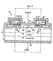
- FIGURE 1 a cross-section of a portion of a MOSTOT 10 incorporating my invention.
- MOSTOT 10 includes a cell or repeated structure 12, which is typically round or rectangular as viewed from above the device. Many cells identical to cell 12 are typically included in MOSTOT 10.
- MOSTOT 10 includes a body 14 of semiconductor material, preferably silicon.
- body 14 includes a P + emitter region 16, an N base region 18, a P base region 20, and an N + emitter region 22, as well as further N emitter regions, such as regions 24 and 26, for further cells.
- MOSTOT 10 has a doping profile, taken vertically through regions 16, 18, 20, and 22, which is selected to yield good thyristor performance.
- MOS structure 30 for transporting holes from P base region 20 to cathode 28, so as to facilitate turn-off of MOSTOT 10.
- MOS structure 30 comprises a gate electrode 31, an insulating layer 32 having component layers 34, 36, and 38, and portion 40 of N + emitter region 22, which is in the vicinity of gate electrode 31.
- Gate electrode 31 preferably comprises a conductive refractory material such as highly-doped polysilicon or molybdenum silicide, known conductive equivalents to metal.
- Component insulating layers 34 and 36 preferably each comprise an oxide of semiconductor material, while component layer 38 preferably comprises silicon nitride, a known dielectric equivalent of oxide, to facilitate the fabrication of MOSTOT 10, as discussed below.
- biasing of gate electrode 30 with a negative voltage above a threshold magnitude results in portion 40 of N + emitter region 22 becoming "inverted", or more populated by holes than electrons, so as to become conductive to holes.
- the inversion channel thus formed in N + emitter portion 40 constitutes part of a distributed current path 42, which extends from the interior of P base region 20 to cathode 28, via the inversion channel in N + emitter portion 40. If, through biasing of gate electrode 31, the electric field induced in further portion 48 of N + emitter region 22 is sufficiently strong, then such further portion 48 becomes inverted and, together with the inversion channel in portion 40, completes distributed current path 42 from P base region 20 to cathode 28.
- the electric field in portion 48 is not strong enough to invert portion 48. Rather, the electric field in portion 48 is only sufficient to deplete portion 48 of mobile electrons, but not to cause portion 48 to become more populated by holes than electrons. Such depleted condition of portion 48 will be understood by those skilled in the art as depletion region punch-through in portion 48 from portion 40 to cathode 28.
- the thickness of insulating layer 34 between gate electrode 31 and cathode 28 can be minimized, provided that the dielectric function of layer 34 is not impaired.
- the thickness of insulating layers 36 and 38 can be minimized, provided that the dielectric function of these layers is not impaired.
- the magnitude of the biasing voltage on gate electrode 31 can be maximized, provided that the dielectric function of insulating layer 32, which surrounds gate electrode 31, is not impaired.
- portion 48 can be limited so as to decrease the level of biasing voltage on gate electrode 31 at which portion 48 becomes depleted of electrons.
- a preferred dopant concentration for portion 48 is below about 10 17 impurity atoms per cubic centimeter, although it could suitably be as high as about 10 18 impurity atoms per cubic centimeter in some embodiments of MOSTOT 10.
- N + emitter portion 48 Limiting the dopant concentration of N + emitter portion 48 to attain the foregoing purpose is likely to result in the portion of junction 50 between portion 48 and cathode 28 constituting a Schottky barrier rectifying contact for electrons.
- at least part of junction 50, between N + emitter region 22 and cathode 28 must form an ohmic contact. This requires that at least some portion of N + emitter region 22 adjoining cathode 28 at junction 50 have a dopant concentration in excess of about 10 17 impurity atoms per cubic centimeter, and, preferably, above about 10 19 impurity atoms per cubic centimeter, due to a localized N + diffusion in region 22, for example.
- junction 50 must not constitute a Schottky barrier rectifying contact for holes; otherwise, distributed current path 42 would not be complete. Accordingly, cathode 28 must comprise a conductive material with a low work function, such as aluminum or titanium. Conversely, if a complementary MOSTOT 10 were fabricated, in which N-type material were used instead of P-type material, and vice-versa,and its corresponding bypass current path were conductive to electrons rather than holes, its cathode would need to comprise a conductive material with a high work function, such as gold or platinum, so as to avoid a Schottky rectifying barrier to electrons.
- Cell 12 of MOSTOT 10 can be turned off when distributed current path 42 has a resistance sufficiently low to prevent P-N junction 44, between P base region 20 and N + emitter region 22, from becoming forward biased, owing to hole current flow in current path 42, by more than about one-half of the energy bandgap voltage of the semiconductor material forming P-N junction 44 (i.e., about 1.0 volt in silicon). If the resistance of current path 42 exceeds such a value, cell 12 cannot turn-off, at least without commutation (i.e., by reversal of the anode 46-to-cathode 28 voltage of MOSTOT 10). In the latter case, turn-off of cell 12 is markedly faster than by commutation alone. In order for the entire MOSTOT 10 to turn-off, each of its cells must turn-off.
- P + emitter region 16, N - base region 18, and P base region 20 are suitably fabricated using conventional techniques for making thyristors.
- the MOS structure for transporting holes from P base region 20 to cathode 28, which includes gate electrode 31 and insulating layer 32, is suitably fabricated in the following, exemplary manner. Silicon nitride layer 38, oxide layer 36, and gate electrode layer 31 are sequentially formed across the entire upper surface of the illustrated portion of semiconductor body 142, preferably by low pressure chemical deposition. Gate electrode 31 and oxide layer 36 are then photolithographically patterned to remove undesired portions thereof, leaving intact the illustrated portions of gate electrode 31 and oxide layer 36. Oxide layer 34 is then formed on gate electrode 31, preferably by thermal growth.
- Oxide layer 34 at least where it is thermally grown,does not grow on silicon nitride layer 38,even though the lower portions thereof appear to do so in the schematic drawings.
- silicon nitride layer 38 is selectively removed,as by etching,so as to leave intact only the illustrated portions thereof.
- Layer 38 could alternatively be implemented by a material other than silicon nitride which likewise resists oxidation and can be removed without removing oxide. The presence of these characteristics in layer 38 facilitates the fabrication of MOSTOT 10 by minimizing the number of photolithographic masking steps required.
- Gate electrode 31, along with insulating layer 32, is then used as a mask for forming N + emitter regions 22, 24 and 26 in the upper portion of semiconductor body 14, preferably by diffusion, with the remainder of the illustrated portion of the upper surface of body 14 being unmasked or exposed. While carrying out such N + diffusions, the thermal growth of oxide on the exposed portions of the upper surface of semiconductor body 14 should be minimized, in order that such oxide can be removed without reducing the thickness of oxide layer 34 to such an extent that the dielectric capability thereof is impaired.
- a thyristor having MOS structure for transporting, in a distributed current path, majority carriers from inner base region of the device to a main current-carrying electrode of the device, wherein the thyristor does not require a further region in such distributed current path. While no specific means for turning on the thyristor has been described herein, attention is directed to the above-referenced application Serial No. 391,620, which contains a discussion of suitable means and techniques for on a turning/thyristor such as the present thyristor.
Landscapes
- Thyristors (AREA)
Applications Claiming Priority (2)
| Application Number | Priority Date | Filing Date | Title |
|---|---|---|---|
| US43261482A | 1982-10-04 | 1982-10-04 | |
| US432614 | 1982-10-04 |
Publications (2)
| Publication Number | Publication Date |
|---|---|
| EP0107773A1 true EP0107773A1 (de) | 1984-05-09 |
| EP0107773B1 EP0107773B1 (de) | 1987-03-11 |
Family
ID=23716884
Family Applications (1)
| Application Number | Title | Priority Date | Filing Date |
|---|---|---|---|
| EP83109015A Expired EP0107773B1 (de) | 1982-10-04 | 1983-09-13 | Abschaltbarer Thyristor |
Country Status (3)
| Country | Link |
|---|---|
| EP (1) | EP0107773B1 (de) |
| JP (1) | JPS5989464A (de) |
| DE (1) | DE3370248D1 (de) |
Cited By (5)
| Publication number | Priority date | Publication date | Assignee | Title |
|---|---|---|---|---|
| DE3447220A1 (de) * | 1983-12-30 | 1985-07-11 | General Electric Co., Schenectady, N.Y. | Thyristor mit abschaltvermoegen mit verbessertem emitter-bereich und verfahren zu seiner herstellung |
| WO1990010310A1 (en) * | 1989-02-23 | 1990-09-07 | Asea Brown Boveri Ab | Thyristor |
| EP2728621A1 (de) * | 2012-11-05 | 2014-05-07 | ABB Technology AG | Leistungshalbleiterbauelement mit isoliertem Gate |
| WO2018017946A1 (en) * | 2016-07-22 | 2018-01-25 | Pakal Technologies Llc | Insulated gate turn-off device with turn-off schottky-barrier mosfet |
| FR3076661A1 (fr) * | 2018-01-05 | 2019-07-12 | Stmicroelectronics (Tours) Sas | Triode semiconductrice |
Citations (3)
| Publication number | Priority date | Publication date | Assignee | Title |
|---|---|---|---|---|
| DE2625917B2 (de) * | 1975-06-19 | 1979-04-12 | Asea Ab, Vaesteraas (Schweden) | Halbleiteranordnung |
| EP0008008A1 (de) * | 1978-08-10 | 1980-02-20 | Siemens Aktiengesellschaft | Thyristor |
| EP0039941A1 (de) * | 1980-05-14 | 1981-11-18 | Siemens Aktiengesellschaft | Schaltung zum Betrieb eines Halbleiterbauelements |
Family Cites Families (3)
| Publication number | Priority date | Publication date | Assignee | Title |
|---|---|---|---|---|
| JPS5574168A (en) * | 1978-11-28 | 1980-06-04 | Oki Electric Ind Co Ltd | Pnpn switch |
| DE2945324A1 (de) * | 1979-11-09 | 1981-05-21 | Siemens AG, 1000 Berlin und 8000 München | Thyristor mit verbessertem schaltverhalten |
| IE56341B1 (en) * | 1981-12-16 | 1991-07-03 | Gen Electric | Multicellular thyristor |
-
1983
- 1983-09-13 EP EP83109015A patent/EP0107773B1/de not_active Expired
- 1983-09-13 DE DE8383109015T patent/DE3370248D1/de not_active Expired
- 1983-10-03 JP JP58183226A patent/JPS5989464A/ja active Granted
Patent Citations (3)
| Publication number | Priority date | Publication date | Assignee | Title |
|---|---|---|---|---|
| DE2625917B2 (de) * | 1975-06-19 | 1979-04-12 | Asea Ab, Vaesteraas (Schweden) | Halbleiteranordnung |
| EP0008008A1 (de) * | 1978-08-10 | 1980-02-20 | Siemens Aktiengesellschaft | Thyristor |
| EP0039941A1 (de) * | 1980-05-14 | 1981-11-18 | Siemens Aktiengesellschaft | Schaltung zum Betrieb eines Halbleiterbauelements |
Non-Patent Citations (1)
| Title |
|---|
| SOLID-STATE ELECTRONICS, vol. 23, no. 11, 1980, Oxford J. HOMOLA et al. "Turn-off-type field-controlled thyristor", pages 1101-1105 * |
Cited By (8)
| Publication number | Priority date | Publication date | Assignee | Title |
|---|---|---|---|---|
| DE3447220A1 (de) * | 1983-12-30 | 1985-07-11 | General Electric Co., Schenectady, N.Y. | Thyristor mit abschaltvermoegen mit verbessertem emitter-bereich und verfahren zu seiner herstellung |
| WO1990010310A1 (en) * | 1989-02-23 | 1990-09-07 | Asea Brown Boveri Ab | Thyristor |
| EP2728621A1 (de) * | 2012-11-05 | 2014-05-07 | ABB Technology AG | Leistungshalbleiterbauelement mit isoliertem Gate |
| WO2018017946A1 (en) * | 2016-07-22 | 2018-01-25 | Pakal Technologies Llc | Insulated gate turn-off device with turn-off schottky-barrier mosfet |
| US9935188B2 (en) | 2016-07-22 | 2018-04-03 | Pakal Technologies Llc | Insulated gate turn-off device with turn-off Schottky-Barrier MOSFET |
| FR3076661A1 (fr) * | 2018-01-05 | 2019-07-12 | Stmicroelectronics (Tours) Sas | Triode semiconductrice |
| US11462624B2 (en) | 2018-01-05 | 2022-10-04 | Stmicroelectronics (Tours) Sas | Semiconductor triode |
| US12575164B2 (en) | 2018-01-05 | 2026-03-10 | Stmicroelectronics (Tours) Sas | Semiconductor triode |
Also Published As
| Publication number | Publication date |
|---|---|
| EP0107773B1 (de) | 1987-03-11 |
| JPS5989464A (ja) | 1984-05-23 |
| DE3370248D1 (en) | 1987-04-16 |
| JPH0227822B2 (de) | 1990-06-20 |
Similar Documents
| Publication | Publication Date | Title |
|---|---|---|
| US4821095A (en) | Insulated gate semiconductor device with extra short grid and method of fabrication | |
| US5539217A (en) | Silicon carbide thyristor | |
| US4037245A (en) | Electric field controlled diode with a current controlling surface grid | |
| US7112865B2 (en) | Diode and method for manufacturing the same | |
| US4607270A (en) | Schottky barrier diode with guard ring | |
| US6091086A (en) | Reverse blocking IGBT | |
| JPH037149B2 (de) | ||
| EP0057024B1 (de) | Halbleiteranordnung mit Schutzanordnung | |
| EP0111803B1 (de) | Laterale Gleichrichter mit isoliertem Gate | |
| KR19980032845A (ko) | 제 1 확산링에서 공간을 이룬 알루미늄 배리어 금속을 가진 고전압 전력 쇼트키 | |
| JP3895402B2 (ja) | 半導体デバイス | |
| US11869969B2 (en) | Semiconductor device and method for manufacturing the same | |
| JPH0690009A (ja) | 半導体装置 | |
| GB2144267A (en) | Improvements in or relating to semiconductor overvoltage suppressors | |
| US7417265B2 (en) | Schottky diode structure with enhanced breakdown voltage and method of manufacture | |
| WO1982002981A1 (en) | Mos power transistor | |
| JPH043113B2 (de) | ||
| US4630092A (en) | Insulated gate-controlled thyristor | |
| EP0107773A1 (de) | Abschaltbarer Thyristor | |
| US4827324A (en) | Implantation of ions into an insulating layer to increase planar pn junction breakdown voltage | |
| EP0665597A1 (de) | IGBT und Herstellungsverfahren dafür | |
| EP0064614B1 (de) | Emitterstruktur für Halbleiteranordnungen | |
| US5223732A (en) | Insulated gate semiconductor device with reduced based-to-source electrode short | |
| JPS5924550B2 (ja) | 半導体装置 | |
| EP0106147A1 (de) | Abschaltbarer Thyristor |
Legal Events
| Date | Code | Title | Description |
|---|---|---|---|
| PUAI | Public reference made under article 153(3) epc to a published international application that has entered the european phase |
Free format text: ORIGINAL CODE: 0009012 |
|
| AK | Designated contracting states |
Designated state(s): DE FR GB |
|
| 17P | Request for examination filed |
Effective date: 19840603 |
|
| GRAA | (expected) grant |
Free format text: ORIGINAL CODE: 0009210 |
|
| AK | Designated contracting states |
Kind code of ref document: B1 Designated state(s): DE FR GB |
|
| REF | Corresponds to: |
Ref document number: 3370248 Country of ref document: DE Date of ref document: 19870416 |
|
| ET | Fr: translation filed | ||
| PLBE | No opposition filed within time limit |
Free format text: ORIGINAL CODE: 0009261 |
|
| STAA | Information on the status of an ep patent application or granted ep patent |
Free format text: STATUS: NO OPPOSITION FILED WITHIN TIME LIMIT |
|
| 26N | No opposition filed | ||
| REG | Reference to a national code |
Ref country code: GB Ref legal event code: IF02 |
|
| PGFP | Annual fee paid to national office [announced via postgrant information from national office to epo] |
Ref country code: FR Payment date: 20020819 Year of fee payment: 20 |
|
| PGFP | Annual fee paid to national office [announced via postgrant information from national office to epo] |
Ref country code: GB Payment date: 20020904 Year of fee payment: 20 |
|
| PGFP | Annual fee paid to national office [announced via postgrant information from national office to epo] |
Ref country code: DE Payment date: 20020930 Year of fee payment: 20 |
|
| PG25 | Lapsed in a contracting state [announced via postgrant information from national office to epo] |
Ref country code: GB Free format text: LAPSE BECAUSE OF EXPIRATION OF PROTECTION Effective date: 20030912 |
|
| REG | Reference to a national code |
Ref country code: GB Ref legal event code: PE20 |