EP0108415A2 - Dispositif intégré et microprogrammé pour la commande du déroulement de traitement d'informations et procédé pour sa mise en oeuvre - Google Patents
Dispositif intégré et microprogrammé pour la commande du déroulement de traitement d'informations et procédé pour sa mise en oeuvre Download PDFInfo
- Publication number
- EP0108415A2 EP0108415A2 EP83111100A EP83111100A EP0108415A2 EP 0108415 A2 EP0108415 A2 EP 0108415A2 EP 83111100 A EP83111100 A EP 83111100A EP 83111100 A EP83111100 A EP 83111100A EP 0108415 A2 EP0108415 A2 EP 0108415A2
- Authority
- EP
- European Patent Office
- Prior art keywords
- microinstruction
- integrated
- address
- state
- operating
- Prior art date
- Legal status (The legal status is an assumption and is not a legal conclusion. Google has not performed a legal analysis and makes no representation as to the accuracy of the status listed.)
- Granted
Links
Images


Classifications
-
- G—PHYSICS
- G06—COMPUTING OR CALCULATING; COUNTING
- G06F—ELECTRIC DIGITAL DATA PROCESSING
- G06F13/00—Interconnection of, or transfer of information or other signals between, memories, input/output devices or central processing units
- G06F13/14—Handling requests for interconnection or transfer
- G06F13/20—Handling requests for interconnection or transfer for access to input/output bus
- G06F13/28—Handling requests for interconnection or transfer for access to input/output bus using burst mode transfer, e.g. direct memory access DMA, cycle steal
Definitions
- the invention relates to an integrated micro-programmed device for controlling information processing sequences according to the preamble of claim 1 and a method for its operation.
- An integrated micro-programmed device of the type mentioned at the outset is intended to enable a connection to the BUS concept of the INTEL chip family iAPX 186 and iAPX 286. Such a device should therefore be equipped with two different BUS interfaces. Such a device should have the ability to work either with the BUS timings of the INTEL central units iAPX 186 or iAPX 286.
- the iAPX 186 mode abbreviated to "M186” is also BUS cycle compatible with the INTEL central units 8086 and 8088. Because of the different BUS interfaces of the two modes (demultiplex BUS for M286, multiplex BUS for M186) there are various minimum execution times for processing a BUS cycle.
- processor cycles For example, four processor cycles, or "T-states" for short, are required in the M186, while a bus cycle with two T-states can be processed in the M286.
- a bus cycle with two T-states can be processed in the M286.
- two types of BUS cycles must be distinguished, namely the so-called “active BUS cycle” when the integrated micro-programmed device device itself claims the BUS for handling information and the "passive BUS cycle” when the central processing unit (CPU) operating the integrated microprogrammed device claims the BUS for itself and accesses the integrated microprogrammed device.
- the integrated microprogrammed device behaves like a memory, ie the central processing unit (CPU) can, for example, write or read access to an internal control, address or data register of the integrated microprogrammed device.
- the integrated micro-programmed device is in a so-called "Idle-STATE" (TI).
- TI Idle-STATE
- a series of T-States are required to process an "active BUS cycle", which cause specific actions on the "external BUS interface" depending on the block mode.
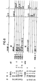
- T-states are defined in M286 with the most important actions listed in the description: TO, T1 and TL.
- the following T states are defined in M186 with the most important actions listed in the description: TO, T1, T2, T3 and TL.
- a so-called "Idle-STATE" (TI) is also defined jointly for M186 and M286, which is always present when none of the above-mentioned external activities T0, T1, T2. or T3 should take place.
- the present invention is based on the object of minimizing the requirements for the sequence control in an integrated micro-programmed device of the type mentioned at the beginning and in a method for its operation.
- the above-mentioned T-states can be meaningfully chained together and suitably overlapped, so that the above-mentioned bus cycle times of two T-states in M286 mode and of four T-states in M186 mode can be achieved.
- the machine control can be standardized so that it is possible to control the specific hardware complexes of the device according to the invention independently of, for example, the operating modes M186 and M286, so that they are compatible, for example, with the respective INTEL-BUS timing are.
- some ADMA-specific new T-states have been defined which can be overlaid with the above-mentioned T-states T0, T1, T2, T3, TL, TI according to certain criteria.
- the progressive T-States are generated by the "T-State Generator" TSG, which changes depending on the current T-State states and some parameters (IREADY, BIUSPLIT, IRESET, PRIOVLD, REQVLD, ORGMKWAIT, ISTE, RDWR and M186) always decides at the beginning of a phase PHI1 for a new T-state or for a combination of several T-states.
- T2 Second T-State of the M186-BUS cycle: Output of the external data on the 16-bit A / D-BUS in the event of a write access. Output of status information on the multiplexed address / status pins.
- T3 Third T-State of the M186-BUS cycle: Output of the external data on the 16-bit A / D-BUS in the event of a write access. Output of status information on the multiplexed address / status pins. Even with T3: Additional evaluation of a "READY" signal, which must be sent by a passive partner of the ADMA, at the beginning of T3; if this passive partner of the ADMA is not ready, a repetition of the T3 status is requested.
- the integrated high-performance DMA controller ADMA has four mutually independent channels that handle data transfer between media (storage, peripheral devices).
- the main control of the channels takes over micro programs.
- the sequence of the microinstructions is controlled by a sequencer SQ.
- the microprogram latch MLATCH contains the current microword necessary for processing a BUS cycle or for processing an internal organizational address calculation. A large number of the ADMA hardware units receive their instructions directly from the micro-program latch MLATCH.
- Each T-State extends over at least two phases PHI1 and PHI2.
- the task of the T-State T7B is to use phase PHI2 to read a 24-bit pointer address from the internal ADMA pointer register set.PR, to save it in an add latch ADD1 and to an address buffer at the "BUS INTERFACE UNIT "to transfer BIU. This 24 bit pointer address is used, among other things. later as an external address for an external read or write operation.
- T7B Another important task of T7B is to provide the following address of the current micro address in relation to the same channel. This task is carried out by the so-called "SEQUENZER" SQ, who decides on one of five different micro program address continuation options depending on a large number of parameters. See the parallel patent application "Device and method for subsequent address formation of a microprogram-controlled sequencer".
- the parameters from the command and status registers CR which are required for the generation of the microprogram subsequent address, are available towards the end of TVB PHI1.
- the microprogram sequence address for phase TVB PHI2 can be adopted in the so-called sequencer latch SLATCH.
- the sequencer latch SLATCH can be referred to as an internal ROM AdreB latch.
- the T-State TVE is usually the follow-up T-State of TVB if there was a valid microinstruction during TVB.
- the main task of the TVE is to provide the next microinstruction related to the channel that has just been processed. Therefore, during the TVE PHI1 phase, the internal microcode read-only memory ROM is read at the address transferred to the buffer SLATCH during the TVB PHI2 phase.
- the ROM output data stable at phase T7E PHI2 are written into the channel-specific microprogram instruction register MPIR if the microinstruction currently being processed is valid.
- the microprogram address in the SLATCH buffer is also transferred to the channel-specific microprogram address register MPAR.
- the further task of the TVE is to control an address pointer addition to phase PHI1.
- the first operand for this addition is the 24-bit pointer address stored in the adder buffer ADD1 during the TVB PHI2 phase.
- the second operand for this addition was, depending on the type of microinstruction, from the microword in the intermediate memory MLATCH via the OF line or by means of an autonomous one Offset logic is stored in a data handling unit DHU via line DO and also to phase TVB PHI2 in the adder buffer ADD2.
- a multiplexer MUX2 determines which operand is stored in the adder buffer ADD2.
- the result of the addition carried out in the adder ADD is written back into the 24-bit pointer register set PR at an address specified in the micro word if the microinstruction currently being processed is valid.
- T7E is additionally activated during the T-State in the event that the status for the start of an external read or write operation can be output on the external bus decremented channel-specific byte counter BC, and applied a clock pulse CL or read signal to the channel-specific data assembly register DAR of the autonomous data handling unit DHU.
- a hardware device which, regardless of the BUS width, for example 8 bit or 16 bit, enables the organization memory connected to the ADMA, in which the channel program of the ADMA is stored, and regardless of whether the command pointer address is even or odd, with just a single set of so-called "SETUP" microinstructions, the entire organizational transfers for loading the ADMA register CR, PR from the memory, which advantageously has a command block to reach.
- the word access request of the microprogram is converted into an actual byte access request by an autonomous unit, the BUS interface unit BIU.
- the external address is then incremented by 1 and a second byte access is again controlled independently, without requesting a new microinstruction.
- the marking of the T-states with TW serves to block the status evaluation of a match and verify unit during these split states and to inform the T-state generator TSG that two bus cycles must be carried out with one microinstruction .
- the data handling unit DHU has an offset control OC and an execution control EC. These controls OC, EC concern both the exchange of information with external information sources and with external information sinks.
- the 'micro word stored in the intermediate memory MLATCH supplies control signals SE for controlling the sequencer SQ and controls means PIP for pipelining data, controls the byte counter BC and supplies information for the address pointer control AC and for the sequencer control SQC and provides information for the control EWC des external write access.
- each pointer address can be incremented, decremented or kept constant.
- any physical BUS widths and logical BUS widths can be combined with one another.
- One channel can be prioritized using signals labeled PRIO in Fig. 1.
- the two signals PRIOVLD and REQVLD are shown combined in FIG. 1 as signals PRIO.
- the IRESET signal indicates that there is an internal reset.
- the two phases PHI1 and PHI2 are controlled by a clock generator, which in turn is controlled by the clock signal CL.
- the addition "-Q" after a signal designation means that the signal designated thereby is in inverted form. All T-States are evaluated by the ADMA during the PHI1 phase. If a T-State for phase PHI2 is still required, it must be temporarily stored in a latch with phase PHI1 with a transfer gate at the respective unit where it is required.
- Fig. 3 shows an M286 ADMA timing diagram. Data should be read from a data source.
- the microprogram instruction register MPIR of the prioritized channel is selected in the ADMA and transferred to a microprogram latch MLATCH.
- the channel-specific subsequent micro address is generated in the sequencer by incrementing the previous micro address via the signal SI. As long as the selected microinstruction from the register MPIR is valid, the signal MPIRS is active.
- the external address is read out from the internal ADMA pointer register set PR via the activated signal AREG, where the data are to be read out. At the same time, this external address is stored in the adder buffer ADD1 and transferred to an address buffer in the BUS interface unit BIU.
- the T-State TI was given simultaneously with T7B.
- a new external address is generated in adder ADD and written back to address register AREG during TVE PHI2.
- the internal microcode read-only memory ROM is read.
- the ROM output data stable at phase T7E PHI2 are written into the channel-specific register MPIR when the microinstruction currently being processed is valid.
- the associated microprogram address is also transferred to the channel-specific microprogram address register MPAR.
- TO is available for the currently valid microinstruction:
- the external address EA is active.
- the external data ED are taken over by the ADMA.
- Fig. 4 shows an M186 ADMA timing diagram.
- the timing diagram of Figure 4 also describes reading data from an external data source. Differences between the diagrams of Fig. 3 and Fig. 4 result exclusively from differences between the modes M186 and M286.
- the M186 has two additional T-states, namely T2 and T3. Status information is essentially output during T2 and T3. Towards the end of T3, the external data ED are taken over by the ADMA.
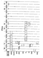
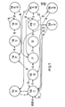
- T-state diagram for BUS cycles in M186 mode and M286 mode shows a T-state diagram for BUS cycles in M186 mode and M286 mode. It can be seen that in both modes the T-State TL of a BUS cycle basically overlaps with the T-State TO of the immediately following BUS cycle. This makes it possible to achieve bus cycle times of two T-states in the M286 mode and BUS cycle times of four T-states in the M186 mode. If there is no valid selection MPIRS of a microinstruction register MPIR during TO of a BUS cycle, TL of such a BUS cycle overlaps with TI. This state TI then continues until there is a valid selection MPIRS of a microinstruction register MPIR (see also FIGS. 3 and 4). 5 shows the overlap of a first bus cycle B1 with a second bus cycle B2 and a third bus cycle B3 as a function of time t.
- Fig. 6 shows an M286 mode ADMA state diagram.
- Fig. 7 shows an M186 mode ADMA state diagram.
- These state diagrams have large circles between which transitions labeled with numbers are possible.
- Each large circle represents a state which is characterized by an overlap of the T-states specified in the large circle in question.
- the T-states indicated in a large circle are to be understood such that during the state represented by this large circle, the T-states entered in this large circle are active and the T-states not shown in this large circle are inactive.
- the transition from one large circle to another large circle occurs depending on which T-states are active in the first large group and which parameters are available on the T-state generator TSG. Differences between the diagrams of Fig. 6 and of Fig. 7 again only result from differences between the M186 mode and the M286 mode.
- An arrow pointing up means the logical link "AND”.
- a "V" represents the logical link "OR”.
- the numbers of the two transitions in Fig. 8 correspond to the numbers in the small circles at the transitions in Figs. 6 and 7.
- the designation for the numbers of the transitions in Fig. 8 is U: M186 for transitions in the M186 diagram and U: M286 for transitions in M286 mode state diagram.
- Line 20 means that the next T-State becomes the T-State TVE if the following parameters currently apply: TVB active and TI active and TL inactive and PRIOVLD active.
- the associated transitions can be observed in the diagrams of Fig. 6 and Fig. 7 under transition numbers 3, 5. These transitions 3, 5 can then also be separated by asking under which conditions BE is the next T-state the T-state TO or alternatively the T-state TI.
- All input parameters to the T-state generator TSG (these input parameters do not include the signals CL, PHI1, PHI2), which are not explicitly mentioned in the respective line from line 01 to line 48 in column 8 in FIG respective relevant transition from one state to the next state is inactive.
- T-state generator TSG can be implemented as a synchronous switching mechanism as a "programmable logic array" (PLA) with a regular structure.
- PPA programmable logic array
- a specialist only needs the knowledge from the textbook by C. Mead and L. Conway: “Introduction to VLSI Systems", Addison-Wesley, chapter 3.10 "The programmable logic array” and the truth table from Fig. 8 and the knowledge of Block diagram of the T-state generator TSG from Fig. 2, in order to be able to immediately specify the switching mechanism for the T-state generator TSG.
- the output signals of the T-state generator TSG can be buffered in a flip-flop row with clocked R, S flip-flops.
- the first microinstruction is in the reading phase
- the second microinstruction is in the execution phase (e.g. output) external address)
- the third microinstruction is in the sequencing, reading from ROM, predecoding.
- a channel change must be possible after each command execution. Because of the high performance requirements, such a switchover from one channel to the other takes place without influencing the pipeline chain (PIP).
- PIP pipeline chain
- This can e.g. mean that a command for channel 2 is read from the ROM and pre-decoded, but that the command is subsequently executed for a command from channel 1, while at the same time a reading phase is being processed for channel 2.
- the execution phase (minimum command time) lasts 250 ns.
- the register CR comprises channel-specific control registers.
- the PR register contains the addresses of the data source and data sink. There is also a byte counter register that specifies how many bytes are captured by a data transfer. All these registers are loaded during a 'SETUP' of the ADMA.
Landscapes
- Engineering & Computer Science (AREA)
- Theoretical Computer Science (AREA)
- Physics & Mathematics (AREA)
- General Engineering & Computer Science (AREA)
- General Physics & Mathematics (AREA)
- Bus Control (AREA)
- Executing Machine-Instructions (AREA)
- Debugging And Monitoring (AREA)
- Electrotherapy Devices (AREA)
Applications Claiming Priority (2)
| Application Number | Priority Date | Filing Date | Title |
|---|---|---|---|
| DE19823241378 DE3241378A1 (de) | 1982-11-09 | 1982-11-09 | Integrierte mikroprogrammierte vorrichtung zur steuerung von informationsverarbeitungsablaeufen und verfahren zu ihrem betrieb |
| DE3241378 | 1982-11-09 |
Publications (3)
| Publication Number | Publication Date |
|---|---|
| EP0108415A2 true EP0108415A2 (fr) | 1984-05-16 |
| EP0108415A3 EP0108415A3 (en) | 1986-12-10 |
| EP0108415B1 EP0108415B1 (fr) | 1995-01-25 |
Family
ID=6177661
Family Applications (1)
| Application Number | Title | Priority Date | Filing Date |
|---|---|---|---|
| EP83111100A Expired - Lifetime EP0108415B1 (fr) | 1982-11-09 | 1983-11-07 | Dispositif intégré et microprogrammé pour la commande du déroulement de traitement d'informations et procédé pour sa mise en oeuvre |
Country Status (5)
| Country | Link |
|---|---|
| US (1) | US4600991A (fr) |
| EP (1) | EP0108415B1 (fr) |
| JP (1) | JPS5999547A (fr) |
| AT (1) | ATE117816T1 (fr) |
| DE (2) | DE3241378A1 (fr) |
Cited By (3)
| Publication number | Priority date | Publication date | Assignee | Title |
|---|---|---|---|---|
| EP0185260A3 (en) * | 1984-12-14 | 1988-10-05 | Alcatel N.V. | Interface for direct information transfer |
| EP0328450A3 (fr) * | 1988-02-08 | 1991-10-16 | Fujitsu Limited | Dispositif de commande d'accès direct de mémoire |
| EP0336756A3 (fr) * | 1988-04-08 | 1992-10-21 | Fujitsu Limited | Dispositif de commande d'accès direct de mémoire |
Families Citing this family (1)
| Publication number | Priority date | Publication date | Assignee | Title |
|---|---|---|---|---|
| US7870444B2 (en) * | 2005-10-13 | 2011-01-11 | Avago Technologies Fiber Ip (Singapore) Pte. Ltd. | System and method for measuring and correcting data lane skews |
Family Cites Families (1)
| Publication number | Priority date | Publication date | Assignee | Title |
|---|---|---|---|---|
| US4112490A (en) * | 1976-11-24 | 1978-09-05 | Intel Corporation | Data transfer control apparatus and method |
-
1982
- 1982-11-09 DE DE19823241378 patent/DE3241378A1/de not_active Withdrawn
-
1983
- 1983-11-07 AT AT83111100T patent/ATE117816T1/de not_active IP Right Cessation
- 1983-11-07 DE DE3382778T patent/DE3382778D1/de not_active Expired - Lifetime
- 1983-11-07 US US06/549,583 patent/US4600991A/en not_active Expired - Lifetime
- 1983-11-07 EP EP83111100A patent/EP0108415B1/fr not_active Expired - Lifetime
- 1983-11-08 JP JP58209751A patent/JPS5999547A/ja active Pending
Non-Patent Citations (3)
| Title |
|---|
| ELECTRONIC DESIGN, vol. 27, no. 7, 29 March 1979 (1979-03-29), pages 102 - 106 |
| ELECTRONIC LETTERS, vol. 17, no. 19, 17 September 1981 (1981-09-17), pages 709 - 710 |
| IBM TECHNICAL DISCLOSURE BULLETIN, vol. 20, no. 4, September 1977 (1977-09-01), pages 1524 - 1525 |
Cited By (3)
| Publication number | Priority date | Publication date | Assignee | Title |
|---|---|---|---|---|
| EP0185260A3 (en) * | 1984-12-14 | 1988-10-05 | Alcatel N.V. | Interface for direct information transfer |
| EP0328450A3 (fr) * | 1988-02-08 | 1991-10-16 | Fujitsu Limited | Dispositif de commande d'accès direct de mémoire |
| EP0336756A3 (fr) * | 1988-04-08 | 1992-10-21 | Fujitsu Limited | Dispositif de commande d'accès direct de mémoire |
Also Published As
| Publication number | Publication date |
|---|---|
| ATE117816T1 (de) | 1995-02-15 |
| DE3241378A1 (de) | 1984-05-10 |
| JPS5999547A (ja) | 1984-06-08 |
| EP0108415A3 (en) | 1986-12-10 |
| DE3382778D1 (de) | 1995-03-09 |
| EP0108415B1 (fr) | 1995-01-25 |
| US4600991A (en) | 1986-07-15 |
Similar Documents
| Publication | Publication Date | Title |
|---|---|---|
| DE2411963C3 (de) | Elektronische Datenverarbeitungsanlage mit einer Prioritätssteuerschaltung mit änderbaren Steuerblöcken | |
| DE2251876C3 (de) | Elektronische Datenverarbeitungsanlage | |
| DE69906156T2 (de) | Mikroprozessorvorrichtung mit programmierbaren wartezuständen | |
| DE3752017T2 (de) | Mikrorechner mit Zugriffsfähigkeit auf einen internen Speicher mit gewünschter variabler Zugriffszeit | |
| DE68920929T2 (de) | Zeitgeberkanal mit mehreren Zeitgeberreferenzmerkmalen. | |
| DE2953861C2 (fr) | ||
| DE1774296B2 (de) | Restruktuierbare Steuereinheit für elektronische Digitalrechner | |
| DE68915074T2 (de) | Integrierte Zeitgeberschaltung mit mehreren Kanälen und zugeordnetem Bedienungsprozessor. | |
| DE68924810T2 (de) | Zeitgeberkanal für die Verwendung in einem Mehrkanal-Zeitsystem. | |
| DE2755616A1 (de) | Asymmetrischer multiprozessor | |
| DE68919018T2 (de) | Zeitgeberkanal mit Übereinstimmungserkennungsmerkmalen. | |
| DE3587446T2 (de) | Signalverarbeitungsprozessor und hierarchische Multiverarbeitungstruktur mit mindestens einem solchen Prozessor. | |
| DE3114921A1 (de) | Datenverarbeitungssystem | |
| DE69032511T2 (de) | Multiprozessor-Steuereinrichtung mit gemeinsamem Steuerungsspeicher | |
| DE3882425T2 (de) | Datenübertragungssteuerungsvorrichtung für Direktspeicherzugriff. | |
| DE4022365C2 (de) | Datenübertragungssystem | |
| EP0130269A2 (fr) | Commande à programme mémorisé | |
| EP0108415B1 (fr) | Dispositif intégré et microprogrammé pour la commande du déroulement de traitement d'informations et procédé pour sa mise en oeuvre | |
| DE69528824T2 (de) | Apparat und verfahren zum erneuern von informationen in einem beschreibbaren mikrokode-kontrollspeicher | |
| EP0111161B1 (fr) | Dispositif pour la préparation de micro-instructions pour au moins deux unités fonctionnelles qui fonctionnent indépendamment dans un module électronique intégré et microprogrammé et procédé pour sa mise en oeuvre | |
| DE2847479A1 (de) | Schablonenfamilien-schnittstelleneinrichtung | |
| DE2717700A1 (de) | Speicherzugriffsanordnung | |
| EP0108418B1 (fr) | Dispositif pour la commande microprogrammée d'un transfert d'informations et procédé pour sa mise en oeuvre | |
| DE69327043T2 (de) | Datenverarbeitungsvorrichtung | |
| DE3687739T2 (de) | Speicheranordnung mit mehrfachem lese-schreibzugriff. |
Legal Events
| Date | Code | Title | Description |
|---|---|---|---|
| PUAI | Public reference made under article 153(3) epc to a published international application that has entered the european phase |
Free format text: ORIGINAL CODE: 0009012 |
|
| AK | Designated contracting states |
Designated state(s): AT DE FR GB IT |
|
| 17P | Request for examination filed |
Effective date: 19841214 |
|
| PUAL | Search report despatched |
Free format text: ORIGINAL CODE: 0009013 |
|
| AK | Designated contracting states |
Kind code of ref document: A3 Designated state(s): AT DE FR GB IT |
|
| 17Q | First examination report despatched |
Effective date: 19880128 |
|
| GRAA | (expected) grant |
Free format text: ORIGINAL CODE: 0009210 |
|
| AK | Designated contracting states |
Kind code of ref document: B1 Designated state(s): AT DE FR GB IT |
|
| REF | Corresponds to: |
Ref document number: 117816 Country of ref document: AT Date of ref document: 19950215 Kind code of ref document: T |
|
| REF | Corresponds to: |
Ref document number: 3382778 Country of ref document: DE Date of ref document: 19950309 |
|
| ITF | It: translation for a ep patent filed | ||
| GBT | Gb: translation of ep patent filed (gb section 77(6)(a)/1977) |
Effective date: 19950407 |
|
| ET | Fr: translation filed | ||
| PLBE | No opposition filed within time limit |
Free format text: ORIGINAL CODE: 0009261 |
|
| STAA | Information on the status of an ep patent application or granted ep patent |
Free format text: STATUS: NO OPPOSITION FILED WITHIN TIME LIMIT |
|
| 26N | No opposition filed | ||
| PGFP | Annual fee paid to national office [announced via postgrant information from national office to epo] |
Ref country code: AT Payment date: 19981021 Year of fee payment: 16 |
|
| PG25 | Lapsed in a contracting state [announced via postgrant information from national office to epo] |
Ref country code: AT Free format text: LAPSE BECAUSE OF NON-PAYMENT OF DUE FEES Effective date: 19991107 |
|
| REG | Reference to a national code |
Ref country code: GB Ref legal event code: IF02 |
|
| PGFP | Annual fee paid to national office [announced via postgrant information from national office to epo] |
Ref country code: GB Payment date: 20021107 Year of fee payment: 20 |
|
| PGFP | Annual fee paid to national office [announced via postgrant information from national office to epo] |
Ref country code: FR Payment date: 20021129 Year of fee payment: 20 |
|
| PGFP | Annual fee paid to national office [announced via postgrant information from national office to epo] |
Ref country code: DE Payment date: 20030121 Year of fee payment: 20 |
|
| PG25 | Lapsed in a contracting state [announced via postgrant information from national office to epo] |
Ref country code: GB Free format text: LAPSE BECAUSE OF EXPIRATION OF PROTECTION Effective date: 20031106 |
|
| REG | Reference to a national code |
Ref country code: GB Ref legal event code: PE20 |
|
| APAH | Appeal reference modified |
Free format text: ORIGINAL CODE: EPIDOSCREFNO |