EP0108417A2 - Méthode pour commander le transfert de données entre un transmetteur de données et un récepteur de données sur un bus, au moyen d'une unité de commande connectée au bus - Google Patents
Méthode pour commander le transfert de données entre un transmetteur de données et un récepteur de données sur un bus, au moyen d'une unité de commande connectée au bus Download PDFInfo
- Publication number
- EP0108417A2 EP0108417A2 EP83111102A EP83111102A EP0108417A2 EP 0108417 A2 EP0108417 A2 EP 0108417A2 EP 83111102 A EP83111102 A EP 83111102A EP 83111102 A EP83111102 A EP 83111102A EP 0108417 A2 EP0108417 A2 EP 0108417A2
- Authority
- EP
- European Patent Office
- Prior art keywords
- data
- transfer
- address
- control device
- command
- Prior art date
- Legal status (The legal status is an assumption and is not a legal conclusion. Google has not performed a legal analysis and makes no representation as to the accuracy of the status listed.)
- Granted
Links
Images


Classifications
-
- G—PHYSICS
- G06—COMPUTING OR CALCULATING; COUNTING
- G06F—ELECTRIC DIGITAL DATA PROCESSING
- G06F13/00—Interconnection of, or transfer of information or other signals between, memories, input/output devices or central processing units
- G06F13/14—Handling requests for interconnection or transfer
- G06F13/20—Handling requests for interconnection or transfer for access to input/output bus
- G06F13/28—Handling requests for interconnection or transfer for access to input/output bus using burst mode transfer, e.g. direct memory access DMA, cycle steal
- G06F13/285—Halt processor DMA
Definitions
- the invention relates to a method for controlling the data transfer between a data transmitter and a data receiver via a bus with the aid of a control device connected to the bus, which controls the data transfer between the data transmitter and the data receiver as a function of a channel program containing transfer commands and control commands in such a way that causes by means of a transfer command in a first cycle, the data are transferred to a buffer memory of the control device and in a second cycle from the buffer memory to the data receiver, and in which the assigned transfer command in each case contains a mode coding for handling the data transmitter address and the data receiver address.
- a data transmitter for example a memory
- a data receiver for example a peripheral device
- the memory and the D eripheren devices are connected to a bus, in which an address bus, a data bus and a control bus are summarized.
- the control of the data transfer between the data transmitter and the data receiver is carried out as a function of a channel program, in which transfer commands and control commands are contained, with the aid of a control device connected to the bus.
- a channel command with which a data transfer is carried out usually contains the channel command word which describes the operation to be performed and various parameters, such as the number of bytes to be transferred, the address of the data sender and the address of the data receiver.
- channel commands can be linked to a channel program by so-called command chaining.
- control commands that perform organizational tasks.
- the data transfer can be carried out in two cycles. In a first cycle, the data are transferred from the data transmitter into a buffer memory of the control device, in a second cycle, the data are then transferred from the buffer memory of the control device to the data receiver.
- the control device e.g. the DMA control
- data transfer in two cycles is unfavorable if data from the data transmitter is only to be transferred to the control device or data from the control device is only to be transferred to the gene data receiver.
- Such operations occur very frequently, for example when the device status register of a peripheral device is to be read or a read command is to be written into a device command register etc. In such operas A data transfer is also carried out, but this data transfer is used for control purposes.
- the transfer commands mentioned above can also be used to transmit data only from the data transmitter to the control device or from the control device to the data receiver. Then, however, would have to read a register in the data receiver, a memory cell will be indicated in the data transmitter, although the date is required only in the control device, the data receiver has no use for the date '.
- the object on which the invention is based is to modify a method for controlling the data transfer between a data transmitter and a data receiver via a bus with the aid of a control device connected to the bus in such a way that the transfer commands available for the data transfer between the data transmitter and the data receiver also for the transfer of Data from the data transmitter to the control device or control device to the data receiver can be used without the unnecessary second cycle of data transmission being necessary.
- This object is achieved in a method of the type mentioned at the outset in that, in order to implement an exclusive data transfer from the data transmitter to the control device, the transfer command contains such a mode coding for the data receiver address that the control device only initiates the data transmission between the data transmitter and the buffer memory of the control device.
- the object is achieved in a method of the type mentioned in the introduction that in order to implement an exclusive data transfer from the control device to the data receiver, the transfer command contains such a mode coding for the data sender address that the control device only transfers data between rule the buffer memory of the control device and the data receiver.
- the channel command is a transfer command
- the data send. address, the data recipient address and the number of data to be transmitted it is useful to replace the data sending address with the date to be transmitted, which is then transmitted to the data recipient.
- control device is a DMA controller which contains a microprogram memory addressed by a sequencer for recording the microprograms assigned to the channel commands, an address unit for recording the data receiver and data transmission addresses, a data level with the buffer memory, a control register level and a data counter.
- the channel command can then be stored in a channel command register contained in the control register stage, which is connected to the sequencer, which addresses a microprogram associated with the channel command in the microprogram memory.
- the addressing unit is controlled by the microinstructions in such a way that it sends the address of the date to be transmitted in the data transmitter via the bus to the data transmitter, which then transfers the date to the data stage, specifically into the buffer memory. wearing.
- the data is also transmitted from the control device to the data receiver.
- the microcomputer system shown in Figure 1 consists of a microprocessor MP, e.g. an IAPX 80286 from Intel, a peripheral device PG, a memory MM and a control device DMA. These units are all connected to one another via a bus BU, in which an address bus AB, a data bus DB and a control bus SB are combined. If a data transfer between the data transmitter, e.g. the memory MM, and the data receiver, e.g. the peripheral device PG, the microprocessor MC issues a channel start command to the control device DMA. The control device DMA then takes over control of the data transfer between the memory MM and the peripheral device PG, the bus allocation being controlled by the MC via the HOLD / HLDA sequences.
- a microprocessor MP e.g. an IAPX 80286 from Intel
- a peripheral device PG e.g. an IAPX 80286 from Intel
- a peripheral device PG e.g. an IAPX 80
- the microprocessor MC is thus relieved of the data transfer and can perform other tasks.
- the control device DMA issues an interrupt request IT to the microprocessor MC and informs the microprocessor MC of the end of the data transfer.
- the data transfer from the data transmitter to the data receiver takes place as a function of a channel program which contains transfer commands for controlling the data transfer and control commands for executing organizational operations.
- the channel programs are stored, for example, in the memory MM and are stored there by the microprocessor MC.
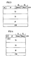
- the structure of such a channel command is shown in FIG. 3.
- the channel command consists of the channel command word CCW, the data transmitter address SA, the data receiver address DA, the number of bytes BY to be transmitted and the channel status word CSW.
- the channel command word CCW contains various components.
- the first component DY specifies whether a transfer command or a control command is carried out.
- the operation code OP is specified, in a third part DE there are details of how the data receiver address is to be modified (mode), whether a byte or a data word is to be transmitted and in which direction the data transmission should take place.
- the component SO specifies how the data sender address is to be modified, whether bytes or data words are to be transmitted in each case and which direction the data transmission is taking.
- the control device can thus determine whether a transfer command should be carried out and, if so, what address the data transmitter has and what address the data receiver has.
- the control device can determine the number of bytes to be transmitted, whether a word or a byte is to be transmitted in each case and whether the data transmission is to take place from the memory to the peripheral device or from the peripheral device to the memory.
- the control device can determine whether the address of the data receiver or data transmitter remains unchanged after the transfer has been carried out or has to be incremented or decremented.
- the data transfer between the data transmitter and the data receiver takes place in two cycles.
- the data from the data transmitter are transferred to a buffer memory of the control device DMA
- the second cycle the data are transferred from the buffer memory of the control device DMA to the data receiver.
- the channel command is changed.
- the mode part of the component DE of the channel command word is provided with a specific coding, for example 11, while the mode part of the component SO of the channel command word retains its normal meaning.
- the address SA of the data transmitter is also specified in the channel command, while the address DA of the data receiver is no longer important and can be omitted. If the component DE of the channel command word CCW has the specified coding, then the control device DMA only carries out the first cycle of the data transfer, but suppresses the second cycle. The control device DMA can then check and evaluate the date contained in the buffer memory.
- the channel command is changed in accordance with FIG. 4.
- the component SO of the channel command word CCW now receives the specified mode coding, while the component DE retains the usual form.
- the address DA of the data receiver is specified in the channel command, while the address SA of the data transmitter is replaced by a selectable data word. This data word is then transmitted from the control device DMA to the data receiver.
- data transmission is only carried out in one cycle, the other cycle is suppressed.
- the content of the channel command part BY can be set to 1 or omitted entirely.
- the component SO of the channel command word would have to.
- CCW have the mode coding 11.
- the pattern to be transferred would have to be specified in component SA of the command word.
- the component BY of the channel command should contain a corresponding value and the component DE of the channel command word CCW should have the mode coding 11.
- the address of the magnetic tape would be given as the address SA of the data transmitter.
- FIG. 2 shows the structure of a control device which is implemented as a DMA controller.
- the DMA controller contains a sequencer SE of known construction (cf. reference given above) consisting of a condition multiplexer CC, a command decoder MAP, a first multiplexer MUX1, a microinstruction address register MA, a command adder AD1 and a second multiplexer MUX2.
- a micro program memory; MPS is connected to the sequencer SE, in which the micro programs assigned to the channel commands are stored. If a channel command is to be carried out, the command decoder MAP addresses the microprogram assigned in the microprogram memory MPS and the microprogram memory. MPS issued the corresponding microinstructions.
- microinstructions are stored in a microinstruction register MBR, from which the control signals are then sent to the other units of the control device.
- Sequencer SE Sequencer SE
- micro program memory MPS micro instruction register MBR
- micro instruction register MBR The interaction of Sequencer SE, micro program memory MPS and micro instruction register MBR is known and can e.g. can be found in the above-mentioned literature.
- the microinstruction register MBR is connected directly or via an internal address and control bus IA to an address unit AU in which the address of the channel command to be executed is stored and in which the address of the channel command is modified in accordance with the information in the channel command word CCW.
- the address unit AU contains an address register ADR for receiving the address of the channel command, an adder AD for calculating the new address of the channel command and a buffer memory rS1 for temporarily storing the address before it is sent to the address bus AB.
- To calculate the new address of the channel command word in the adder AD it can be supplied with a corresponding size via a multiplexer MUX3. This can be taken from the microinstruction register MBR or set by a register RG1.
- the DMA controller also contains a data stage DU, in which the buffer memory DAR is contained.
- the data stage DU is connected to the data bus DB, specifically to a buffer PS2.
- An input register EPS is arranged between the intermediate memory PS2 and the input of the buffer memory DAR, and an output register APS is arranged between the output of the buffer memory DAR and the intermediate memory PS2.
- the buffer memory DAR is also connected to the internal bus IA for the addresses and control signals and an internal bus ID for the data.
- a switch S1 is arranged in the data stage DU, with which the addresses coming from the microprocessor MC can be switched through from the address unit AU to the internal address bus IA (for addressing an internal register).
- the number of bytes to be transferred per data transfer is determined using a byte counter BZ, which is connected to the internal buses ID and IA.
- control registers CR are also provided. To include the channel status register CSR, the command register GCR and in particular the channel command register CCR. These control registers CR are connected in particular to the sequencer SE, in the manner shown in FIG. 2.
- No further units of the DMA controller are required to explain the method according to the invention. These include e.g. a clock generator TG and an adaptation circuit ANS, which establishes the connection to the microprocessor MC. Furthermore, a priority circuit PR can be provided, which selects the unit with the highest priority when there are operating requests from several data transmitters or data receivers. With the aid of a circuit arrangement ITS for generating an interrupt request IT, the microprocessor MC can be informed when the channel program has been ended by the DMA controller.
- the microprocessor MC first loads the channel programs into the memory MM. It also loads the address register ADR with the address of the first channel command to be processed in the channel program and the command register GCR with the start command. The DMA controller then takes over the further processing of the channel program. From the command register GCR, which is connected to the sequencer SE, the micro-program required for the command initiation is addressed in the micro-program memory MPS via the command decoder MAP. The first channel / command is transferred to the channel command register CCR with the aid of the assigned microinstructions which are transmitted to the microinstruction register MBR. It follows whether the channel command is a transfer command as shown in FIG. 3.
- the sequencer SE which is connected to the channel command register CCR, determines whether the mode coding in component DE or SO of channel command word CCW is binary 11 or not. Furthermore, the sequencer SE, by controlling the corresponding microprograms in the microprogram memory MPS, causes the byte counter BZ to be loaded with the number of bytes to be transmitted and for the address of the data transmitter or the address of the data receiver to be loaded into the address register ADR.
- the corresponding addresses are in: K anal command ( Figure 3) included.
- the Sequencer SE determines by evaluating the channel command that e.g. a channel command corresponding to Figure 4 is present, then it addresses the assigned microprogram in the microprogram memory MPS, which causes the content SA of the channel command to be transferred from the buffer memory DAR via the register APS and the buffer memory PS2 to the data bus DB. From the contents of the byte counter BZ it can be seen whether this process has to be carried out once or several times.
- the sequencer SE determines that the mode part of the command part DE is binary 11 in the channel command word CCW, then it addresses the microprogram in the microprogram memory MPS, which causes the data transmission from the data transmitter to the 'buffer memory DAR, but suppresses the further transmission to the data receiver.
- the transmission can take place several times, according to the content of the byte counter BZ.
- the channel status register CSR is set in accordance with the cause of the termination and the content of the channel status register CSR is transferred to the memory MM, specifically to the component CSW of the channel command.
- the mode of operation of the SE sequencer can be found in the literature reference given above.
- the start address of the Microprograms in the microprogram memory MPS are in each case taken by the command decoder MAP from the channel command in the channel command register CCR or from the start command in the command register GCR.
- the further addresses of the microinstructions are determined with the aid of the adder DR or obtained from the previous microinstruction via the microinstruction register MBR.
Landscapes
- Engineering & Computer Science (AREA)
- Theoretical Computer Science (AREA)
- Physics & Mathematics (AREA)
- General Engineering & Computer Science (AREA)
- General Physics & Mathematics (AREA)
- Bus Control (AREA)
- Communication Control (AREA)
- Information Transfer Systems (AREA)
Priority Applications (1)
| Application Number | Priority Date | Filing Date | Title |
|---|---|---|---|
| AT83111102T ATE45434T1 (de) | 1982-11-09 | 1983-11-07 | Verfahren zum steuern des datentransfers zwischen einem datensender und einem datenempfaenger ueber einen bus mit hilfe einer am bus angeschlossenen steuereinrichtung. |
Applications Claiming Priority (2)
| Application Number | Priority Date | Filing Date | Title |
|---|---|---|---|
| DE3241359 | 1982-11-09 | ||
| DE19823241359 DE3241359A1 (de) | 1982-11-09 | 1982-11-09 | Verfahren zum steuern des datentransfers zwischen einem datensender und einem datenempfaenger ueber einen bus mit hilfe einer am bus angeschlossenen steuereinrichtung |
Publications (3)
| Publication Number | Publication Date |
|---|---|
| EP0108417A2 true EP0108417A2 (fr) | 1984-05-16 |
| EP0108417A3 EP0108417A3 (en) | 1986-12-30 |
| EP0108417B1 EP0108417B1 (fr) | 1989-08-09 |
Family
ID=6177652
Family Applications (1)
| Application Number | Title | Priority Date | Filing Date |
|---|---|---|---|
| EP83111102A Expired EP0108417B1 (fr) | 1982-11-09 | 1983-11-07 | Méthode pour commander le transfert de données entre un transmetteur de données et un récepteur de données sur un bus, au moyen d'une unité de commande connectée au bus |
Country Status (4)
| Country | Link |
|---|---|
| EP (1) | EP0108417B1 (fr) |
| JP (1) | JPS5999528A (fr) |
| AT (1) | ATE45434T1 (fr) |
| DE (2) | DE3241359A1 (fr) |
Cited By (1)
| Publication number | Priority date | Publication date | Assignee | Title |
|---|---|---|---|---|
| CN100481049C (zh) * | 2005-11-10 | 2009-04-22 | 威盛电子股份有限公司 | 数据储存与传送方法 |
Family Cites Families (2)
| Publication number | Priority date | Publication date | Assignee | Title |
|---|---|---|---|---|
| US4246637A (en) * | 1978-06-26 | 1981-01-20 | International Business Machines Corporation | Data processor input/output controller |
| JPS5789128A (en) * | 1980-11-25 | 1982-06-03 | Hitachi Ltd | Controlling system for information interchange |
-
1982
- 1982-11-09 DE DE19823241359 patent/DE3241359A1/de not_active Withdrawn
-
1983
- 1983-11-07 DE DE8383111102T patent/DE3380372D1/de not_active Expired
- 1983-11-07 EP EP83111102A patent/EP0108417B1/fr not_active Expired
- 1983-11-07 AT AT83111102T patent/ATE45434T1/de not_active IP Right Cessation
- 1983-11-07 JP JP58208897A patent/JPS5999528A/ja active Pending
Cited By (1)
| Publication number | Priority date | Publication date | Assignee | Title |
|---|---|---|---|---|
| CN100481049C (zh) * | 2005-11-10 | 2009-04-22 | 威盛电子股份有限公司 | 数据储存与传送方法 |
Also Published As
| Publication number | Publication date |
|---|---|
| ATE45434T1 (de) | 1989-08-15 |
| EP0108417B1 (fr) | 1989-08-09 |
| EP0108417A3 (en) | 1986-12-30 |
| JPS5999528A (ja) | 1984-06-08 |
| DE3241359A1 (de) | 1984-05-10 |
| DE3380372D1 (en) | 1989-09-14 |
Similar Documents
| Publication | Publication Date | Title |
|---|---|---|
| EP0108969B1 (fr) | Unité de commande DMA pour la transmission des données entre un transmetteur de données et un récepteur de données | |
| DE2744531C2 (de) | Anordnung zur Auswahl von Unterbrechnungsprogrammen in einer Datenverarbeitungsanlage | |
| EP0006164B1 (fr) | Système multiprocesseur avec mémoires utilisables en commun | |
| EP0193104A2 (fr) | Commande de transfert de données | |
| DE2411963A1 (de) | Datenverarbeitungsanlage | |
| DE69028836T2 (de) | Datenverarbeitungssystem mit Direktspeicherzugriffssteuerung und Verfahren zur Busmasteränderung unter Verwendung Unterbrechungen mit gegebener Priorität | |
| DE2911909C2 (de) | Digitales Datenverarbeitungsgerät | |
| EP0110199B1 (fr) | Méthode pour commander le transfert de données entre un transmetteur de données et un récepteur de données sur un bus, au moyen d'une unité de commande connectée au bus | |
| DE1549474A1 (de) | Einrichtung zur Ausfuehrung von Operationen in elektronischen Datenverarbeitungsanlagen | |
| DE3587874T2 (de) | Protokolle für Terminal. | |
| EP0108417B1 (fr) | Méthode pour commander le transfert de données entre un transmetteur de données et un récepteur de données sur un bus, au moyen d'une unité de commande connectée au bus | |
| EP0895168B1 (fr) | Système de communication avec une interface sérielle | |
| EP0108413B1 (fr) | Méthode pour commander le transfert de données entre un transmetteur de données et un récepteur de données sur un bus, au moyen d'une unité de commande connectée au bus | |
| DE2606295C3 (de) | Anordnung zur Übertragung von Zeichen zwischen über einen Multiplexkanal ansteuerbaren peripheren Einheiten und einem Arbeitsspeicher eines Zentralprozessors | |
| DE69417123T2 (de) | Datenverarbeitungssystem mit serieller Schnittstelle | |
| EP0108418B1 (fr) | Dispositif pour la commande microprogrammée d'un transfert d'informations et procédé pour sa mise en oeuvre | |
| DE2856768C2 (de) | Prioritäts-Vektor-Unterbrechungsvorrichtung | |
| DE3129560C2 (de) | Steuerschaltung für einen Drucker | |
| EP0566985B1 (fr) | Méthode et dispositif de transmission de paquets de données | |
| EP0297480B1 (fr) | Méthode et dispositif de régulation de la charge d'un système de lignes de données pour dispositifs entrée/sortie dans une installation de traitement de données | |
| DE2430693A1 (de) | Schnittstellenschaltung fuer den anschluss einer satelliten-datenverarbeitungsanlage an einen datenuebertragungskanal | |
| EP0108416B1 (fr) | Dispositif pour la commande de lancement d'un canal dans un dispositif intégré microprogrammé avec au moins deux canaux indépendants pour la manipulation d'informations et procédé pour sa mise en oeuvre | |
| DE10029024A1 (de) | Direktspeicherzugriffssteuereinheit | |
| EP0167125B1 (fr) | Méthode et circuit pour la détermination statistique des commandes opérationnelles de commutation actives dans un central de télécommunication | |
| EP0339466B1 (fr) | Méthode et dispositif pour la préparation en temps réel des mots du canal de commande sans lecture anticipée par l'exécution d'une opération d'entrée-sortie d'un système d'entrée-sortie travaillant avec des adresses réelles d'un dispositif de traitement de données |
Legal Events
| Date | Code | Title | Description |
|---|---|---|---|
| PUAI | Public reference made under article 153(3) epc to a published international application that has entered the european phase |
Free format text: ORIGINAL CODE: 0009012 |
|
| AK | Designated contracting states |
Designated state(s): AT DE FR GB IT |
|
| 17P | Request for examination filed |
Effective date: 19841214 |
|
| PUAL | Search report despatched |
Free format text: ORIGINAL CODE: 0009013 |
|
| AK | Designated contracting states |
Kind code of ref document: A3 Designated state(s): AT DE FR GB IT |
|
| 17Q | First examination report despatched |
Effective date: 19871229 |
|
| GRAA | (expected) grant |
Free format text: ORIGINAL CODE: 0009210 |
|
| AK | Designated contracting states |
Kind code of ref document: B1 Designated state(s): AT DE FR GB IT |
|
| REF | Corresponds to: |
Ref document number: 45434 Country of ref document: AT Date of ref document: 19890815 Kind code of ref document: T |
|
| REF | Corresponds to: |
Ref document number: 3380372 Country of ref document: DE Date of ref document: 19890914 |
|
| ET | Fr: translation filed | ||
| ITF | It: translation for a ep patent filed | ||
| GBT | Gb: translation of ep patent filed (gb section 77(6)(a)/1977) | ||
| PLBE | No opposition filed within time limit |
Free format text: ORIGINAL CODE: 0009261 |
|
| STAA | Information on the status of an ep patent application or granted ep patent |
Free format text: STATUS: NO OPPOSITION FILED WITHIN TIME LIMIT |
|
| 26N | No opposition filed | ||
| ITTA | It: last paid annual fee | ||
| PGFP | Annual fee paid to national office [announced via postgrant information from national office to epo] |
Ref country code: GB Payment date: 19931015 Year of fee payment: 11 |
|
| PGFP | Annual fee paid to national office [announced via postgrant information from national office to epo] |
Ref country code: AT Payment date: 19931022 Year of fee payment: 11 |
|
| PGFP | Annual fee paid to national office [announced via postgrant information from national office to epo] |
Ref country code: FR Payment date: 19931125 Year of fee payment: 11 |
|
| PGFP | Annual fee paid to national office [announced via postgrant information from national office to epo] |
Ref country code: DE Payment date: 19940119 Year of fee payment: 11 |
|
| PG25 | Lapsed in a contracting state [announced via postgrant information from national office to epo] |
Ref country code: GB Effective date: 19941107 Ref country code: AT Effective date: 19941107 |
|
| GBPC | Gb: european patent ceased through non-payment of renewal fee |
Effective date: 19941107 |
|
| PG25 | Lapsed in a contracting state [announced via postgrant information from national office to epo] |
Ref country code: FR Effective date: 19950731 |
|
| PG25 | Lapsed in a contracting state [announced via postgrant information from national office to epo] |
Ref country code: DE Effective date: 19950801 |
|
| REG | Reference to a national code |
Ref country code: FR Ref legal event code: ST |