EP0108603A2 - Field effect transistor gate circuit for switching analog signals - Google Patents
Field effect transistor gate circuit for switching analog signals Download PDFInfo
- Publication number
- EP0108603A2 EP0108603A2 EP83306657A EP83306657A EP0108603A2 EP 0108603 A2 EP0108603 A2 EP 0108603A2 EP 83306657 A EP83306657 A EP 83306657A EP 83306657 A EP83306657 A EP 83306657A EP 0108603 A2 EP0108603 A2 EP 0108603A2
- Authority
- EP
- European Patent Office
- Prior art keywords
- fet
- source
- voltage
- gate
- drain
- Prior art date
- Legal status (The legal status is an assumption and is not a legal conclusion. Google has not performed a legal analysis and makes no representation as to the accuracy of the status listed.)
- Granted
Links
Images


Classifications
-
- H—ELECTRICITY
- H03—ELECTRONIC CIRCUITRY
- H03K—PULSE TECHNIQUE
- H03K17/00—Electronic switching or gating, i.e. not by contact-making and –breaking
- H03K17/51—Electronic switching or gating, i.e. not by contact-making and –breaking characterised by the components used
- H03K17/56—Electronic switching or gating, i.e. not by contact-making and –breaking characterised by the components used by the use, as active elements, of semiconductor devices
- H03K17/687—Electronic switching or gating, i.e. not by contact-making and –breaking characterised by the components used by the use, as active elements, of semiconductor devices the devices being field-effect transistors
-
- H—ELECTRICITY
- H03—ELECTRONIC CIRCUITRY
- H03K—PULSE TECHNIQUE
- H03K17/00—Electronic switching or gating, i.e. not by contact-making and –breaking
- H03K17/14—Modifications for compensating variations of physical values, e.g. of temperature
- H03K17/145—Modifications for compensating variations of physical values, e.g. of temperature in field-effect transistor switches
Definitions
- the present invention relates to a field effect transistor gate circuit for switching analog signals. More particularly, it is concerned with a gate circuit for switching analog signals on and off by means of field effect transistors.
- Switching of analog signals has generally been performed by relays, but recently it has become important to handle analog signals by means of semiconductor devices and this means that signal distortion has become an important factor. That is, a signal passed through a relay suffers no distortion, but a signal passed through semiconductor devices does.
- FET field effect transistors
- circuits which switch analog signals by turning FET's on and off variation in the internal resistance of an FET when it is in an on state (on-resistance), according to the voltage between source and drain (source-drain voltage) and signal polarity causes distortion of signals passing through the FET.
- Fig. 1 is a schematic circuit diagram of a previous switching circuit for analog signals.
- J 0 is a p-channel type FET for signal switching
- I D is a constant current source supplying current to gate G of the FET J 0 and so on.
- E K is a control voltage source varying the conductivity of FET J O and shifting the state of J 0 on and off.
- the fundamental switching process in the circuit of Fig. 1 is performed by switching FET J 0 on and off. Namely, when the control voltage provided by source E K is high, the channel between source S and the drain D of FET J 0 is pinched off by a depletion layer which expands (extends) as a result of the high gate voltage applied to J 0 , and the switch is off (gate is closed). On the other hand, when the control voltage provided by source E K is low, the depletion layer contracts (narrows), and the switch is on (gate is opened). So, the state of the switch (the on-off state of the gate) is determined by the state, low or high, of the control voltage.
- FET J 1 in Fig. 1 detects the voltage of the source S of FET J 0 and provides feedback to the gate G of FET J 0 in order to maintain the voltage between gate G and source S of J 0 (V GS0 ) constant, independent to source voltage.
- FET drain current has saturation characteristics as shown in the graph of Fig. 2.
- the graph shows the drain current I D versus source-drain voltage V DS , for various values of voltage between gate and source (gate-source voltage) V GS .
- drain current has a saturation region and on unsaturation region.
- the drain current I D is given by.
- V DS is source-drain voltage
- the drain current of FET J 1 is determined by I D , a constant current source. Because in this case E K is in high level, so the gates of J 0 and J 1 are highly biased against each source electrode, and therefore the gate currents of J 0 and J 1 do not flow. Thus, according to equation (1), V GS1 the gate-source voltage of J 1 becomes constant. In the same manner, V GSO the gate-source voltage of FET J 0 also becomes constant independent of V DS .
- equation (2) is expressed in terms of absolute values, whilst for a general p-channel FET, V GS is positively and V DS is negatively biased. It is necessary, therefore, to replace V DS in the above equation by -V DSO . Therefore
- curve A illustrates the relationship of equation (5) [and equation (3)], under conditions that
- the asymmetric R ON characteristic seen in the graph gives rise to asymmetric current and voltage characteristics for signals passing through the FET, which causes distortion as mentioned above.
- a gate circuit employing field effect transistors for switching analog signals, comprising:
- An embodiment of the present invention can provide a gate circuit (a switching circuit) from field effect transistors, in which distortion is reduced.
- a gate circuit embodying the present invention the distortion of signals passing through the circuit is reduced by effecting an improvement in relation to the unsymmetrical characteristics of internal resistance when the circuit is in an on state.
- An embodiment of the present invention can provide a gate circuit (a switchng circuit) of field effect transistors whose ON state source-drain internal resistance (R ON ) is small and is symmetrical with respect to source-drain voltage (VDS), thus reducing second order distortion.
- a gate circuit a switchng circuit of field effect transistors whose ON state source-drain internal resistance (R ON ) is small and is symmetrical with respect to source-drain voltage (VDS), thus reducing second order distortion.
- source side and drain side voltages of a switching transistor are detected and appropriately fed back to the gate of the transistor.
- the resistance of the switching transistor becomes small and symmetric with respect to the zero point of source-drain voltage.
- the switching circuit of Fig. 4, embodying the present invention is provided with an additional field effect transistor (FET) J 2 as compared with Fig. 1.
- FET field effect transistor
- Transistor J 2 detects the drain voltage of FET J 0 and corrects the gate voltage of J O .
- the field effect transistor J should have a symmetrical source-drain current vs source-drain voltage characteristic, when the polarity of the voltage is reversed (that is, when the source and drain electrodes are connected one in place of the other). But it is well known that conventional FETs usually have such symmetrical characteristics.
- J 0 is mainly controlled by that one of J 1 or J 2 whose gate voltage is connected to the lower voltage.
- V DS0 ⁇ 0 which means that the voltage of drain D of J 0 is lower than that of source S of J 0
- the FET J 0 is controlled by J 2 .
- J 1 can be neglected because it is pinched off.
- J 2 is conductive and the current running through J 2 is constant current I D .
- V GS2 is constant, independent to its gate voltage.
- equation (2) is expressed in terms of absolute values.
- V GS is positively and V DS is negatively biased and it is necessary, therefore, to replace V DSO in the above equation by -V DS0 . Therefore
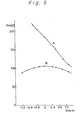
- the graph of Fig. 5 illustrates an example of measured values of R ON /R min as a function of amplitude (V DS ) corresponding to calculated values of Fig. '3.
- curve A relates to measured values for a previous circuit
- curve B relates to measured values for a circuit embodying the present invention.
- R ON in the embodiment of the present invention is much smaller than in the previous circuit.
- distortion resulting from variation in internal resistance of the switching circuit is reduced.
- second order distortion is reduced to a great extent.
- Fig. 6 is a circuit diagraph of an example of a switching circuit embodying the present invention.
- J 0 to J 2 designate field effect transistors which form a switching circuit as shown in Fig. 4.
- J 3 to J 6 are FETs.
- Q 1 to Q 5 and Q 6 are opposite type transistors (npn and pnp transistors) respectively, and R 1 to R 6 are resistors.
- Transistors J 5 , J6 and Q 6 work to generate the control voltage corresponding to E in Fig. 4.
- J 3 and J 4 has its gate and source electrodes shorted together, so each operates in a saturation region and works as a constant current source.
- J 3 works as a current source for E K and J 4 corresponds to the constant current source I D in Fig. 4.
- Resistors R 3 and R 4 divide the source or supply voltage V CC to supply base bias voltage to transistor Q 3 .
- R 5 and R 6 supply the base bias voltage of Q 4 by dividing V CC .
- the other transistors and resistors constitute a circuit to control E K .
- An analog signal applied between the terminals S and D of J 0 is gated (switched) on and off by a control signal applied to input terminal IN.
- the input control signal may be any type of on-off signal, such as the output signal of a logic circuit, for example.
- the emitter coupled transistor Q 2 When the switching signal applied to the terminal IN is low level, the emitter coupled transistor Q 2 is off, Q 3 is on, and current runs through the resistor R 1 .
- the circuit constants are selected to keep the voltage drop across the resistor R 1 higher than the pinch off voltage of J 5 .
- J 5 is cut off and current does not flow through J 6 .
- the gate and source of J 6 are shorted to one another and the voltage drop in the transistor J 6 is almost zero. In this case the gate control voltage of J 0 falls to the base-emitter voltage V BE of Q 6 (approximately 0.7 V), and the switching transistor J 0 becomes conductive, thus the analog signal applied the terminal S and D is passed (the gate is opened).
- Transistor Q 1 which is a npn transistor similar to Q 5 , has its base connected to its collector, and functions as a diode to provide same voltage drop of Q 1 (the same drop as Q 5 ) when J S is on (conductive). Thus, the gate-source voltage of J 5 is almost 0, and J 5 become conductive.
- Transistors J 5 and J6 are selected beforehand so that I DSS the saturation current of J 5 is much larger than (for example about 10 times as large as) that of J 6 .
- J S is operated in an unsaturated region
- J 6 is operated in a saturated region.
- the drain-source voltages V DS of J 5 and J 6 become respectively V DS5 ⁇ V p and V DS6 > V p . Therefore, the gate voltage of J O goes up alomost to the voltage of V CC , and it does not depend on the voltage of Q 6 .
- the gate transistor J 0 is pinched off, and analog signal applied between the terminals S and D is choked off (the gate is closed).
- Selection of saturation current of J 5 and J 6 is not critical; it is sufficient if, for example, the saturation current of J 6 is less than a quarter that of J 5 .
- Fig. 6 is an example of an embodiment of the present invention. Many other circuits may be devised in accordance with the present invention.
- a gate circuit embodying the present invention detects the voltage not only of the source but also of the drain side of a switching FET, and feeds back the detected voltages to correct the gate voltage.
- variation of on-state resistance of the FET is decreased and moreover, the on-state resistance varies symmetrically with respect to positive and negative voltages, so that second order distortion is reduced to a great extent.
- the invention has been described mainly in the context of a p-channel switching FET, but it will be clear that embodiments of the invention can be applied to n-channel switching FETs, merely by appropriate reversal of the polarity of applied voltages. They can also be applied to MOS type, junction type, and any other kind of field effect transistors.
Landscapes
- Electronic Switches (AREA)
- Junction Field-Effect Transistors (AREA)
Abstract
Description
- The present invention relates to a field effect transistor gate circuit for switching analog signals. More particularly, it is concerned with a gate circuit for switching analog signals on and off by means of field effect transistors.
- Switching of analog signals has generally been performed by relays, but recently it has become important to handle analog signals by means of semiconductor devices and this means that signal distortion has become an important factor. That is, a signal passed through a relay suffers no distortion, but a signal passed through semiconductor devices does.
- One approach used in an attempt to avoid distortion problems with analog signals handled by semiconductor devices is to handle only small signals. This approach has been tried because even if the semiconductor device transfer characteristic is not linear a small signal amplitude is not so distorted as a larger signal amplitude. However, the need to employ solid state switching devices is increasing, because of their small size, quick response, small operational power consumption, high reliabilitiy, economy and so on. Moreover, such devices are required which can handle larger amplitude signals.
- For switching signals, field effect transistors (FET) are widely used. However, in circuits which switch analog signals by turning FET's on and off, variation in the internal resistance of an FET when it is in an on state (on-resistance), according to the voltage between source and drain (source-drain voltage) and signal polarity causes distortion of signals passing through the FET.
- Fig. 1 is a schematic circuit diagram of a previous switching circuit for analog signals. In the Figure, J0 is a p-channel type FET for signal switching, ID is a constant current source supplying current to gate G of the FET J0 and so on. EK is a control voltage source varying the conductivity of FET JO and shifting the state of J0 on and off.
- The fundamental switching process in the circuit of Fig. 1 is performed by switching FET J0 on and off. Namely, when the control voltage provided by source EK is high, the channel between source S and the drain D of FET J0 is pinched off by a depletion layer which expands (extends) as a result of the high gate voltage applied to J0, and the switch is off (gate is closed). On the other hand, when the control voltage provided by source EK is low, the depletion layer contracts (narrows), and the switch is on (gate is opened). So, the state of the switch (the on-off state of the gate) is determined by the state, low or high, of the control voltage.
- FET J1 in Fig. 1 detects the voltage of the source S of FET J0 and provides feedback to the gate G of FET J0 in order to maintain the voltage between gate G and source S of J0 (VGS0) constant, independent to source voltage.
- FET drain current has saturation characteristics as shown in the graph of Fig. 2. The graph shows the drain current ID versus source-drain voltage VDS, for various values of voltage between gate and source (gate-source voltage) VGS. As can be seen from the graph drain current has a saturation region and on unsaturation region.
- In the saturation region, the drain current ID can be expressed as

- In the unsaturation region, the drain current ID is given by.

- These equations are well known. More detail is given in, for example, Physics of Semi-conductor Devices: John Wiley & Sons, Inc. N.Y. 1969.
- In the circuit of Fig. 1, the drain current of FET J1 is determined by ID, a constant current source. Because in this case EK is in high level, so the gates of J0 and J1 are highly biased against each source electrode, and therefore the gate currents of J0 and J1 do not flow. Thus, according to equation (1), VGS1 the gate-source voltage of J1 becomes constant. In the same manner, VGSO the gate-source voltage of FET J0 also becomes constant independent of VDS.
- RON' the resistance between source and drain of transistor J0 when it is in an ON (conductive) state, is given by

- It should be notd that equation (2) is expressed in terms of absolute values, whilst for a general p-channel FET, VGS is positively and VDS is negatively biased. It is necessary, therefore, to replace VDS in the above equation by -VDSO. Therefore

- When VDS>0, the drain current ID of a p-channel FET is controlled by VGD, the gate-drain voltage (contrary to the above-mentioned case, in which VGS is controlling) and

- From this and from equation (4), RON is given by

- This is the same equation as (3) except that there is no restricton on the sign of V DS.
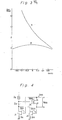
- In the graph of Fig. 3, curve A illustrates the relationship of equation (5) [and equation (3)], under conditions that |VP|>|VGS|, and |Vp|> |VGD|. As can be seen in the graph, in the region where V <0, RON increases, whilst in the region where VDS>0, RON decreases as compared to its value at VDS = 0, giving an asymmetric characteristic for RON as seen in the graph of Fig. 3.
- For the graph of Fig. 3 values were calculated from equation (5) with Vp= 1.5 volt, VGSO = 0.8 volt (at) and VDS0 = 0.
- The asymmetric RON characteristic seen in the graph gives rise to asymmetric current and voltage characteristics for signals passing through the FET, which causes distortion as mentioned above.
- According to the present invention, there is provided a gate circuit, employing field effect transistors for switching analog signals, comprising:
- a first field effect transistor (FET), for switching on and off an input signal supplied to the gate circuit;
- a control voltage source operable to control the gate voltage of the first FET and to control the conductance of the first FET;
- a second FET arranged for detecting the source voltage of the first FET and operable to keep variation of the voltage between the gate and the source of the first FET small when the first FET is in a conductive state;
- a third FET arranged for detecting the drain voltage of the first FET and operable to keep variation of the voltage between the gate and drain of the first FET small when the first FET is in a conductive state; and
- a constant current source arranged for supplying a constant current to the second and third FETs.
- An embodiment of the present invention can provide a gate circuit (a switching circuit) from field effect transistors, in which distortion is reduced.
- In a gate circuit embodying the present invention the distortion of signals passing through the circuit is reduced by effecting an improvement in relation to the unsymmetrical characteristics of internal resistance when the circuit is in an on state.
- An embodiment of the present invention can provide a gate circuit (a switchng circuit) of field effect transistors whose ON state source-drain internal resistance (RON) is small and is symmetrical with respect to source-drain voltage (VDS), thus reducing second order distortion.
- Briefly, in an embodiment of the present invention, source side and drain side voltages of a switching transistor are detected and appropriately fed back to the gate of the transistor. By such feedback the resistance of the switching transistor becomes small and symmetric with respect to the zero point of source-drain voltage.
- Reference is made, by way of example, to the accompanying drawings, in which:-
- Fig. 1 is a schematic circuit diagram of main parts of a previous switching circuit using of field effect transistors;
- Fig. 2 is a graph illustrating static characterisitics of a field effect transistor,
- Fig. 3 is a graph illustrating calculated on-state resistance characteristics of the previous switching circuit (curve A) and a circuit embodying the present invention (curve B),
- Fig. 4 is a schematic circuit diagram of main parts of a switching circuit embodying the present invention,
- Fig. 5 is a graph illustrating measured on-state resistance characteristics of a previous switching circuit (curve A) and a circuit embodying the present invention (curve B), and
- Fig. 6 is a circuit diagram of an embodiment of the present invention.
- The switching circuit of Fig. 4, embodying the present invention, is provided with an additional field effect transistor (FET) J2 as compared with Fig. 1. Transistor J2 detects the drain voltage of FET J0 and corrects the gate voltage of JO. In this circuit, the field effect transistor J should have a symmetrical source-drain current vs source-drain voltage characteristic, when the polarity of the voltage is reversed (that is, when the source and drain electrodes are connected one in place of the other). But it is well known that conventional FETs usually have such symmetrical characteristics.
- In the circuit of Fig. 4, when the absolute value of YDS0, the source-drain voltage of J0, is high, the gate voltage of field effect transistor J0 is controlled by that one of FETs J1 or J2 whose gate is connected to the lower voltage side of J0, because the drain and source electrodes of J1 and J2 are commonly connected to the voltage voltage source EK and to ground respectively. Thus, the transistor (J1 or J2) whose gate is connected to the higher voltage side will be pinched off, and the transistor (J2 or J1) whose gate is connected to the lower voltage side controls the gate of J0.
- In a case in which VDSO is not so high, the situation is almost the same, and J0 is mainly controlled by that one of J1 or J2 whose gate voltage is connected to the lower voltage.
- Namely, when VDS0<0 (which means that the voltage of drain D of J0 is lower than that of source S of J0), the FET J0 is controlled by J2. In this case, J1 can be neglected because it is pinched off. J2 is conductive and the current running through J2 is constant current I D. So, V GS2 is constant, independent to its gate voltage. Thus, the gate voltage of J0 (VGSO) becomes lower than at VDSO = 0, because drain voltage is lower than source voltage. Further RON, the resistance between source and drain of J0, decreases below its value at VDS=0. This will be understood from the graph of Fig. 2, showing FET characteristics. As VGS decreases, the applicable VDS versus ID curve shifts towards that applicable for VGS = 0, and the gradient of the applicable curve in the unsaturation region becomes steeper. Thus, the differential conductance increases, and R0 (the inverse of conductance) decreases.
- On the other hand when VDS0> 0 (that is, the voltage of drain D of JO is higher than the voltage of its source S) the FET J1 controls J0. In this case, by reason of the aforementioned symmetrical characteristics of FET J0, the situation is same except that the source and drain of J0 are effectively interchanged. Thus, the resistance R0 again decreases, as shown by curve B in the graph of Fig. 3.
- The above-explained performance of the circuit of Fig. 4 can be analysed with the assistance of some equations. For the sake of simplicity, it is assumed that R min' IDSS and Vp of J1 are equal to those of J2. Since the circuit is operated by a constant current source, and ID is the sum of the drains current IDI and ID2 of J1 and J2, it is obtained from equation (1) that


- It should be noted that equation (2) is expressed in terms of absolute values. For a general p-channel FET, VGS is positively and VDS is negatively biased and it is necessary, therefore, to replace VDSO in the above equation by -VDS0. Therefore

- Substituting (7) into (6) and eliminating VGS2' the following is obtained

- In this equation, the - sign of ± should be chosen. The reason for this is that for VDS0= 0, VGS should be larger than Vp. Therefore


- In the graph of Fig. 3, the RON characteristic corresponding to a circuit of Fig. 4 is shown by curve B. For deriving the curve B it was taken that Vp = 1.5 volt, VGS0 = 0.8 volt (VDSO = 0), ID/IDSS= 0.5 (namely, VGS1=VGS2=0·44 volts V DSO = 0), EK= 1.24 volt. As can be see in the graph RON decreases on both sides of VDS=0 regardless of source-drain voltage polarity.
- The graph of Fig. 5 illustrates an example of measured values of RON/Rmin as a function of amplitude (VDS) corresponding to calculated values of Fig. '3. In the graph of Fig. 5 curve A relates to measured values for a previous circuit, and curve B relates to measured values for a circuit embodying the present invention. As can be seen, the embodiment of present invention offers a significant improvement. Further it will be seen that there is good agreement between measured and calculated characteristics. RON in the embodiment of the present invention is much smaller than in the previous circuit. Moreover, curve B has a gentle slope as compared to curve A, and it is symmetric on both sides of VDS = 0. Thus, distortion resulting from variation in internal resistance of the switching circuit is reduced. In particular second order distortion is reduced to a great extent.
- The description given above in relation to the present invention has been concerned with a circuit using p-channel type FETs. However it will be clear to those skilled in the art that the invention can also be applied to circuits using n-channel type FETs by appropriately reversing the polarities of voltages applied to parts of the circuit. It will be also clear that any kind of field effect transistor, such as MOS (metal oxide semiconductor) type or junction type FETs, can be applied in embodiments of the present invention. For the sake of simplicity, the description hereinafter will also be given with respect to p-channel FETs.
- Fig. 6 is a circuit diagraph of an example of a switching circuit embodying the present invention. In Figure 6, J0 to J2 designate field effect transistors which form a switching circuit as shown in Fig. 4. J3 to J6 are FETs. Q1 to Q5 and Q6 are opposite type transistors (npn and pnp transistors) respectively, and R1 to R6 are resistors.
- Transistors J5, J6 and Q6 work to generate the control voltage corresponding to E in Fig. 4.
- Each of J3 and J4 has its gate and source electrodes shorted together, so each operates in a saturation region and works as a constant current source. J3 works as a current source for EK and J4 corresponds to the constant current source ID in Fig. 4.
- Resistors R3 and R4 divide the source or supply voltage VCC to supply base bias voltage to transistor Q3. Similarly, R5 and R6 supply the base bias voltage of Q4 by dividing VCC. The other transistors and resistors constitute a circuit to control EK.
- An analog signal applied between the terminals S and D of J0 is gated (switched) on and off by a control signal applied to input terminal IN. The input control signal may be any type of on-off signal, such as the output signal of a logic circuit, for example.
- Operation of the cirucit of Fig. 6 is as follows.
- When the switching signal applied to the terminal IN is low level, the emitter coupled transistor Q2 is off, Q3 is on, and current runs through the resistor R1. The circuit constants are selected to keep the voltage drop across the resistor R1 higher than the pinch off voltage of J5. Thus, J5 is cut off and current does not flow through J6. Moreover, the gate and source of J6 are shorted to one another and the voltage drop in the transistor J6 is almost zero. In this case the gate control voltage of J0 falls to the base-emitter voltage V BE of Q6 (approximately 0.7 V), and the switching transistor J0 becomes conductive, thus the analog signal applied the terminal S and D is passed (the gate is opened).
- When the control signal applied to the terminal IN is high level, on the other hand, transistor Q2 is on, Q3 is off and the voltage drop across resistor R1 becomes negligible. The transistors Q 5 and J5 become conductive. Transistor Q1, which is a npn transistor similar to Q5, has its base connected to its collector, and functions as a diode to provide same voltage drop of Q1 (the same drop as Q5) when JS is on (conductive). Thus, the gate-source voltage of J5 is almost 0, and J5 become conductive. Transistors J5 and J6 are selected beforehand so that I DSS the saturation current of J5 is much larger than (for example about 10 times as large as) that of J6. Therefore, in this case, JS is operated in an unsaturated region, and J6 is operated in a saturated region. The drain-source voltages VDS of J5 and J6 become respectively VDS5 <Vp and VDS6> Vp. Therefore, the gate voltage of JO goes up alomost to the voltage of VCC, and it does not depend on the voltage of Q6. Thus, the gate transistor J0 is pinched off, and analog signal applied between the terminals S and D is choked off (the gate is closed). Selection of saturation curent of J5 and J6 is not critical; it is sufficient if, for example, the saturation current of J6 is less than a quarter that of J5.
- In the above manner the switching circuit for analog signals is operated. The circuit shown in Fig. 6 is an example of an embodiment of the present invention. Many other circuits may be devised in accordance with the present invention.
- It will be seen, by comparing the circuit of Fig. 6 with the circuit of Fig. 4, that in Fig. 6 the drain electrodes of J1 and J2 are connectedto a negative voltage -VEE. Thereby, the circuit of Fig. 6 is operable for both positive and negative signed analog signals. The ground (earth) voltage is used as a reference voltage of a logic circuit.
- As described above, a gate circuit embodying the present invention detects the voltage not only of the source but also of the drain side of a switching FET, and feeds back the detected voltages to correct the gate voltage. Thus, variation of on-state resistance of the FET is decreased and moreover, the on-state resistance varies symmetrically with respect to positive and negative voltages, so that second order distortion is reduced to a great extent.
- As has been stated above, the invention has been described mainly in the context of a p-channel switching FET, but it will be clear that embodiments of the invention can be applied to n-channel switching FETs, merely by appropriate reversal of the polarity of applied voltages. They can also be applied to MOS type, junction type, and any other kind of field effect transistors.
Claims (6)
Applications Claiming Priority (2)
| Application Number | Priority Date | Filing Date | Title |
|---|---|---|---|
| JP192952/82 | 1982-11-02 | ||
| JP57192952A JPS5981920A (en) | 1982-11-02 | 1982-11-02 | Analog switch circuit |
Publications (3)
| Publication Number | Publication Date |
|---|---|
| EP0108603A2 true EP0108603A2 (en) | 1984-05-16 |
| EP0108603A3 EP0108603A3 (en) | 1986-02-05 |
| EP0108603B1 EP0108603B1 (en) | 1988-06-29 |
Family
ID=16299745
Family Applications (1)
| Application Number | Title | Priority Date | Filing Date |
|---|---|---|---|
| EP83306657A Expired EP0108603B1 (en) | 1982-11-02 | 1983-11-02 | Field effect transistor gate circuit for switching analog signals |
Country Status (4)
| Country | Link |
|---|---|
| US (1) | US4551644A (en) |
| EP (1) | EP0108603B1 (en) |
| JP (1) | JPS5981920A (en) |
| DE (1) | DE3377258D1 (en) |
Cited By (1)
| Publication number | Priority date | Publication date | Assignee | Title |
|---|---|---|---|---|
| US4765184A (en) * | 1986-02-25 | 1988-08-23 | Delatorre Leroy C | High temperature switch |
Family Cites Families (15)
| Publication number | Priority date | Publication date | Assignee | Title |
|---|---|---|---|---|
| US3313358A (en) * | 1964-04-01 | 1967-04-11 | Chevron Res | Conductor casing for offshore drilling and well completion |
| CA810796A (en) * | 1966-07-25 | 1969-04-15 | International Business Machines Corporation | Field-effect, electronic switch |
| US3558921A (en) * | 1967-01-23 | 1971-01-26 | Hitachi Ltd | Analog signal control switch |
| US3519852A (en) * | 1967-09-26 | 1970-07-07 | Westinghouse Electric Corp | Low power analog switch |
| US3740581A (en) * | 1972-03-08 | 1973-06-19 | Hughes Aircraft Co | Precision switching circuit for analog signals |
| JPS501630A (en) * | 1973-05-04 | 1975-01-09 | ||
| JPS5010545A (en) * | 1973-05-24 | 1975-02-03 | ||
| US3902078A (en) * | 1974-04-01 | 1975-08-26 | Crystal Ind Inc | Analog switch |
| US3916222A (en) * | 1974-05-28 | 1975-10-28 | Nat Semiconductor Corp | Field effect transistor switching circuit |
| US3955103A (en) * | 1975-02-12 | 1976-05-04 | National Semiconductor Corporation | Analog switch |
| US4042836A (en) * | 1976-04-12 | 1977-08-16 | National Semiconductor Corporation | Field effect transistor switch |
| US4103186A (en) * | 1977-03-24 | 1978-07-25 | National Semiconductor Corporation | Low power jfet switch |
| JPS5647128A (en) * | 1979-09-26 | 1981-04-28 | Matsushita Electric Ind Co Ltd | Switch circuit |
| JPS6049378B2 (en) * | 1980-03-29 | 1985-11-01 | 日本ビクター株式会社 | FET switch circuit |
| DE3226339C2 (en) * | 1981-07-17 | 1985-12-19 | Tokyo Shibaura Denki K.K., Kawasaki, Kanagawa | Analog switch device with MOS transistors |
-
1982
- 1982-11-02 JP JP57192952A patent/JPS5981920A/en active Granted
-
1983
- 1983-10-31 US US06/547,236 patent/US4551644A/en not_active Expired - Fee Related
- 1983-11-02 EP EP83306657A patent/EP0108603B1/en not_active Expired
- 1983-11-02 DE DE8383306657T patent/DE3377258D1/en not_active Expired
Cited By (1)
| Publication number | Priority date | Publication date | Assignee | Title |
|---|---|---|---|---|
| US4765184A (en) * | 1986-02-25 | 1988-08-23 | Delatorre Leroy C | High temperature switch |
Also Published As
| Publication number | Publication date |
|---|---|
| DE3377258D1 (en) | 1988-08-04 |
| EP0108603B1 (en) | 1988-06-29 |
| JPH035690B2 (en) | 1991-01-28 |
| US4551644A (en) | 1985-11-05 |
| JPS5981920A (en) | 1984-05-11 |
| EP0108603A3 (en) | 1986-02-05 |
Similar Documents
| Publication | Publication Date | Title |
|---|---|---|
| US4492883A (en) | Unpowered fast gate turn-off FET | |
| US4958089A (en) | High output drive FET buffer for providing high initial current to a subsequent stage | |
| US5347169A (en) | Inductive load dump circuit | |
| US4477742A (en) | Three terminal bidirectional drain to drain FET circuit | |
| US4952827A (en) | Circuit arrangement for controlling the load current in a power MOSFET | |
| US5767721A (en) | Switch circuit for FET devices having negative threshold voltages which utilize a positive voltage only | |
| US4001606A (en) | Electrical circuit | |
| US6046622A (en) | Electronic analogue switch | |
| US12525977B2 (en) | Gate drive apparatus and control method | |
| EP3522374A1 (en) | A switch circuit, corresponding device and method | |
| US4256974A (en) | Metal oxide semiconductor (MOS) input circuit with hysteresis | |
| US4321491A (en) | Level shift circuit | |
| US4798979A (en) | Schottky diode logic for E-mode FET/D-mode FET VLSI circuits | |
| JPH07142990A (en) | Level conversion circuit | |
| JPH06177733A (en) | Drive circuit of power mosfet | |
| US4558237A (en) | Logic families interface circuit and having a CMOS latch for controlling hysteresis | |
| US6031392A (en) | TTL input stage for negative supply systems | |
| US6900711B2 (en) | Switching system | |
| US5420527A (en) | Temperature and supply insensitive TTL or CMOS to 0/-5 V translator | |
| EP0108603B1 (en) | Field effect transistor gate circuit for switching analog signals | |
| US20210211128A1 (en) | Gate Drive Apparatus and Control Method | |
| US5055723A (en) | Jfet analog switch with gate current control | |
| US4837458A (en) | Flip-flop circuit | |
| EP2264900B1 (en) | Low-current inverter circuit | |
| US5546040A (en) | Power efficient transistor and method therefor |
Legal Events
| Date | Code | Title | Description |
|---|---|---|---|
| PUAI | Public reference made under article 153(3) epc to a published international application that has entered the european phase |
Free format text: ORIGINAL CODE: 0009012 |
|
| AK | Designated contracting states |
Designated state(s): DE FR GB |
|
| PUAL | Search report despatched |
Free format text: ORIGINAL CODE: 0009013 |
|
| AK | Designated contracting states |
Designated state(s): DE FR GB |
|
| 17P | Request for examination filed |
Effective date: 19860206 |
|
| 17Q | First examination report despatched |
Effective date: 19870327 |
|
| GRAA | (expected) grant |
Free format text: ORIGINAL CODE: 0009210 |
|
| AK | Designated contracting states |
Kind code of ref document: B1 Designated state(s): DE FR GB |
|
| REF | Corresponds to: |
Ref document number: 3377258 Country of ref document: DE Date of ref document: 19880804 |
|
| ET | Fr: translation filed | ||
| PLBE | No opposition filed within time limit |
Free format text: ORIGINAL CODE: 0009261 |
|
| STAA | Information on the status of an ep patent application or granted ep patent |
Free format text: STATUS: NO OPPOSITION FILED WITHIN TIME LIMIT |
|
| 26N | No opposition filed | ||
| PGFP | Annual fee paid to national office [announced via postgrant information from national office to epo] |
Ref country code: GB Payment date: 19920903 Year of fee payment: 10 |
|
| PGFP | Annual fee paid to national office [announced via postgrant information from national office to epo] |
Ref country code: FR Payment date: 19921127 Year of fee payment: 10 |
|
| PGFP | Annual fee paid to national office [announced via postgrant information from national office to epo] |
Ref country code: DE Payment date: 19930129 Year of fee payment: 10 |
|
| PG25 | Lapsed in a contracting state [announced via postgrant information from national office to epo] |
Ref country code: GB Effective date: 19931102 |
|
| GBPC | Gb: european patent ceased through non-payment of renewal fee |
Effective date: 19931102 |
|
| PG25 | Lapsed in a contracting state [announced via postgrant information from national office to epo] |
Ref country code: FR Effective date: 19940729 |
|
| PG25 | Lapsed in a contracting state [announced via postgrant information from national office to epo] |
Ref country code: DE Effective date: 19940802 |
|
| REG | Reference to a national code |
Ref country code: FR Ref legal event code: ST |