EP0109084A1 - Doppelseitig gedruckte Dickfilm-Leiterplatte und Verfahren zu ihrer Herstellung - Google Patents
Doppelseitig gedruckte Dickfilm-Leiterplatte und Verfahren zu ihrer Herstellung Download PDFInfo
- Publication number
- EP0109084A1 EP0109084A1 EP19830111383 EP83111383A EP0109084A1 EP 0109084 A1 EP0109084 A1 EP 0109084A1 EP 19830111383 EP19830111383 EP 19830111383 EP 83111383 A EP83111383 A EP 83111383A EP 0109084 A1 EP0109084 A1 EP 0109084A1
- Authority
- EP
- European Patent Office
- Prior art keywords
- bore
- substrate
- hole
- thick
- gorge
- Prior art date
- Legal status (The legal status is an assumption and is not a legal conclusion. Google has not performed a legal analysis and makes no representation as to the accuracy of the status listed.)
- Granted
Links
- 238000004519 manufacturing process Methods 0.000 title claims abstract description 8
- 239000000758 substrate Substances 0.000 claims abstract description 94
- 239000000126 substance Substances 0.000 claims abstract description 51
- 238000000034 method Methods 0.000 claims abstract description 22
- 238000010304 firing Methods 0.000 claims abstract description 7
- 239000007788 liquid Substances 0.000 claims abstract description 6
- 239000000463 material Substances 0.000 claims abstract description 3
- 238000001035 drying Methods 0.000 claims description 8
- 238000005553 drilling Methods 0.000 claims description 2
- 239000000919 ceramic Substances 0.000 claims 1
- 238000007639 printing Methods 0.000 abstract description 13
- 238000007650 screen-printing Methods 0.000 abstract description 11
- 229910010293 ceramic material Inorganic materials 0.000 abstract description 8
- 230000004323 axial length Effects 0.000 description 5
- 239000004020 conductor Substances 0.000 description 3
- KDLHZDBZIXYQEI-UHFFFAOYSA-N Palladium Chemical compound [Pd] KDLHZDBZIXYQEI-UHFFFAOYSA-N 0.000 description 2
- 229910003460 diamond Inorganic materials 0.000 description 2
- 239000010432 diamond Substances 0.000 description 2
- 230000004048 modification Effects 0.000 description 2
- 238000012986 modification Methods 0.000 description 2
- 239000011324 bead Substances 0.000 description 1
- 230000003247 decreasing effect Effects 0.000 description 1
- 239000012776 electronic material Substances 0.000 description 1
- TWNQGVIAIRXVLR-UHFFFAOYSA-N oxo(oxoalumanyloxy)alumane Chemical compound O=[Al]O[Al]=O TWNQGVIAIRXVLR-UHFFFAOYSA-N 0.000 description 1
- 229910052763 palladium Inorganic materials 0.000 description 1
- 238000004080 punching Methods 0.000 description 1
- 229910052709 silver Inorganic materials 0.000 description 1
- 239000004332 silver Substances 0.000 description 1
Images
Classifications
-
- H—ELECTRICITY
- H05—ELECTRIC TECHNIQUES NOT OTHERWISE PROVIDED FOR
- H05K—PRINTED CIRCUITS; CASINGS OR CONSTRUCTIONAL DETAILS OF ELECTRIC APPARATUS; MANUFACTURE OF ASSEMBLAGES OF ELECTRICAL COMPONENTS
- H05K3/00—Apparatus or processes for manufacturing printed circuits
- H05K3/40—Forming printed elements for providing electric connections to or between printed circuits
- H05K3/4038—Through-connections; Vertical interconnect access [VIA] connections
- H05K3/4053—Through-connections; Vertical interconnect access [VIA] connections by thick-film techniques
- H05K3/4061—Through-connections; Vertical interconnect access [VIA] connections by thick-film techniques for via connections in inorganic insulating substrates
-
- H—ELECTRICITY
- H05—ELECTRIC TECHNIQUES NOT OTHERWISE PROVIDED FOR
- H05K—PRINTED CIRCUITS; CASINGS OR CONSTRUCTIONAL DETAILS OF ELECTRIC APPARATUS; MANUFACTURE OF ASSEMBLAGES OF ELECTRICAL COMPONENTS
- H05K1/00—Printed circuits
- H05K1/02—Details
- H05K1/03—Use of materials for the substrate
- H05K1/0306—Inorganic insulating substrates, e.g. ceramic, glass
-
- H—ELECTRICITY
- H05—ELECTRIC TECHNIQUES NOT OTHERWISE PROVIDED FOR
- H05K—PRINTED CIRCUITS; CASINGS OR CONSTRUCTIONAL DETAILS OF ELECTRIC APPARATUS; MANUFACTURE OF ASSEMBLAGES OF ELECTRICAL COMPONENTS
- H05K2201/00—Indexing scheme relating to printed circuits covered by H05K1/00
- H05K2201/09—Shape and layout
- H05K2201/09818—Shape or layout details not covered by a single group of H05K2201/09009 - H05K2201/09809
- H05K2201/09827—Tapered, e.g. tapered hole, via or groove
-
- H—ELECTRICITY
- H05—ELECTRIC TECHNIQUES NOT OTHERWISE PROVIDED FOR
- H05K—PRINTED CIRCUITS; CASINGS OR CONSTRUCTIONAL DETAILS OF ELECTRIC APPARATUS; MANUFACTURE OF ASSEMBLAGES OF ELECTRICAL COMPONENTS
- H05K2201/00—Indexing scheme relating to printed circuits covered by H05K1/00
- H05K2201/09—Shape and layout
- H05K2201/09818—Shape or layout details not covered by a single group of H05K2201/09009 - H05K2201/09809
- H05K2201/09981—Metallised walls
-
- H—ELECTRICITY
- H05—ELECTRIC TECHNIQUES NOT OTHERWISE PROVIDED FOR
- H05K—PRINTED CIRCUITS; CASINGS OR CONSTRUCTIONAL DETAILS OF ELECTRIC APPARATUS; MANUFACTURE OF ASSEMBLAGES OF ELECTRICAL COMPONENTS
- H05K3/00—Apparatus or processes for manufacturing printed circuits
- H05K3/10—Apparatus or processes for manufacturing printed circuits in which conductive material is applied to the insulating support in such a manner as to form the desired conductive pattern
- H05K3/12—Apparatus or processes for manufacturing printed circuits in which conductive material is applied to the insulating support in such a manner as to form the desired conductive pattern using thick film techniques, e.g. printing techniques to apply the conductive material or similar techniques for applying conductive paste or ink patterns
- H05K3/1216—Apparatus or processes for manufacturing printed circuits in which conductive material is applied to the insulating support in such a manner as to form the desired conductive pattern using thick film techniques, e.g. printing techniques to apply the conductive material or similar techniques for applying conductive paste or ink patterns by screen printing or stencil printing
Definitions
- the present invention relates to a method of making a double-sided thick-film integrated circuit.
- Such integrated circuits may be made by applying a conductive viscous liquid substance or ink to opposite sides of a plate-shaped thick-film substrate of a ceramic material in patterns defining the circuits desired.
- the conductive substance is normally applied by alternating screen printing and drying processes.
- the substrate In order to secure that an amount of the conductive substance sufficient to establish contact between the opposite sides of the substrate, is introduced into the very thin bores during a printing operation, the substrate is placed on a suction box so as to establish a pressure difference between the opposite sides of the substrate. In this manner it may be secured that the bore is filled with the conductive substance in a controlled manner.
- the conductive substance In order to secure contact with a circuit which is subsequently printed on the side of the substrate facing the suction box, the conductive substance must be sucked right through the bore so that the risk of smearing the substance renders it impossible to transport the substrate by means of conveyor belts, until the conductive substance has been dried, and, consequently, the use of special handling equipment is necessary.
- the present invention provides a method making it possible to produce double-sided thick-film integrated circuits by using conventional printers and unloaders.
- the present invention provides a method of making a double-sided thick-film integrated circuit, said method comprising
- a gorge or throat - which means a restriction extending along a relatively small axial length of the bore - having a suitably small diameter or cross-sectional area, which may be of substantially the same order as the diameter or cross-sectional area of the conventional straight bores. Furthermore, the small axial extension of the gorge or throat makes it possible to completely fill the hole or bore by the screen printing operations on both sides of the substrate without the necessity of providing a pressure difference between the opposite side surfaces of the substrate.
- the gorge or throat may be located at any position along the axial length of the through bore or hole, and as only a very small amount of conductive substance penetrates the gorge or throat during a screen printing operation of one side of the substrate, the risk of smearing the substance on the opposite side of the substrate during handling thereof may be avoided.
- the gorge or throat of the through bore may be located between two widened end portions of the bore. In this case it is less important which one of the opposite side surfaces of the substrate is printed at first.
- the widenings at the opposite ends of the bore may have any cross-sectional shape, for example a cylindrical, conical, or spherical shape. I n the preferred embodiment, however, the cross-sectional area of the widened end portions is decreasing from the outer side surfaces of the substrate towards the gorge or throat so that the bore or hole is substantially hourglass-shaped.
- the gorge or throat is located closely adjacent to the said first side surface of the substrate, which is the side surface to which conductive substance is applied at first.
- the widened end portion of the bore is automatically filled up with conductive substance so as to establish contact between the printed circuits on the opposite sides of the substrate.
- the hole or bore may be funnel-shaped and may, for example be in the form of a truncated cone.
- the widened end portion may have any other shape, such as cylindrical or spherical.
- the hole or bore in the substrate may be made in any suitable manner.
- the hole or bore is made by making a straight bore with a diameter corresponding to that of the gorge or throat, for example by means of a laser beam, and subsequently widening the end portion or portions of the straight bore by means of a grinding tool. It is envisaged, however, that it is also possible to make the hole or bore in its final shape by a laser drilling or laser shooting technique.
- the diameter or cross-sectional area of the gorge or throat must be adapted to the viscosity of the conductive substance or ink so that during screen printing of the first side surface of the substrate a very small amount of the substance is squeezed through the gorge or throat without being able to flow freely therethrough.
- the substrate is made from a wet ceramic material which is formed into small plates or sheets in its wet condition and thereafter hardened by firing.
- the through holes or bores are provided in the substrate after firing and before printing.
- the bore or hole may be formed, for example by punching, while the substrate is in a rather soft condition, for example after drying the wet ceramic material, but prior to firing.
- the present invention also relates to a double-sided thick-film integrated circuit comprising
- the present invention provides a thick-film substrate defining therein a transversely extending through hole or bore having at least one widened end portion merging into a gorge or throat.
- the present invention also provides a method of making such a thick-film substrate by forming the substrate from a wet deformable ceramic material, drying the wet substrate, forming the hole or bore in the dried substrate, and subsequently firing the substrate thus formed to harden it.
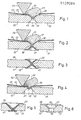
- Figs. 1 - 3 illustrate a method of making a double-sided thick-film integrated circuit.
- Fig. 1 shows a pattern of a viscous conductive substance or ink 10 being applied to a first side surface 11 of a plate-shaped conventional thick-film substrate 12 by a conventional screen printing technique.
- the screen printing is made by means of a screen 13 having cut-outs or openings 18 therein corresponding to the said pattern, and by means of-a squeegee 14.
- the substrate 12 has one or more through holes or bores 15 formed therein, and each hole 15 (only one hole is shown in the drawings) is formed with a gorge or throat 16. In the embodiment shown in Figs.
- the hole 15 is hourglass-shaped and has widened end portions 17 on either side of the throat 16.
- the size of the widened end portions 17 is such that the widened end portion adjacent to the screen 13 will be filled with the viscous or paste-like substance 10 when this substance is pushed along the outer surface of the screen 13 and over the opening 18 therein by the squeegee 14 during the printing operation.
- the cross-sectional area and the axial length of the gorge or throat 16 is adapted to the viscosity of the substance 10 so that during the printing operation the substance is squeezed into the throat 16, but will not flow through the same, vide Fig. 1.
- the substrate When the print of conductive substance made on the first side surface 11 of the substrate 12 has been dried, the substrate is turned, and a desired circuit or pattern is printed on the opposite second side surface 19 of the substrate 12 by a similar conventional printing process using a screen 13 having openings or cutouts 18 therein corresponding to the desired pattern or print, vide Fig. 2.
- a desired circuit or pattern is printed on the opposite sides of the substrate 12 by a similar conventional printing process using a screen 13 having openings or cutouts 18 therein corresponding to the desired pattern or print, vide Fig. 2.
- patterns printed on the opposite sides of the substrate 12 are different.
- the two patterns or circuits comprise oppositely arranged points on the axis of the bore 15 which points are intended to be interconnected by a conductive interconnection 20.
- the adjacent widened end portion 17 is filled with the conductive substance 10 which is also squeezed into the gorge or throat 16 and united with substance 10 introduced into the gorge or throat from the other side of the substrate, so as to form the desired interconnection 20 of the circuits printed on opposite sides of the substrate 12.
- the ink or substance 10 will shrink so that the final shape of the dried substance in the bore or hole 15 will be as illustrated in Fig. 3.
- Figs. 4 and 5 show a substrate 12 with a substantially cone- or funnel-shaped bore or hole 15 comprising a gorge or throat 16 positioned closely adjacent to the first side surface 11, and a widened or funnel-shaped portion 21 located adjacent to the second side surface 19 of the substrate 12.
- the ink or substance 10 is squeezed through the adjacent throat 16 so as to form a bead at the inner part of the widened or funnel-shaped portion 21.
- the widened portion 21 of the bore 15 is filled with ink or substance 10 so as to provide a conductive interconnection 22 between the circuits on the opposite sides of the substrate 12. After drying the substance introduced into the bore 15 will have obtained a shape substantially as shown in Fig. 5.
- Fig. 6 shows a fragmentary sectional view of a thick-film substrate 12 with a modified funnel-shaped bore or hole 15.
- the gorge or throat 16 at the first side surface 11 of the substrate is part of a cylindrical bore having a widened end portion 17 at the opposite second side surface 19 of the substrate 12.
- the dry conductive substance may have a shape as indicated with broken lines in Fig. 6.
- the through holes 15 may be made in two stages. Firstly, a straight cylindrical bore with a diameter corresponding to that of the gorge or throat 16 may be made by laser beams, and, subsequently, the widened end portion or portions 17 and 21 may be made by grinding, for example by means of a diamond tool. Alternatively, it is possible to form the through openings 15 in the substrate 12 by suitable tools while the substrate is still in a soft or plastic condition, prior to firing the ceramic material.
- a standard type thick-film substrate of a ceramic material containing 96% of aluminum oxide was provided with through openings of the type shown in Figs. 1 - 3.
- the thickness of the substrate was 0.63 mm, and through bores with a diameter of 0.4 mm were made in the substrate by laser beam shooting.
- Each bore was provided with widened end portions by means of a spherical diamond grinding tool so as to provide widened end portions with spherical surfaces.
- the axial length of the gorge or throat defined between the widened end portions was approximately 0.1 mm, and the diameter of the widened end portions at the opposite side surfaces of the substrate was approximately 1 mm.
- Patterns of a palladium/silver conductor composition marketed by Dupont EMD Electronic Materials Division under No.
- Example 2 The procedure described in Example 1 was repeated with the modification that a widened, conical end portion was provided only at one end of each through bore so as to provide openings of the type shown in Fig. 6.
- the axial length of the gorge or throat was 0.3 mm, and the maximum diameter of the widened conical end portion at the outer side surface of the substrate was about 1.2 mm.
- the substrate was printed with a conductive substance as described in Example 1, and the same good result was obtained.
- the widened end portions 17 and 21 need not have a tapered section as shown, and may, for example, have a rectangular axial section.
Landscapes
- Engineering & Computer Science (AREA)
- Chemical & Material Sciences (AREA)
- Inorganic Chemistry (AREA)
- Manufacturing & Machinery (AREA)
- Microelectronics & Electronic Packaging (AREA)
- Printing Elements For Providing Electric Connections Between Printed Circuits (AREA)
Applications Claiming Priority (2)
| Application Number | Priority Date | Filing Date | Title |
|---|---|---|---|
| DK5087/82 | 1982-11-15 | ||
| DK508782 | 1982-11-15 |
Publications (2)
| Publication Number | Publication Date |
|---|---|
| EP0109084A1 true EP0109084A1 (de) | 1984-05-23 |
| EP0109084B1 EP0109084B1 (de) | 1987-06-10 |
Family
ID=8139329
Family Applications (1)
| Application Number | Title | Priority Date | Filing Date |
|---|---|---|---|
| EP19830111383 Expired EP0109084B1 (de) | 1982-11-15 | 1983-11-14 | Doppelseitig gedruckte Dickfilm-Leiterplatte und Verfahren zu ihrer Herstellung |
Country Status (2)
| Country | Link |
|---|---|
| EP (1) | EP0109084B1 (de) |
| DE (1) | DE3372054D1 (de) |
Cited By (8)
| Publication number | Priority date | Publication date | Assignee | Title |
|---|---|---|---|---|
| EP0138671A3 (de) * | 1983-09-21 | 1986-08-06 | Allied Corporation | Verfahren zur Herstellung einer gedruckten Schaltung |
| GB2188194A (en) * | 1986-03-21 | 1987-09-23 | Plessey Co Plc | Carrier for high frequency integrated circuits |
| EP0194247A3 (de) * | 1985-03-05 | 1989-03-22 | Svecia Silkscreen Maskiner AB | Siebdrucker zur Ausbildung einer Schicht leitenden Materials auf der inneren Oberfläche eines durch eine Leiterplatte führenden Loches |
| GB2247111A (en) * | 1990-08-10 | 1992-02-19 | Nippon Cmk Kk | Packing filler in holes in printed circuit boards |
| US5094811A (en) * | 1983-09-21 | 1992-03-10 | Allied-Signal | Method of making a printed circuit board |
| FR2722639A1 (fr) * | 1994-07-18 | 1996-01-19 | Solaic Sa | Procede pour etablir une liaison elextrique entre deux circuits imprimes situes sur les faces opposeees d'une plaquette, et carte electronique comportant une telle liaison |
| WO2015164024A1 (en) | 2014-04-22 | 2015-10-29 | Carestream Health, Inc. | Laser patterning of dual sided transparent conductive films |
| CN113273319A (zh) * | 2018-12-31 | 2021-08-17 | 3M创新有限公司 | 使用毛细管微流控形成电互连 |
Citations (3)
| Publication number | Priority date | Publication date | Assignee | Title |
|---|---|---|---|---|
| US3346950A (en) * | 1965-06-16 | 1967-10-17 | Ibm | Method of making through-connections by controlled punctures |
| US3969815A (en) * | 1973-09-19 | 1976-07-20 | Siemens Aktiengesellschaft | Process for forming a through connection between a pair of circuit patterns disposed on opposite surfaces of a substrate |
| US4017968A (en) * | 1975-09-18 | 1977-04-19 | Jerobee Industries, Inc. | Method of making plated through hole printed circuit board |
-
1983
- 1983-11-14 DE DE8383111383T patent/DE3372054D1/de not_active Expired
- 1983-11-14 EP EP19830111383 patent/EP0109084B1/de not_active Expired
Patent Citations (3)
| Publication number | Priority date | Publication date | Assignee | Title |
|---|---|---|---|---|
| US3346950A (en) * | 1965-06-16 | 1967-10-17 | Ibm | Method of making through-connections by controlled punctures |
| US3969815A (en) * | 1973-09-19 | 1976-07-20 | Siemens Aktiengesellschaft | Process for forming a through connection between a pair of circuit patterns disposed on opposite surfaces of a substrate |
| US4017968A (en) * | 1975-09-18 | 1977-04-19 | Jerobee Industries, Inc. | Method of making plated through hole printed circuit board |
Cited By (9)
| Publication number | Priority date | Publication date | Assignee | Title |
|---|---|---|---|---|
| EP0138671A3 (de) * | 1983-09-21 | 1986-08-06 | Allied Corporation | Verfahren zur Herstellung einer gedruckten Schaltung |
| US5094811A (en) * | 1983-09-21 | 1992-03-10 | Allied-Signal | Method of making a printed circuit board |
| EP0194247A3 (de) * | 1985-03-05 | 1989-03-22 | Svecia Silkscreen Maskiner AB | Siebdrucker zur Ausbildung einer Schicht leitenden Materials auf der inneren Oberfläche eines durch eine Leiterplatte führenden Loches |
| GB2188194A (en) * | 1986-03-21 | 1987-09-23 | Plessey Co Plc | Carrier for high frequency integrated circuits |
| GB2247111A (en) * | 1990-08-10 | 1992-02-19 | Nippon Cmk Kk | Packing filler in holes in printed circuit boards |
| GB2247111B (en) * | 1990-08-10 | 1994-07-20 | Nippon Cmk Kk | A method of packing filler into through holes in a printed circuit board |
| FR2722639A1 (fr) * | 1994-07-18 | 1996-01-19 | Solaic Sa | Procede pour etablir une liaison elextrique entre deux circuits imprimes situes sur les faces opposeees d'une plaquette, et carte electronique comportant une telle liaison |
| WO2015164024A1 (en) | 2014-04-22 | 2015-10-29 | Carestream Health, Inc. | Laser patterning of dual sided transparent conductive films |
| CN113273319A (zh) * | 2018-12-31 | 2021-08-17 | 3M创新有限公司 | 使用毛细管微流控形成电互连 |
Also Published As
| Publication number | Publication date |
|---|---|
| EP0109084B1 (de) | 1987-06-10 |
| DE3372054D1 (en) | 1987-07-16 |
Similar Documents
| Publication | Publication Date | Title |
|---|---|---|
| EP1827068A3 (de) | Leiterplatte und Herstellungsverfahren dafür | |
| EP0109084A1 (de) | Doppelseitig gedruckte Dickfilm-Leiterplatte und Verfahren zu ihrer Herstellung | |
| US4861941A (en) | Shielding device | |
| EP0263944A1 (de) | Verfahren unter Verwendung einer Quetschwalze zum Auspressen einer Lötpaste auf und in einer gedruckten Schaltung | |
| JPH069297B2 (ja) | 回路パターンのスクリーン印刷方法 | |
| US4836435A (en) | Component self alignment | |
| CA2158785C (en) | Electronic thick film component multiple terminal and method of making the same | |
| EP0668636B1 (de) | Leiterplatte mit elektrischem Adaptorstift und dessen Herstellungsverfahren. | |
| DE10126655A1 (de) | Leiterplatte mit mindestens einem elektronischen Bauteil | |
| US6352026B1 (en) | Screen printing apparatus for printing layers having different thicknesses | |
| EP0194247A2 (de) | Siebdrucker zur Ausbildung einer Schicht leitenden Materials auf der inneren Oberfläche eines durch eine Leiterplatte führenden Loches | |
| KR20000058318A (ko) | 인쇄회로기판의 제조방법 | |
| US5100695A (en) | Method of manufacturing a printed circuit board | |
| US4185378A (en) | Method for attaching component leads to printed circuit base boards and printed circuit base board advantageously used for working said method | |
| US5012388A (en) | Electrode structure of a chip type electronic component | |
| US5743007A (en) | Method of mounting electronics component | |
| US5910334A (en) | Method of manufacture for a thick film multi-layer circuit | |
| EP0627874B1 (de) | Verfahren zur Durchkontaktierung von Leiterplatten | |
| EP0245713A1 (de) | Lötflecken zum Benutzen auf einer gedruckten Leiterplatte | |
| US3507430A (en) | Ceramic substrate snapping tool | |
| JP2610036B2 (ja) | 回路基板 | |
| EP1664698B1 (de) | Bauelement und verfahren zu dessen herstellung | |
| KR900005856A (ko) | 미세한 선폭의 회로패턴 형성방법 | |
| KR200203067Y1 (ko) | 하이브리드 아이씨용 퓨즈저항 패턴 | |
| JP2775715B2 (ja) | 回路基板とその製造方法 |
Legal Events
| Date | Code | Title | Description |
|---|---|---|---|
| PUAI | Public reference made under article 153(3) epc to a published international application that has entered the european phase |
Free format text: ORIGINAL CODE: 0009012 |
|
| AK | Designated contracting states |
Designated state(s): CH DE FR GB IT LI NL SE |
|
| 17P | Request for examination filed |
Effective date: 19840720 |
|
| GRAA | (expected) grant |
Free format text: ORIGINAL CODE: 0009210 |
|
| AK | Designated contracting states |
Kind code of ref document: B1 Designated state(s): CH DE FR GB IT LI NL SE |
|
| PG25 | Lapsed in a contracting state [announced via postgrant information from national office to epo] |
Ref country code: NL Effective date: 19870610 Ref country code: LI Effective date: 19870610 Ref country code: IT Free format text: LAPSE BECAUSE OF FAILURE TO SUBMIT A TRANSLATION OF THE DESCRIPTION OR TO PAY THE FEE WITHIN THE PRESCRIBED TIME-LIMIT;WARNING: LAPSES OF ITALIAN PATENTS WITH EFFECTIVE DATE BEFORE 2007 MAY HAVE OCCURRED AT ANY TIME BEFORE 2007. THE CORRECT EFFECTIVE DATE MAY BE DIFFERENT FROM THE ONE RECORDED. Effective date: 19870610 Ref country code: CH Effective date: 19870610 |
|
| PG25 | Lapsed in a contracting state [announced via postgrant information from national office to epo] |
Ref country code: SE Effective date: 19870630 |
|
| REF | Corresponds to: |
Ref document number: 3372054 Country of ref document: DE Date of ref document: 19870716 |
|
| ET | Fr: translation filed | ||
| REG | Reference to a national code |
Ref country code: CH Ref legal event code: PL |
|
| NLV1 | Nl: lapsed or annulled due to failure to fulfill the requirements of art. 29p and 29m of the patents act | ||
| PLBE | No opposition filed within time limit |
Free format text: ORIGINAL CODE: 0009261 |
|
| STAA | Information on the status of an ep patent application or granted ep patent |
Free format text: STATUS: NO OPPOSITION FILED WITHIN TIME LIMIT |
|
| 26N | No opposition filed | ||
| PGFP | Annual fee paid to national office [announced via postgrant information from national office to epo] |
Ref country code: FR Payment date: 19891124 Year of fee payment: 7 |
|
| PGFP | Annual fee paid to national office [announced via postgrant information from national office to epo] |
Ref country code: GB Payment date: 19891130 Year of fee payment: 7 |
|
| PGFP | Annual fee paid to national office [announced via postgrant information from national office to epo] |
Ref country code: DE Payment date: 19891229 Year of fee payment: 7 |
|
| PG25 | Lapsed in a contracting state [announced via postgrant information from national office to epo] |
Ref country code: GB Effective date: 19901114 |
|
| GBPC | Gb: european patent ceased through non-payment of renewal fee | ||
| PG25 | Lapsed in a contracting state [announced via postgrant information from national office to epo] |
Ref country code: FR Effective date: 19910731 |
|
| PG25 | Lapsed in a contracting state [announced via postgrant information from national office to epo] |
Ref country code: DE Effective date: 19910801 |
|
| REG | Reference to a national code |
Ref country code: FR Ref legal event code: ST |