EP0109088B1 - Kontaktwerkstoff für Vakuumschalter - Google Patents
Kontaktwerkstoff für Vakuumschalter Download PDFInfo
- Publication number
- EP0109088B1 EP0109088B1 EP83111417A EP83111417A EP0109088B1 EP 0109088 B1 EP0109088 B1 EP 0109088B1 EP 83111417 A EP83111417 A EP 83111417A EP 83111417 A EP83111417 A EP 83111417A EP 0109088 B1 EP0109088 B1 EP 0109088B1
- Authority
- EP
- European Patent Office
- Prior art keywords
- weight
- alloy
- contact material
- circuit breaker
- current breaking
- Prior art date
- Legal status (The legal status is an assumption and is not a legal conclusion. Google has not performed a legal analysis and makes no representation as to the accuracy of the status listed.)
- Expired
Links
Images






Classifications
-
- H—ELECTRICITY
- H01—ELECTRIC ELEMENTS
- H01H—ELECTRIC SWITCHES; RELAYS; SELECTORS; EMERGENCY PROTECTIVE DEVICES
- H01H1/00—Contacts
- H01H1/02—Contacts characterised by the material thereof
- H01H1/0203—Contacts characterised by the material thereof specially adapted for vacuum switches
- H01H1/0206—Contacts characterised by the material thereof specially adapted for vacuum switches containing as major components Cu and Cr
Definitions
- This invention relates to a contact material for a vacuum circuit breaker which is excellent in large current breaking property and high voltage withstand capability.
- the vacuum circuit breaker has various advantages such that it is free from maintenance, does not bring about public pollution, is excellent in its current breaking property, and so forth, hence the extent of its applications has become widened very rapidly. With this expansion in its utility, demands for higher voltage withstand property and larger current breaking capability of the vacuum circuit breaker have become increasingly high. On the other hand, the performance of the vacuum circuit breaker depends to a large extent on the element to be determined by the contact material placed within a vacuum container for the vacuum circuit breaker.
- the evaporation and scattering of the low melting point metal also take place even at the time of opening and closing of a load and large current breaking, whereby there are observed deterioration in the voltage withstand and lowering in the current breaking capability.
- an alloy material such as Cu-Cr, etc.
- the Cu-Cr alloy has its own limitation in the current breaking capability, on account of which efforts have been made as to increasing the current breaking capability by contriving the shape of the contact and manipulating the current path at the contact part to generate the magnetic field and compulsorily drive the large current arc with the force of the magnetic field.
- the present inventors experimentally prepared the contact materials, in which various sorts of metals, alloys and intermetallic compounds were added to copper and each of these contact materials was assembled in the vacuum circuit breaker to conduct various experiments.
- the results of the experiments revealed that those contact materials, in which copper, chromium and niobium are distributed in the base material as a single substance or at least one kind of an alloy of these three metals, alloys of two of these metals, an intermetallic compound of these three metals, intermetallic compounds of two of these metals, and a composite body of these, are very excellent in the current breaking capability.
- a contact material for a vacuum circuit breaker which consists essentially of copper as the basic component, and, as other components, 35% by weight or below of chromium and 40% by weight or below of niobium the total quantity of chromium and niobium in that contact material being 10% by weight or above.
- Copper, chromium and niobium are distributed therein in the form of a single metal or as at least one kind of a ternary alloy of these metals, a binary alloy of these metals, a ternary intermetallic compound of these metals, a binary intermetallic compound of these metals, and a composite body of these.
- a contact material for a vacuum circuit breaker which consists essentially of copper as the basic component, and, as other components, 10 to 35% by weight of chromium and 20% by weight or below of niobium, and, as additives in a small quantity, 1% by weight or below of aluminum.
- a contact material for a vacuum circuit breaker which consists essentially of copper as the basic component, and, as other components, 10 to 35% by weight of chromium and 15% by weight or below of niobium and, as additives in a small quantity, 1% by weight or below of titanium, or 0.8% by weight or below zirconium.
- Figure 1 showing the first embodiment of the present invention, which is a construction of a vacuum switch tube, wherein electrodes 4 and 5 are disposed at one end of respective electrode rods 6 and 7 in a manner to be opposed each other in the interior of a container formed by a vacuum insulative vessel 1 and end plates 2 and 3 for closing both ends of the vacuum insulative vessel 1.
- the electrode rod 7 is joined with the end plate 3 through a bellow 8 in a ⁇ manner not to impair the hermetic sealing of the container and to be capable of its axial movement.
- Shields 9 and 10 cover the inner surface of the vacuum insulative vessel 1 and the bellow 8 so as not to be contaminated with vapor produced by the electric arc.
- Figure 2 illustrates the construction of the electrodes 4 and 5.
- the electrode 5 is soldered on its back surface to the electrode rod 7 with a soldering material 51.
- the electrodes 4 and 5 are made of a contact material of Cu-Cr-Nb series alloy according to the present invention.
- Figure 3 is a micrograph in the scale of 100 magnification showing a microstructure of a conventional Cu-Cr alloy contact material, as a comparative example.
- the Cu-Cr alloy is obtained by mixing 75% by weight of copper powder and 25% by weight of chromium powder, shaping the mixture, and sintering the thus shaped body.
- Figure 4 is a micrograph in the scale of 100 magnification showing a microstructure of Cu-Cr-Nb alloy contact material according to the first embodiment of the present invention.
- the Cu-Cr-Nb alloy is obtained by mixing 75% by weight of copper powder and 25% by weight of chromium powder, to which mixture powder 5% by weight of niobium is added, shaping the mixture, and sintering the thus shaped body.
- the sintering is done at a temperature of 1,100°C or so, wherein chromium and a part of niobium react to form Cr 2 Nb.
- Figure 5 is a micrograph in the scale of 100 magnification showing a microstructure of a Cu-Cr-Nb alloy according to a modification of the first embodiment, wherein the alloy is sintered at a relatively low temperature level such that chromium and niobium are difficult to form an alloy or an intermetallic compound.
- the alloy is obtained by shaping band sintering the mixture of Cu, Cr and Nb metal powder of the same mixing ratio as in the embodiment shown in Figure 4. It is seen that the alloy of Figure 4 has Cr, Nb and Cr 2 Nb distributed uniformly and minutely in Cu as the basic constituent. Further, the alloy of Figure 5 has Cr and Nb distributed in Cu mainly as a single metal substance, in which Cr 2 Nb can hardly found.
- the binary alloy of Cu and Cr for the contact material has proved to be very excellent in its various capabilities, when the contact of Cr therein is in a range of from 20 to 30% by weight.
- Figures 6 to 9 show variations in those characteristics of the alloy for the contact material, wherein the weight ratio between Cu and Cr is maintained at a constant and fixed ratio (75:25) and the amount of Nb to be added thereto is made variable.
- Figure 6 shows a relationship between the electrical conductivity and the amount of Nb added to the alloy, wherein the weight ratio between Cu and Cr is fixed at 75:25. From the graphical representation, it is seen that the electrical conductivity lowers with increase in the amount of Nb added.
- the adding quantity of Nb may be varied depending on the purpose of the use of the alloy, although, in particular, the amount should desirably be up to 20% by weight.
- the ordinate in the graph of Figure 6 denotes a ratio when the electrical conductivity of a conventional alloy (Cu-25 wt.% Cr) is made 1, and the abscissa denotes the adding quantity of Nb.
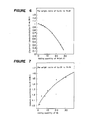
- Figure 7 shows a relationship between the contact resistance and a quantity of Nb added to the alloy for the contact material, wherein the weight ratio between Cu and Cr is fixed at 75:25.
- the graph shows a similar tendency to the electrical conductivity.
- the ordinate in the graph of Figure 7 denotes a ratio when the electrical conductivity value of a conventional alloy consisting of Cu and 25% by weight of Cr is made 1.
- Figure 8 indicates a relationship between the current breaking capacity and an amount of Nb added to the alloy, in which the weight ratio between Cu and Cr is fixed at 75:25. It is seen from this graphical representation that the alloy added with Nb has a remarkably increased current breaking capability in comparison with the conventional alloy (Cu-25% by weight Cr).
- the ordinate in the graph of Figure 8 shows a ratio when the electrical conductivity value of the conventional alloy consisting of Cu and 25 wt.% Cr is made 1.
- the current breaking capacity of the alloy augments. It reaches 1.8 times as high as that of the conventional alloy with the added quantity of Nb of 5% by weight.
- the current breaking capacity decreases conversely.
- Figure 9 shows a relationship between the voltage withstand capability and the adding quantity of Nb.
- the difference in the voltage withstand capability.of the alloy of the invention and the conventional alloy is slight with the added Nb quantity of 3% by weight and below. With increase in its adding quantity, however, the voltage withstand capability is seen to rise.
- Figure 10 indicates a relationship between the electrical conductivity and the weight ratio of Cr to Cu.
- Figure 11 shows a relationship between the current breaking capability and the weight ratio of Cr, when the adding quantity of Nb to the alloy is fixed at 0, 1.3, 5, 10, 20, 30, and 40% by weight, respectively, and the weight ratio of Cr to Cu is varied in each alloy of the abovementioned Nb content.
- the ordinate represents a ratio when the current breaking capacity value of the conventional alloy (Cu-25 wt.% Cr) is made 1, and the abscissa denotes the weight ratio of Cr to Cu.
- the conventional alloy (Cu-Cr binary alloy) indicates a peak in its current breaking capacity with the Cr content being in a range of from 20 to 30% by weight. A similar tendency is observed when the Nb content is fixed at 1 to 5% by weight.
- Figure 12 shows a relationship between the electrical conductivity and the Nb content in the binary alloy of Cu and Nb
- Figure 13 indicates a relationship between the electrical conductivity and the Cr content in the binary alloy of Cu and Cr.
- the alloy of this figure of the Nb content is difficult to be realized for the practical purpose, except for the circuit breaker of a particular use, because such alloy is difficult to be obtained by an ordinary sintering method and, as is apparent from Figure 12, with the Nb content of 40% by weight and above, the electrical conductivity becomes low and the contact resistance becomes high.
- a range of the weight ratio of the constituent elements in the alloy, wherein the current breaking capability remarkably increases (exceeding 1.5 times) in comparison with the conventional alloy should desirably be 1 to 30% by weight of Nb and up to 33% by weight of Cr to Cu.
- the Cu-Cr-Nb alloy obtained by mixing the same constituent elements at the same ratio as mentioned above, shaping the mixture, and sintering the shaped material is excellent in its current breaking capability, if the intermetallic compound of Cr and Nb has been formed in it.
- vacuum circuit breaker obtained from the abovementioned alloy which is added at least one kind of low melting point metals such as Bi, Te, Sb, TI, Pb, Se, Ce and Ca, alloys of these metals, and intermetallic compounds of these metals has the effect of increasing the current breaking capability and the voltage withstand capability same as the abovementioned experimental examples.
- the contact material according to this first embodiment of the present invention is characterized by containing copper as the basic component and, Cr and Nb as the other components, wherein copper, chromium and niobium are distributed therein in the form of a single metal or as at least one kind of a ternary alloy of these metals, a binary alloy of these metals, a ternary intermetallic compound of these metals, a binary intermetallic compound of these metals, and a composite body of these thereby obtaining excellent current breaking. capability and high voltage withstand capability.
- Figure 14 indicates a relationship between the current breaking capacity and the Ti content added to the alloy for the contact material, wherein the Cr content is fixed at 25% by weight, and the Nb content is fixed at 0, 1, 3, 5, 10, 15, and 20% by weight, respectively.
- the ordinate represents a ratio when the current breaking capacity of the conventional alloy (consisting of Cu-25 Cr) is made 1, and the abscissa denotes the adding quantity of Ti.
- a reference letter A indicates the current breaking capacity of the conventional alloy (consisting of Cu-25 Cr).
- the Nb content is 15% by weight, if the Ti content is 0.5% by weight or below, there is no change in the current breaking capability, and, if the Ti content exceeds 0.5% by weight, rather, decrease in current breaking capability takes place. Further, when the Nb content reaches 20% by weight, the current breaking capacity decreases with increase of Ti content. Namely, the effect for improving the current breaking capacity to be derived from addition of Ti is effective when the Nb content is 15% by weight or below. More concretely, when 0.5% by weight of Ti is added with respect to 3% by weight of Nb, the alloy exhibits its current breaking capacity of 1.9 times as large as that of the conventional alloy (consisting of Cu-25 wt.% Cr).
- Figure 15 indicates a relationship between the current breaking capacity and the Nb content added to the alloy for the contact material, wherein the Cr content is fixed at 25% by weight, and the Ti content is fixed at 0, 0.5, 1.0, and 1.5% by weight, respectively.
- the ordinate denotes a ratio when the current breaking capacity of the conventional alloy (consisting of Cu-25 wt.% Cr) is made 1
- the abscissa denotes the adding quantity of Nb.
- it is with 15% by weight or below of Nb added that the increased effect in the current breaking capacity can be observed by the addition of Ti at a rate of 0.5% by weight.
- the adding quantity of Ti is preferably 1% by weight or below.
- the Ti content being in a range of 0.5% by weight or below, there emerges an improved effect in the current breaking capability over the broadest range of the Nb content, i.e., a range of 15% by weight or below.
- ranges of 0.8% by weight or below of Ti and 2 to 7% by weight of Nb are preferably for further improvement in the current breaking capability of the ternary alloy of Cu-Cr-Nb by addition of Ti thereto.
- the present inventors conducted experiments as shown in Figures 14 and 15 by varying the Cr content. With the Cr content in a range of from 10 to 35% by weight, there could be observed improvement in the current breaking capability due to addition of Ti, while, with the Cr content in a range of 10% by weight or less, there took place no change in the current breaking capability even by addition of Ti. Conversely, when the Cr content exceeds 35% by weight, there takes place lowering of the current breaking capability.
- the contact material made of the Cu-Cr-Nb-Ti series alloy containing Cr in a range of from 10 to 35% by weight, Nb in a range of 15% by weight or less, and Ti in a range of 1% by weight or less is not inferior in its contact resistance to the conventional alloy (consisting of Cu-25 wt.% Cr) and is also satisfactory in its voltage withstand capability, which, though not shown in the drawing, have been verified from various experiments.
- the low melting point metals when at least one kind of the low melting point metals, their alloys, their intermetallic compounds, and their oxides is added to the alloy in an amount of 20% by weight and above, the current breaking capability and the voltage withstand capability of the alloy decreased remarkably. Moreover, in the case of the low melting point metal being Ce or Ca, the characteristics of the alloy are somewhat inferior.
- the second embodiment of the present invention is characterized in that the alloy for the contact material consists essentially of copper, 10 to 35% by weight of chromium, 15% by weight or below of niobium, and 1 % by weight or below of titanium. Therefore, the invention has its effect such that the contact material for the vacuum circuit breaker excellent in its current breaking capability and having satisfactory voltage withstand capability can be obtained even if the Nb content is reduced.
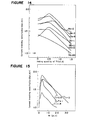
- Figure 16 indicates a relationship between the current breaking capacity and the AI content added to the alloy, in which the Cr content is fixed at 25% by weight and the Nb content is fixed at 0, 1, 5, 10, 15, and 20% by weight, respectively.
- the ordinate denotes a ratio when the current breaking capacity of conventional alloy (Cu-25 wt. % Cr) is made 1
- the abscissa denotes the adding quantity of AI.
- a reference letter A represents the current breaking capacity of the conventional alloy (Cu-25 wt.% Cr).
- Figure 17 indicates a relationship between the current breaking capacity and the quantity of Nb, when the Cr content in the alloy for the contact material is fixed at 25% by weight and the AI content is fixed at 0, 0.6, and 1.0% by weight, respectively.
- the ordinate denotes a ratio when the current breaking capacity of the conventional alloy (consisting of Cu-25 wt.% Cr) is made 1
- the abscissa denotes the adding quantity of Nb.
- it is with 20% by weight or below of the quantity of Nb added that the increased effect in the current breaking capacity can be observed over the broadest range by addition of Nb when the quantity of AI is 0.6% by weight.
- the adding quantity of AI is preferably 1% by weight or below.
- the AI content being in a range of 0.6% by weight or below, there emerges an improved effect in the current breaking capability over the broadest range of the Nb content, i.e., a range of 20% by weight or below.
- ranges of 0.7% by weight or below of AI and 2 to 7% by weight of Nb are preferably for further improvement in the current breaking capability of the ternary alloy of Cu-Cr-Nb by addition of AI thereto:
- the contact material made of the Cu-Cr-Nb-AI series alloy containing Cr in a range of from 10 to 35% by weight, Nb in a range of 20% by weight or below, and AI in a range of 1 % by weight or below is not inferior in its contact resistance to the conventional alloy (consisting of Cu-25 wt.% Cr) and has as good a voltage withstand capability as that of the conventional alloy, which have been verified from various experiments, though not shown in the drawing.
- the low melting point metals when at least one kind of the low melting point metals, their alloys, their intermetallic compounds, and their oxides is added to the alloy in an amount of 20% by weight and above, the current breaking capability and the voltage withstand capability of the alloy decreased remarkably. Moreover, in the case of the low melting point metal being Ce or Ca, the characteristics of the alloy are somewhat inferior.
- the third embodiment of the present invention is characterized in that the alloy for the contact material consists essentially of copper, 10 to 35% by weight of chromium, 20% by weight or below of niobium, and 1% by weight or below of aluminum. Therefore, the present invention has its effect such that the contact material for the vacuum circuit breaker excellent in its current breaking capability and having satisfactory voltage withstand capability can be obtained even if the quantity of Nb is reduced.
- Figure 18 indicates a relationship between the current breaking capacity and the Zr content added to the alloy, in which the Cr content is fixed at 25% by weight and the quantity of Nb is fixed at 0, 1, 3, 5, 10, 15, and 20% by weight, respectively.
- the ordinate represents a ratio when the current breaking capacity of a conventional alloy (Cu-25 wt.% Cr) is made 1, and the abscissa denotes the adding quantity of Zr.
- a reference letter A indicates the current breaking capacity of the conventional alloy (Cu-25 wt.% Cr).
- Figure 19 shows a relationship between the current breaking capacity and the quantity of Nb, when the Cr content in the alloy for the contact material is fixed at 25% by weight and the Zr content is fixed at 0, 0.4, and 0.8% by weight, respectively.
- the ordinate represents a ratio when the current breaking capacity of the conventional alloy (consisting of Cu-25 wt.% Cr) is made 1
- the abscissa represents the adding quantity of Nb.
- it is with 15% by weight or below of the quantity of Nb added that the increased effect in the current breaking capacity can be observed most eminently by addition of Zr, when the quantity of Zr is 0.4% by weight.
- the adding quantity of Zr is preferably 0.8% by weight or below.
- the Zr content being in a range of 0.4% by weight or below, there emerges an improved effect in the current breaking capability over the broadest range of the Nb content, i.e., a range of 15% by weight or below.
- the quantity of Zr be in a range of 0.65% by weight or below and the quantity of Nb be in a range of from 2 to 7% by weight for further improvement in the current breaking capability of the ternary alloy of Cu-Cr-Nb by addition of Zr thereto.
- the present inventors conducted experiments as shown in Figures 18 and 19 by varying the quantity of Cr. With the quantity of Cr being in a range of 10 to 35% by weight, there could be observed improvement in the current breaking capability by the addition of Zr. However, with the quantity of Cr being in a range of 10% by weight or below, there could be seen no change in the current breaking capability even by addition of Zr. Conversely, when the quantity of Cr exceeds 35% by weight, there takes place lowering of the current breaking capability.
- the contact material made of the Cu-Cr-Nb-Zr series alloy containing Cr in a range of from 10 to 35% by weight, Nb in a range of 15% by weight or below, and Zr in a range of 0.8% by weight or below is not inferior in its contact resistance to the conventional alloy (consisting of Cu-25 wt.% Cr) and has as good a voltage withstand capability as that of the conventional alloy, which have been verified from various experiments, though not shown in the drawing.
- the current breaking capability of the alloy decreased remarkably.
- the low melting point metal being Ce or Ca
- the characteristics of the alloy are somewhat inferior.
- the fourth embodiment of the present invention is characterized in that the alloy for the contact material consists essentially of copper, 10 to 35% by weight of chromium, 15% by weight or below of niobium, and 0.8% by weight or below of zirconium. Therefore, the present invention has its effect such that the contact material for the vacuum circuit breaker excellent in its current breaking capability and having satisfactory voltage withstand capability can be obtained, even if the quantity of Nb is reduced.
Landscapes
- High-Tension Arc-Extinguishing Switches Without Spraying Means (AREA)
Claims (16)
Applications Claiming Priority (8)
| Application Number | Priority Date | Filing Date | Title |
|---|---|---|---|
| JP202530/82 | 1982-11-16 | ||
| JP20253082A JPS5991617A (ja) | 1982-11-16 | 1982-11-16 | 真空しや断器用接点 |
| JP7672083A JPS59201334A (ja) | 1983-04-29 | 1983-04-29 | 真空しや断器用接点材料 |
| JP7672283A JPS59201336A (ja) | 1983-04-29 | 1983-04-29 | 真空しや断器用接点材料 |
| JP7672183A JPS59201335A (ja) | 1983-04-29 | 1983-04-29 | 真空しや断器用接点材料 |
| JP76722/83 | 1983-04-29 | ||
| JP76721/83 | 1983-04-29 | ||
| JP76720/83 | 1983-04-29 |
Publications (2)
| Publication Number | Publication Date |
|---|---|
| EP0109088A1 EP0109088A1 (de) | 1984-05-23 |
| EP0109088B1 true EP0109088B1 (de) | 1986-03-19 |
Family
ID=27465970
Family Applications (1)
| Application Number | Title | Priority Date | Filing Date |
|---|---|---|---|
| EP83111417A Expired EP0109088B1 (de) | 1982-11-16 | 1983-11-15 | Kontaktwerkstoff für Vakuumschalter |
Country Status (3)
| Country | Link |
|---|---|
| US (1) | US4575451A (de) |
| EP (1) | EP0109088B1 (de) |
| DE (1) | DE3362624D1 (de) |
Cited By (1)
| Publication number | Priority date | Publication date | Assignee | Title |
|---|---|---|---|---|
| DE4110600A1 (de) * | 1990-04-04 | 1991-10-17 | Hitachi Ltd | Vakuum-leistungsschalter sowie elektrode und elektrodenmaterial fuer einen solchen |
Families Citing this family (16)
| Publication number | Priority date | Publication date | Assignee | Title |
|---|---|---|---|---|
| JPS60172116A (ja) * | 1984-02-16 | 1985-09-05 | 三菱電機株式会社 | 真空しや断器用接点 |
| US4626282A (en) * | 1984-10-30 | 1986-12-02 | Mitsubishi Denki Kabushiki Kaisha | Contact material for vacuum circuit breaker |
| CN1003329B (zh) * | 1984-12-13 | 1989-02-15 | 三菱电机有限公司 | 真空断路器用触头 |
| US4784829A (en) * | 1985-04-30 | 1988-11-15 | Mitsubishi Denki Kabushiki Kaisha | Contact material for vacuum circuit breaker |
| KR900001613B1 (ko) * | 1986-01-10 | 1990-03-17 | 미쯔비시 덴끼 가부시기가이샤 | 진공차단기용 접점재료 |
| JPH0760623B2 (ja) * | 1986-01-21 | 1995-06-28 | 株式会社東芝 | 真空バルブ用接点合金 |
| EP0368860A1 (de) * | 1987-07-28 | 1990-05-23 | Siemens Aktiengesellschaft | Kontaktwerkstoff für vakuumschalter und verfahren zu dessen herstellung |
| JP2768721B2 (ja) * | 1989-03-01 | 1998-06-25 | 株式会社東芝 | 真空バルブ用接点材料 |
| US5252147A (en) * | 1989-06-15 | 1993-10-12 | Iowa State University Research Foundation, Inc. | Modification of surface properties of copper-refractory metal alloys |
| JP2766441B2 (ja) * | 1993-02-02 | 1998-06-18 | 株式会社東芝 | 真空バルブ用接点材料 |
| JP3597544B2 (ja) * | 1993-02-05 | 2004-12-08 | 株式会社東芝 | 真空バルブ用接点材料及びその製造方法 |
| DE19714654A1 (de) * | 1997-04-09 | 1998-10-15 | Abb Patent Gmbh | Vakuumschaltkammer mit einem festen und einem beweglichen Kontaktstück und/oder einem Schirm von denen wenigstens die Kontaktstücke wenigstens teilweise aus Cu/Cr, Cu/CrX oder Cu/CrXY bestehen |
| RU2174563C2 (ru) * | 1999-11-15 | 2001-10-10 | Закрытое акционерное общество "Техпромстрой" | Материал скользящего контакта для электрических машин на основе меди |
| NL1017843C2 (nl) * | 2001-04-12 | 2002-10-22 | Vitronics Soltec B V | Inrichting voor selectief solderen. |
| JP6253494B2 (ja) * | 2014-04-21 | 2017-12-27 | 三菱電機株式会社 | 真空バルブ用接点材料及び真空バルブ |
| EP4681920A1 (de) * | 2024-07-17 | 2026-01-21 | ManVision GmbH & Co. KG | Vorlegierung für am |
Family Cites Families (16)
| Publication number | Priority date | Publication date | Assignee | Title |
|---|---|---|---|---|
| US1375454A (en) * | 1919-09-19 | 1921-04-19 | Hansen Halliburton Mfg Company | Electrical-resistance alloy |
| US2311750A (en) * | 1941-10-17 | 1943-02-23 | Mallory & Co Inc P R | Welding electrode |
| DE1198566B (de) * | 1954-12-20 | 1965-08-12 | Kurt Dies Dr Ing | Verwendung von aushaertbaren und verformungsfaehigen Kupferlegierungen fuer auf Gleitung und Verschleiss beanspruchte Gegenstaende |
| GB1020914A (en) * | 1961-11-10 | 1966-02-23 | Gen Electric | Improvements in vacuum circuit interrupter |
| GB1079013A (en) * | 1964-04-21 | 1967-08-09 | English Electric Co Ltd | Improvements in or relating to contacts and electrodes |
| US3514559A (en) * | 1967-03-27 | 1970-05-26 | Mc Graw Edison Co | Vacuum type circuit interrupter |
| JPS4840384B1 (de) * | 1968-08-26 | 1973-11-30 | ||
| US3627963A (en) * | 1971-03-18 | 1971-12-14 | Wesley N Lindsay | Vacuum interrupter contacts |
| DE2346179A1 (de) * | 1973-09-13 | 1975-06-26 | Siemens Ag | Verbundmetall als kontaktwerkstoff fuer vakuumschalter |
| DE2357333C3 (de) * | 1973-11-16 | 1980-04-03 | Siemens Ag, 1000 Berlin Und 8000 Muenchen | Durchdringungsverbundmetall als Kontaktwerkstoff für Vakuumschalter |
| US4008081A (en) * | 1975-06-24 | 1977-02-15 | Westinghouse Electric Corporation | Method of making vacuum interrupter contact materials |
| US4049426A (en) * | 1976-10-04 | 1977-09-20 | Olin Corporation | Copper-base alloys containing chromium, niobium and zirconium |
| JPS5519710A (en) * | 1978-07-28 | 1980-02-12 | Hitachi Ltd | Vacuum breaker electrode |
| JPS6059691B2 (ja) * | 1979-02-23 | 1985-12-26 | 三菱電機株式会社 | 真空しや断器用接点及びその製造方法 |
| US4378330A (en) * | 1979-03-12 | 1983-03-29 | The United States Of America As Represented By The Department Of Energy | Ductile alloy and process for preparing composite superconducting wire |
| JPS56133442A (en) * | 1980-03-24 | 1981-10-19 | Tanaka Kikinzoku Kogyo Kk | Electrical contact material |
-
1983
- 1983-11-15 DE DE8383111417T patent/DE3362624D1/de not_active Expired
- 1983-11-15 EP EP83111417A patent/EP0109088B1/de not_active Expired
- 1983-11-16 US US06/552,442 patent/US4575451A/en not_active Expired - Lifetime
Cited By (1)
| Publication number | Priority date | Publication date | Assignee | Title |
|---|---|---|---|---|
| DE4110600A1 (de) * | 1990-04-04 | 1991-10-17 | Hitachi Ltd | Vakuum-leistungsschalter sowie elektrode und elektrodenmaterial fuer einen solchen |
Also Published As
| Publication number | Publication date |
|---|---|
| US4575451A (en) | 1986-03-11 |
| DE3362624D1 (en) | 1986-04-24 |
| EP0109088A1 (de) | 1984-05-23 |
Similar Documents
| Publication | Publication Date | Title |
|---|---|---|
| EP0110176B1 (de) | Kontaktwerkstoff für Vakuumschalter | |
| EP0109088B1 (de) | Kontaktwerkstoff für Vakuumschalter | |
| US4486631A (en) | Contact for vacuum circuit breaker | |
| CA1327131C (en) | Electrical contacts for vacuum interrupter devices | |
| US4853184A (en) | Contact material for vacuum interrupter | |
| US5500499A (en) | Contacts material for vacuum valve | |
| EP0126347B2 (de) | Kontaktwerkstoff für Vakuumschalter, Kontaktglied aus diesem Werkstoff, Vakuumschalter und Verwendung des Werkstoffes | |
| JPS59201334A (ja) | 真空しや断器用接点材料 | |
| JPS6336089B2 (de) | ||
| JPH0133011B2 (de) | ||
| JPS6336090B2 (de) | ||
| JPH036211B2 (de) | ||
| JPS59214121A (ja) | 真空しや断器用接点材料 | |
| JPH0313295B2 (de) | ||
| JPH0449734B2 (de) | ||
| JPS6336092B2 (de) | ||
| JPH0449733B2 (de) | ||
| JPS59201335A (ja) | 真空しや断器用接点材料 | |
| JPS59201336A (ja) | 真空しや断器用接点材料 | |
| JPS60170122A (ja) | 真空しや断器用接点材料 | |
| JPH0347931A (ja) | 真空バルブ用接点材料 | |
| JPS59167925A (ja) | 真空しや断器用接点材料 | |
| JPH0241571B2 (de) | ||
| JPH0241572B2 (de) | ||
| JPS59186218A (ja) | 真空しや断器用接点材料 |
Legal Events
| Date | Code | Title | Description |
|---|---|---|---|
| PUAI | Public reference made under article 153(3) epc to a published international application that has entered the european phase |
Free format text: ORIGINAL CODE: 0009012 |
|
| AK | Designated contracting states |
Designated state(s): DE FR GB SE |
|
| 17P | Request for examination filed |
Effective date: 19840511 |
|
| GRAA | (expected) grant |
Free format text: ORIGINAL CODE: 0009210 |
|
| AK | Designated contracting states |
Kind code of ref document: B1 Designated state(s): DE FR GB SE |
|
| REF | Corresponds to: |
Ref document number: 3362624 Country of ref document: DE Date of ref document: 19860424 |
|
| ET | Fr: translation filed | ||
| PLBE | No opposition filed within time limit |
Free format text: ORIGINAL CODE: 0009261 |
|
| STAA | Information on the status of an ep patent application or granted ep patent |
Free format text: STATUS: NO OPPOSITION FILED WITHIN TIME LIMIT |
|
| 26N | No opposition filed | ||
| EAL | Se: european patent in force in sweden |
Ref document number: 83111417.8 |
|
| PGFP | Annual fee paid to national office [announced via postgrant information from national office to epo] |
Ref country code: SE Payment date: 19951116 Year of fee payment: 13 |
|
| REG | Reference to a national code |
Ref country code: GB Ref legal event code: 746 Effective date: 19951026 |
|
| REG | Reference to a national code |
Ref country code: FR Ref legal event code: D6 |
|
| PG25 | Lapsed in a contracting state [announced via postgrant information from national office to epo] |
Ref country code: SE Effective date: 19961116 |
|
| EUG | Se: european patent has lapsed |
Ref document number: 83111417.8 |
|
| PGFP | Annual fee paid to national office [announced via postgrant information from national office to epo] |
Ref country code: FR Payment date: 20011113 Year of fee payment: 19 |
|
| PGFP | Annual fee paid to national office [announced via postgrant information from national office to epo] |
Ref country code: GB Payment date: 20011114 Year of fee payment: 19 |
|
| PGFP | Annual fee paid to national office [announced via postgrant information from national office to epo] |
Ref country code: DE Payment date: 20011203 Year of fee payment: 19 |
|
| REG | Reference to a national code |
Ref country code: GB Ref legal event code: IF02 |
|
| PG25 | Lapsed in a contracting state [announced via postgrant information from national office to epo] |
Ref country code: GB Free format text: LAPSE BECAUSE OF NON-PAYMENT OF DUE FEES Effective date: 20021115 |
|
| PG25 | Lapsed in a contracting state [announced via postgrant information from national office to epo] |
Ref country code: DE Free format text: LAPSE BECAUSE OF NON-PAYMENT OF DUE FEES Effective date: 20030603 |
|
| GBPC | Gb: european patent ceased through non-payment of renewal fee | ||
| PG25 | Lapsed in a contracting state [announced via postgrant information from national office to epo] |
Ref country code: FR Free format text: LAPSE BECAUSE OF NON-PAYMENT OF DUE FEES Effective date: 20030731 |
|
| REG | Reference to a national code |
Ref country code: FR Ref legal event code: ST |