EP0109332A1 - Anordnung zum Empfangen von Funksprüchen mit biphasenartigen Signalen - Google Patents
Anordnung zum Empfangen von Funksprüchen mit biphasenartigen Signalen Download PDFInfo
- Publication number
- EP0109332A1 EP0109332A1 EP19830402126 EP83402126A EP0109332A1 EP 0109332 A1 EP0109332 A1 EP 0109332A1 EP 19830402126 EP19830402126 EP 19830402126 EP 83402126 A EP83402126 A EP 83402126A EP 0109332 A1 EP0109332 A1 EP 0109332A1
- Authority
- EP
- European Patent Office
- Prior art keywords
- bits
- loop
- input
- phase
- channel
- Prior art date
- Legal status (The legal status is an assumption and is not a legal conclusion. Google has not performed a legal analysis and makes no representation as to the accuracy of the status listed.)
- Granted
Links
- 238000001514 detection method Methods 0.000 claims abstract description 11
- 238000000034 method Methods 0.000 claims abstract 7
- 230000001360 synchronised effect Effects 0.000 claims abstract 2
- 238000010586 diagram Methods 0.000 claims description 9
- 230000010363 phase shift Effects 0.000 claims description 7
- 230000006870 function Effects 0.000 claims description 4
- 238000005314 correlation function Methods 0.000 claims 1
- 235000021183 entrée Nutrition 0.000 description 6
- 238000009434 installation Methods 0.000 description 4
- 240000008042 Zea mays Species 0.000 description 3
- 230000010354 integration Effects 0.000 description 2
- 230000003595 spectral effect Effects 0.000 description 2
- 230000006978 adaptation Effects 0.000 description 1
- 230000005540 biological transmission Effects 0.000 description 1
- 230000001427 coherent effect Effects 0.000 description 1
- 230000007423 decrease Effects 0.000 description 1
- 230000000694 effects Effects 0.000 description 1
- 230000010355 oscillation Effects 0.000 description 1
- 230000001052 transient effect Effects 0.000 description 1
Images

Classifications
-
- H—ELECTRICITY
- H04—ELECTRIC COMMUNICATION TECHNIQUE
- H04L—TRANSMISSION OF DIGITAL INFORMATION, e.g. TELEGRAPHIC COMMUNICATION
- H04L7/00—Arrangements for synchronising receiver with transmitter
- H04L7/04—Speed or phase control by synchronisation signals
- H04L7/041—Speed or phase control by synchronisation signals using special codes as synchronising signal
- H04L7/046—Speed or phase control by synchronisation signals using special codes as synchronising signal using a dotting sequence
-
- H—ELECTRICITY
- H04—ELECTRIC COMMUNICATION TECHNIQUE
- H04L—TRANSMISSION OF DIGITAL INFORMATION, e.g. TELEGRAPHIC COMMUNICATION
- H04L25/00—Baseband systems
- H04L25/38—Synchronous or start-stop systems, e.g. for Baudot code
- H04L25/40—Transmitting circuits; Receiving circuits
- H04L25/49—Transmitting circuits; Receiving circuits using code conversion at the transmitter; using predistortion; using insertion of idle bits for obtaining a desired frequency spectrum; using three or more amplitude levels ; Baseband coding techniques specific to data transmission systems
- H04L25/4904—Transmitting circuits; Receiving circuits using code conversion at the transmitter; using predistortion; using insertion of idle bits for obtaining a desired frequency spectrum; using three or more amplitude levels ; Baseband coding techniques specific to data transmission systems using self-synchronising codes, e.g. split-phase codes
-
- H—ELECTRICITY
- H04—ELECTRIC COMMUNICATION TECHNIQUE
- H04L—TRANSMISSION OF DIGITAL INFORMATION, e.g. TELEGRAPHIC COMMUNICATION
- H04L7/00—Arrangements for synchronising receiver with transmitter
- H04L7/02—Speed or phase control by the received code signals, the signals containing no special synchronisation information
- H04L7/033—Speed or phase control by the received code signals, the signals containing no special synchronisation information using the transitions of the received signal to control the phase of the synchronising-signal-generating means, e.g. using a phase-locked loop
-
- H—ELECTRICITY
- H04—ELECTRIC COMMUNICATION TECHNIQUE
- H04L—TRANSMISSION OF DIGITAL INFORMATION, e.g. TELEGRAPHIC COMMUNICATION
- H04L7/00—Arrangements for synchronising receiver with transmitter
- H04L7/04—Speed or phase control by synchronisation signals
- H04L7/10—Arrangements for initial synchronisation
Definitions
- the invention relates to an apparatus for the reception of radio messages consisting of a succession of "digital" signals such as those used for the transmission between beacons, on the ground or at sea, and one or more terrestrial surveillance satellites, for example for help rescue people at risk.
- the frequency of the signals or bits constituting the messages transmitted by a beacon varies over time, as well as their carrier frequency.
- the content of a message can vary, in particular from a message sent by one tag to a message sent by another tag. Phase detection is made more difficult.
- the present invention relates to a receiver of the type defined above which does not use this additional loop, which is thus of a simpler and more economical constitution while ensuring synchronization at the various stages of operation under conditions at least equivalent to those of previously known devices.
- the subject of the invention is therefore a device for receiving a radio message consisting of a succession of digital or digital signals representative of "O" and "1", comprising a first part or acquisition part or preamble constituted by a succession of identical signals or bits, "O” or “1", in particular of the biphase type, the message being read by recognizing the bits or detection using a phase correlator further attacked from rectangular reference signals or clock signals generated at the receiver, the frequency and phase of said reference signals being controlled from that of the bits received in the acquisition period by phase comparison in an error voltage control loop, characterized in that the control loop for obtaining the attachment during the acquisition period is that which is used to control the phase of the reference signals for the duration of the significant part of the message, owing to the fact that the error voltage delivered by the loop is reversed upon reception of a bit of type opposite to that of the acquisition bits, the loop bandwidth is preferably made narrower at the end of the acquisition time.
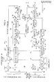
- the radio message received at the satellite is applied by input 31 to the device according to the invention.
- the message is for example of the biphase type, that is to say constituted by a succession of bits "0" and bits "1" as shown in FIG. 2-1, in a significant order of the content of the message. Of course, most of the time, the message is affected by noise.
- the message comprises a first part, or acquisition part, constituted by a succession of identical bits which, in a specification, are bits "1", fifteen in number, forming the preamble of a message where the bits follow one another at the frequency of 400 Hz.
- the input 31 is divided into two branches 32 and 33, the branch 32 being the input of a bit detector 34 and the branch 33 the input of a synchronizer 35.
- the bit detector 34 comprises a correlator 36 constituted by a multiplier 37, one input 38 of which is the end of the channel 32 and the other input 39 of which applies reference signals to it.
- the multiplier 37 is connected by a circuit 41 to an integrator 42, the operation of which is controlled by a control logic 44 so as to achieve integration between time 0 and time T, T being the period of the reference signals.
- the integrator 42 is connected by a circuit 45 to a memory 46, which can be reset to zero by a circuit 47 originating from the control logic 44.
- the output 48 of the memory 46 is divided along a first channel 49 constituting the input of a decision-making device 51 and a second channel 52.
- the decision-making device 51 supplies a positive or negative voltage at its output 53 depending on whether a "1" or an "O" is applied to its input 49.
- the circuit 53 is connected by an interface device 55 to the output 54 going to the rest of the installation.
- Channel 52 leads to the input 56 of a second integrator 57 controlled on the other hand for its reset to zero by a second input 58 connected to the general management of the installation and which intervenes when it is suitable for receiving the message carrying wave.
- the integrator 57 is connected by a circuit 59 to a second decision-making device 61, to a second input 62 to which a voltage of a predetermined value is applied, a decision signal being supplied to the output 63 of the device 61 if the voltage at the input 59 is greater than said value.
- the output 63 is connected to a latch device 64 with a reset input 113,. via an interface 65, the output 66 of the latch device 64 dividing along a first channel 67 and a second channel 68.
- the channel 67 is connected to the general management and embedded therein said signal, or status.
- Channel 68 applies the status to a first input 71 of an AND gate 72 whose other input 73 is connected to output 74 of a logic inverter 75 whose input 76 is connected to channel 54.
- Output 77 of the AND gate 72 controls a switch 78, the condition of which is shown diagrammatically by a movable contact 79 suitable for cooperating either with a first fixed contact 81 or else a second fixed contact 82.
- the contacts 81 and 82 are part of a loop servo control 83, the contact 81 being connected directly to the output 84 of a memory 85 forming part of the loop while the contact 82 is connected to the said output 84 by a voltage reversing device 86, comprising an amplifier 87 and two resistances 88 and 89.
- the memory 85 is connected by a circuit 91 to an integrator 92 whose integration time is equal to T, under the effect of controlling a circuit 93 originating from the control logic 44.
- the integrator 92 receives the signals from a multiplier 94 of which an input 95 is part of the branch 33, which thus applies to the multiplier 94 the bits received, and whose other input 96 receives reference signals, by its connection to the output 97 of the logic 44, whose circuits are part of the control loop 83.
- the input 39 applies reference signals to the first multiplier 37 by its connection to the control logic 44 by a circuit 98, which includes a device 99 for phase shift of ⁇ / 2.
- the control loop 83 includes a third memory 101, an input 102 of which is connected to the switch 78 and of which another input 103 is connected to the control logic 44 by a circuit 104.
- the memory 101 is followed, in the loop, by a loop filter 105, whose output 106 controls, by the value of the voltage which it applies to it, or error voltage, the frequency of the oscillations supplied by an OCT oscillator 107 connected to the control logic 44 forming part of the loop by a circuit 108.
- the signal shown in Figure 2.5 is that which is applied to the input 56 of the integrator 57.
- the voltage present at the output 59 of the integrator 57 gradually increases in the case where the signal applied to its input 56 is same polarity, for example during the acquisition phase where the bits at the input of the device are all "1" bits.
- a signal appears at the output 63, to which corresponds, after adaptation by the interface 65 , a signal or "status" for attachment to the output 66 of the lock 64 and which is present on the channel 67 and on the channel 68.
- the bits arriving at the input 31 are further applied by the input 95 to the servo loop 83, which causes the phase comparator constituted by the multiplier 94, the integrator 92 and the memory to appear. 85, an error voltage controlling the oscillator 107 so as to ensure the synchronization of the clock signals, supplied at the output 97 of the loop, with the input bits.
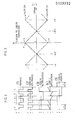
- the operating diagram of the phase comparator is that shown in solid line in FIG. 3, where we have brought in ordered the voltage V at the output 84 of the memory device 85 and on the abscissa the phase shift ⁇ between the bits at the input 31 and the clock signals.
- the voltage at the output 84 is represented by the point a, for example at + 1 volt. This voltage decreases according to a linear law for a phase shift in one direction or the other, to reach the value 0 when the offset is equal to + or - .
- the phase shift increases, the voltage V becomes negative, reaching dre the value -1 volt for an offset equal to ⁇ II.
- the dashed line is a similar diagram, but when the signals arriving at input 31 are bits 0.
- phase comparator comprising the multiplier 94, the integrator 92 and the memory device 85 forming part of a conventional servo loop, it is thus possible, by using identical bits during the acquisition phase, or preamble, obtain the phase shift of the reference signals in the direction which brings them in phase with the bits received, the servo loop then retaining this setting in phase. There is thus obtained, by the detector 34, a coherent detection of the signals received.
- the operation of the servo loop taking into account the properties of the phase comparator used, also tends to reduce the error voltage to zero and, consequently, operate the phase comparator around its zero point, therefore at 90 ° relative to the input bits.
- the residual disturbances at the bit rate are very low, theoretically zero, which allows the use of a sufficiently wide bandwidth to acquire the phase of the signal received in less than 15 bits with a frequency of 400 Hz.
- Synchronizer 35 thus functions like a conventional "sampled" phase loop, when the switching tor 78 is in the condition shown, which is the case in particular during the attachment preamble.
- the AND gate 72 is made operational by its application on the input 71, which translates the fact that the device is suitable for receiving the significant part of the message. .
- the condition of the servo loop 83 is not modified. But when it is a "0" bit which reaches input 31, a signal is also applied to input 73, via the logic inverter 75, and the switch 78 intervenes in the control loop the voltage inverter 86.
- the control loop 83 continues to function satisfactorily to maintain the timing in phase of the clock signals introduced into the multiplier 37 with the input bits.
- the memory 101 which acts as a delay line, takes into account the error information after the switching has been carried out, which avoids transient disturbances in the loop.
- the invention provides for reducing the bandwidth width of the loop 83 in the "tracking", that is to say during the processing of the significant part of the message, which is advantageous for the processing of bits of input with extremely low signal-to-noise ratio.
- the probability of bit error is better than 10 -5 under the conditions defined above.
- FIG. 4 shows a diagram of an apparatus according to the invention for a digital embodiment.
- the input 201 of the two-phase signals (marred by noise) is applied to an analog / digital converter 202 whose output 203 is divided into two channels 204 and 205 transmitting the information of absolute value of the signals.
- Line 204 is the input of a channel 206 comprising the bit detector and line 205 is the input of a channel 207 comprising the synchronizer.
- Channel 206 includes an adder-subtractor 208 followed by a memory register 209 whose output 211 is connected, on the one hand, to a decision-making device 212 supplying at its output 213 information> 0 or l information ⁇ 0 depending on the type of bit received.
- the memory register 209 is also connected to the input 214 of an accumulator 215 with reset input 216 216.
- the output 217 of the accumulator 215 is connected to a decision-making device 218 causing a decision signal to appear when it leaves 219 when: N being the spectral density of the noise, the reference value a being introduced by the input 221.
- the appearance of a signal at output 219 triggers the operation of a lock 222 having a reset input 223, the output 224 of the lock constituting the latching status
- Channel 207 is part of a control loop 231 which includes an adder-subtractor 232 controlled by a second input 233, the adder subtractor 208 from channel 206 being likewise controlled by an input 234, inputs 233 and 234 being connected to the outputs of exclusive OR doors 235 and 236 respectively, of which the first two inputs 237 and 238 are connected to the circuit 239, coming from the analog / digital converter 202 and carrying the sign.
- the other inputs of doors 235 and 236 are connected by circuits 241 and 242 to a control logic 243, a phase shift of r / 2 existing between the signals delivered to said outputs, so that the phases of stalling respectively on the channels 206 and 207 differ from each other by 2.
- the control logic 243 is part of the control loop 231. It is connected to the output 244 of an OCN numerically controlled oscillator 245, which is controlled from a digital loop filter 246 receiving by a circuit 247 the information from a memory register 248. The latter receives at its end 249 phase error information present in a circuit 251 from a memory register 252, the input 253 of which is connected to the adder-subtractor 232.
- phase error information present on the circuit 251 is applied to the input of an exclusive OR gate 254 whose other input 255 is connected to the output of an AND gate 256 of which an input 257 is connected by a circuit 258 to the output 224 of the lock device 222 and the other input 259 of which is connected to the output 213 of the decision-making device 212.
- input signals are shown with a rectangular configuration, but the invention also applies to signals of different configuration, for example rounded, such as pre-filtered two-phase signals.
Landscapes
- Engineering & Computer Science (AREA)
- Computer Networks & Wireless Communication (AREA)
- Signal Processing (AREA)
- Physics & Mathematics (AREA)
- Spectroscopy & Molecular Physics (AREA)
- Stabilization Of Oscillater, Synchronisation, Frequency Synthesizers (AREA)
- Synchronisation In Digital Transmission Systems (AREA)
Applications Claiming Priority (2)
| Application Number | Priority Date | Filing Date | Title |
|---|---|---|---|
| FR8218280 | 1982-10-29 | ||
| FR8218280A FR2535554B1 (fr) | 1982-10-29 | 1982-10-29 | Procede et appareil pour la reception de messages radio a signaux de type biphase |
Publications (2)
| Publication Number | Publication Date |
|---|---|
| EP0109332A1 true EP0109332A1 (de) | 1984-05-23 |
| EP0109332B1 EP0109332B1 (de) | 1987-05-06 |
Family
ID=9278792
Family Applications (1)
| Application Number | Title | Priority Date | Filing Date |
|---|---|---|---|
| EP19830402126 Expired EP0109332B1 (de) | 1982-10-29 | 1983-10-28 | Anordnung zum Empfangen von Funksprüchen mit biphasenartigen Signalen |
Country Status (3)
| Country | Link |
|---|---|
| EP (1) | EP0109332B1 (de) |
| DE (1) | DE3371451D1 (de) |
| FR (1) | FR2535554B1 (de) |
Cited By (4)
| Publication number | Priority date | Publication date | Assignee | Title |
|---|---|---|---|---|
| EP0173298A3 (en) * | 1984-08-27 | 1987-11-04 | Nec Corporation | Demodulation device for multiphase psk or multilevel qam carrier wave |
| FR2611395A1 (fr) * | 1987-02-26 | 1988-09-02 | Plessey Overseas | Systeme de recuperation de donnees et de signaux d'horloge en code manchester |
| GB2216366A (en) * | 1988-02-26 | 1989-10-04 | Silicon General Inc | Timing generator |
| US5329558A (en) * | 1991-04-12 | 1994-07-12 | Telefonaktiebolaget L M Ericsson | Method of synchronizing a radio receiver with an incoming radio signal |
Citations (4)
| Publication number | Priority date | Publication date | Assignee | Title |
|---|---|---|---|---|
| US3766315A (en) * | 1970-09-11 | 1973-10-16 | Nasa | Method and apparatus for a single channel digital communications system |
| US3806816A (en) * | 1972-11-08 | 1974-04-23 | Nasa | Pulse code modulated signal synchronizer |
| FR2281675A1 (fr) * | 1974-08-06 | 1976-03-05 | Dassault Electronique | Dispositif pour la reconnaissance d'informations numeriques d'un message binaire module en phase |
| WO1982002985A1 (en) * | 1981-02-27 | 1982-09-02 | Corp Sperry | Biphase detector |
-
1982
- 1982-10-29 FR FR8218280A patent/FR2535554B1/fr not_active Expired
-
1983
- 1983-10-28 DE DE8383402126T patent/DE3371451D1/de not_active Expired
- 1983-10-28 EP EP19830402126 patent/EP0109332B1/de not_active Expired
Patent Citations (4)
| Publication number | Priority date | Publication date | Assignee | Title |
|---|---|---|---|---|
| US3766315A (en) * | 1970-09-11 | 1973-10-16 | Nasa | Method and apparatus for a single channel digital communications system |
| US3806816A (en) * | 1972-11-08 | 1974-04-23 | Nasa | Pulse code modulated signal synchronizer |
| FR2281675A1 (fr) * | 1974-08-06 | 1976-03-05 | Dassault Electronique | Dispositif pour la reconnaissance d'informations numeriques d'un message binaire module en phase |
| WO1982002985A1 (en) * | 1981-02-27 | 1982-09-02 | Corp Sperry | Biphase detector |
Non-Patent Citations (1)
| Title |
|---|
| PROCEEDINGS OF 30th ANNUAL CONFERENCE OF THE IEEE VEHICULAR TECHNOLOGY SOCIETY, INTERNATIONAL CONFERENCE ON TRANSPORTATION ELECTRONICS, 15-17 septembre 1980, Dearborn, Michigan, IEEE cat. no. 80CH1601-4, pages 1-8(E-25), Bohn Printing Company, New York, US * |
Cited By (6)
| Publication number | Priority date | Publication date | Assignee | Title |
|---|---|---|---|---|
| EP0173298A3 (en) * | 1984-08-27 | 1987-11-04 | Nec Corporation | Demodulation device for multiphase psk or multilevel qam carrier wave |
| FR2611395A1 (fr) * | 1987-02-26 | 1988-09-02 | Plessey Overseas | Systeme de recuperation de donnees et de signaux d'horloge en code manchester |
| GB2216366A (en) * | 1988-02-26 | 1989-10-04 | Silicon General Inc | Timing generator |
| US4933955A (en) * | 1988-02-26 | 1990-06-12 | Silicon General, Inc. | Timing generator |
| GB2216366B (en) * | 1988-02-26 | 1992-04-22 | Silicon General Inc | Timing generator |
| US5329558A (en) * | 1991-04-12 | 1994-07-12 | Telefonaktiebolaget L M Ericsson | Method of synchronizing a radio receiver with an incoming radio signal |
Also Published As
| Publication number | Publication date |
|---|---|
| DE3371451D1 (en) | 1987-06-11 |
| FR2535554A1 (fr) | 1984-05-04 |
| EP0109332B1 (de) | 1987-05-06 |
| FR2535554B1 (fr) | 1986-04-11 |
Similar Documents
| Publication | Publication Date | Title |
|---|---|---|
| EP0036084B1 (de) | Verfahren und Vorrichtung zum Steuern der Beginneinstellung des Taktgebers eines Empfängers für synchrone Daten | |
| EP0178720B1 (de) | Einrichtung zum Empfang von digitalen Daten mit einer adaptiven Taktrückgewinnungsschaltung | |
| EP0530107B1 (de) | PSK-Demodulator mit Korrektur im Basisband für Phasen- oder Frequenzfehler | |
| EP0192061A1 (de) | Einrichtung zur automatischen Verstärkungsregelung eines T.D.M.A.-Empfängers | |
| EP1298812B1 (de) | Verfahren und Anordnung zur Dekodierung eines eintreffenden Ultra-Breitband Impulssignals, insbesondere für ein drahtloses Kommunikationssystem | |
| EP0013343A1 (de) | Verfahren und Vorrichtung zur Auffindung einer Pseudo-Zufallsfolge von 0 Grad- und 180 Grad-Phasenänderungen der Trägerwelle in einem Datenempfänger | |
| EP0194902A1 (de) | Verfahren und Einrichtung zur Spreizbandübertragung, insbesondere zur Informationsübertragung auf ein elektrisches Energieverteilungsnetz | |
| FR2533095A1 (fr) | Procede et dispositif de demodulation d'une onde porteuse modulee en phase par une onde sous-porteuse qui est modulee en deplacement de phase par des signaux en bande de base | |
| EP0099814B1 (de) | Für Funkverbindungen hoher Frequenz in gestörtem Umfeld ausgelegte Einrichtung zur Wiedergewinnung der Taktfrequenz | |
| FR2736231A1 (fr) | Systeme de communication numerique comportant un recepteur dote d'un dispositif de recuperation de rythme | |
| EP0012884B1 (de) | Verfahren und Vorrichtung zur Auffindung einer Pseudo-Zufallsfolge zweier Symbole in einem Datenempfänger, welcher eine Doppelzeitenbandmodulation mit Quadraturträgern verwendet | |
| EP1298811A1 (de) | Verfahren und Gerät zur Impulsdetektierung in einem empfangenen Ultrabreitbandsignal | |
| EP0109332B1 (de) | Anordnung zum Empfangen von Funksprüchen mit biphasenartigen Signalen | |
| EP0018242A1 (de) | Im Zeitmultiplex auf mehreren Kanälen arbeitendes Verfahren und Vorrichtung zur stochastischen Demodulation phasensprungmodulierter Signale | |
| EP0018256B1 (de) | Sender-Empfänger mit automatischer Steuerung der Sende-Empfangsumschaltung und Fernmeldenetz, welches einen solchen Sender-Empfänger enthält | |
| US4241454A (en) | Hard limiting acquisition technique for PSK carrier detector | |
| CA1312657C (fr) | Dispositif de synchronisation en modulation de phase a quatre etats decalee | |
| EP0094040A2 (de) | System zur synchronen Datenübertragung mit Hilfe eines amplitudenmodulierten Trägers konstanter Hüllkurve | |
| EP0905946B1 (de) | Reglung der Abtastung von Biphasensignalen | |
| FR2764147A1 (fr) | Procede et dispositif de recuperation de synchronisation sur un signal transmis a un recepteur de telephone mobile | |
| EP0632610A1 (de) | Einrichtung zur Erkennung von Einzewörtern in einem BPSK-TDMA-System | |
| EP0737868B1 (de) | Verzögerungsregelschleife für GPS Empfänger | |
| EP0246135A1 (de) | Phasen- und Frequenzdetektor und seine Anwendung in einer Phasenregelschleife | |
| CA1303152C (fr) | Dispositif de demodulation de phase et son application a un systeme d'atterissage de type mls | |
| CA2057942C (fr) | Systeme recepteur pour le traitement de signaux recus sur des voies de diversite |
Legal Events
| Date | Code | Title | Description |
|---|---|---|---|
| PUAI | Public reference made under article 153(3) epc to a published international application that has entered the european phase |
Free format text: ORIGINAL CODE: 0009012 |
|
| AK | Designated contracting states |
Designated state(s): BE DE GB IT LU NL |
|
| 17P | Request for examination filed |
Effective date: 19840906 |
|
| GRAA | (expected) grant |
Free format text: ORIGINAL CODE: 0009210 |
|
| AK | Designated contracting states |
Kind code of ref document: B1 Designated state(s): BE DE GB IT LU NL |
|
| REF | Corresponds to: |
Ref document number: 3371451 Country of ref document: DE Date of ref document: 19870611 |
|
| ITF | It: translation for a ep patent filed | ||
| PG25 | Lapsed in a contracting state [announced via postgrant information from national office to epo] |
Ref country code: LU Free format text: LAPSE BECAUSE OF NON-PAYMENT OF DUE FEES Effective date: 19871031 |
|
| PLBE | No opposition filed within time limit |
Free format text: ORIGINAL CODE: 0009261 |
|
| STAA | Information on the status of an ep patent application or granted ep patent |
Free format text: STATUS: NO OPPOSITION FILED WITHIN TIME LIMIT |
|
| 26N | No opposition filed | ||
| ITTA | It: last paid annual fee | ||
| NLT1 | Nl: modifications of names registered in virtue of documents presented to the patent office pursuant to art. 16 a, paragraph 1 |
Owner name: DASSAULT ELECTRONIQUE TE ST.-CLOUD, FRANKRIJK. |
|
| ITPR | It: changes in ownership of a european patent |
Owner name: CAMBIO RAGIONE SOCIALE;DASSAULT ELECTRONIQUE |
|
| PGFP | Annual fee paid to national office [announced via postgrant information from national office to epo] |
Ref country code: BE Payment date: 19971028 Year of fee payment: 15 |
|
| PGFP | Annual fee paid to national office [announced via postgrant information from national office to epo] |
Ref country code: NL Payment date: 19971031 Year of fee payment: 15 |
|
| PGFP | Annual fee paid to national office [announced via postgrant information from national office to epo] |
Ref country code: DE Payment date: 19971125 Year of fee payment: 15 |
|
| PGFP | Annual fee paid to national office [announced via postgrant information from national office to epo] |
Ref country code: GB Payment date: 19981013 Year of fee payment: 16 |
|
| PG25 | Lapsed in a contracting state [announced via postgrant information from national office to epo] |
Ref country code: BE Free format text: LAPSE BECAUSE OF NON-PAYMENT OF DUE FEES Effective date: 19981031 |
|
| BERE | Be: lapsed |
Owner name: DASSAULT ELECTRONIQUE Effective date: 19981031 |
|
| PG25 | Lapsed in a contracting state [announced via postgrant information from national office to epo] |
Ref country code: NL Free format text: LAPSE BECAUSE OF NON-PAYMENT OF DUE FEES Effective date: 19990501 |
|
| NLV4 | Nl: lapsed or anulled due to non-payment of the annual fee |
Effective date: 19990501 |
|
| PG25 | Lapsed in a contracting state [announced via postgrant information from national office to epo] |
Ref country code: DE Free format text: LAPSE BECAUSE OF NON-PAYMENT OF DUE FEES Effective date: 19990803 |
|
| PG25 | Lapsed in a contracting state [announced via postgrant information from national office to epo] |
Ref country code: GB Free format text: LAPSE BECAUSE OF NON-PAYMENT OF DUE FEES Effective date: 19991028 |
|
| GBPC | Gb: european patent ceased through non-payment of renewal fee |
Effective date: 19991028 |