EP0109852A2 - Dispositif d'affichage - Google Patents
Dispositif d'affichage Download PDFInfo
- Publication number
- EP0109852A2 EP0109852A2 EP83307108A EP83307108A EP0109852A2 EP 0109852 A2 EP0109852 A2 EP 0109852A2 EP 83307108 A EP83307108 A EP 83307108A EP 83307108 A EP83307108 A EP 83307108A EP 0109852 A2 EP0109852 A2 EP 0109852A2
- Authority
- EP
- European Patent Office
- Prior art keywords
- display device
- layers
- electrically conductive
- layer
- conductive material
- Prior art date
- Legal status (The legal status is an assumption and is not a legal conclusion. Google has not performed a legal analysis and makes no representation as to the accuracy of the status listed.)
- Withdrawn
Links
Images
Classifications
-
- B—PERFORMING OPERATIONS; TRANSPORTING
- B32—LAYERED PRODUCTS
- B32B—LAYERED PRODUCTS, i.e. PRODUCTS BUILT-UP OF STRATA OF FLAT OR NON-FLAT, e.g. CELLULAR OR HONEYCOMB, FORM
- B32B15/00—Layered products comprising a layer of metal
- B32B15/04—Layered products comprising a layer of metal comprising metal as the main or only constituent of a layer, which is next to another layer of the same or of a different material
- B32B15/08—Layered products comprising a layer of metal comprising metal as the main or only constituent of a layer, which is next to another layer of the same or of a different material of synthetic resin
-
- B—PERFORMING OPERATIONS; TRANSPORTING
- B32—LAYERED PRODUCTS
- B32B—LAYERED PRODUCTS, i.e. PRODUCTS BUILT-UP OF STRATA OF FLAT OR NON-FLAT, e.g. CELLULAR OR HONEYCOMB, FORM
- B32B7/00—Layered products characterised by the relation between layers; Layered products characterised by the relative orientation of features between layers, or by the relative values of a measurable parameter between layers, i.e. products comprising layers having different physical, chemical or physicochemical properties; Layered products characterised by the interconnection of layers
- B32B7/04—Interconnection of layers
- B32B7/12—Interconnection of layers using interposed adhesives or interposed materials with bonding properties
-
- B—PERFORMING OPERATIONS; TRANSPORTING
- B32—LAYERED PRODUCTS
- B32B—LAYERED PRODUCTS, i.e. PRODUCTS BUILT-UP OF STRATA OF FLAT OR NON-FLAT, e.g. CELLULAR OR HONEYCOMB, FORM
- B32B9/00—Layered products comprising a layer of a particular substance not covered by groups B32B11/00 - B32B29/00
- B32B9/02—Layered products comprising a layer of a particular substance not covered by groups B32B11/00 - B32B29/00 comprising animal or vegetable substances, e.g. cork, bamboo, starch
-
- B—PERFORMING OPERATIONS; TRANSPORTING
- B32—LAYERED PRODUCTS
- B32B—LAYERED PRODUCTS, i.e. PRODUCTS BUILT-UP OF STRATA OF FLAT OR NON-FLAT, e.g. CELLULAR OR HONEYCOMB, FORM
- B32B9/00—Layered products comprising a layer of a particular substance not covered by groups B32B11/00 - B32B29/00
- B32B9/04—Layered products comprising a layer of a particular substance not covered by groups B32B11/00 - B32B29/00 comprising such particular substance as the main or only constituent of a layer, which is next to another layer of the same or of a different material
- B32B9/041—Layered products comprising a layer of a particular substance not covered by groups B32B11/00 - B32B29/00 comprising such particular substance as the main or only constituent of a layer, which is next to another layer of the same or of a different material of metal
-
- G—PHYSICS
- G09—EDUCATION; CRYPTOGRAPHY; DISPLAY; ADVERTISING; SEALS
- G09F—DISPLAYING; ADVERTISING; SIGNS; LABELS OR NAME-PLATES; SEALS
- G09F13/00—Illuminated signs; Luminous advertising
- G09F13/28—Signs formed by filament-type lamp
-
- B—PERFORMING OPERATIONS; TRANSPORTING
- B32—LAYERED PRODUCTS
- B32B—LAYERED PRODUCTS, i.e. PRODUCTS BUILT-UP OF STRATA OF FLAT OR NON-FLAT, e.g. CELLULAR OR HONEYCOMB, FORM
- B32B2307/00—Properties of the layers or laminate
- B32B2307/20—Properties of the layers or laminate having particular electrical or magnetic properties, e.g. piezoelectric
- B32B2307/202—Conductive
-
- B—PERFORMING OPERATIONS; TRANSPORTING
- B32—LAYERED PRODUCTS
- B32B—LAYERED PRODUCTS, i.e. PRODUCTS BUILT-UP OF STRATA OF FLAT OR NON-FLAT, e.g. CELLULAR OR HONEYCOMB, FORM
- B32B2307/00—Properties of the layers or laminate
- B32B2307/20—Properties of the layers or laminate having particular electrical or magnetic properties, e.g. piezoelectric
- B32B2307/206—Insulating
-
- B—PERFORMING OPERATIONS; TRANSPORTING
- B32—LAYERED PRODUCTS
- B32B—LAYERED PRODUCTS, i.e. PRODUCTS BUILT-UP OF STRATA OF FLAT OR NON-FLAT, e.g. CELLULAR OR HONEYCOMB, FORM
- B32B2307/00—Properties of the layers or laminate
- B32B2307/50—Properties of the layers or laminate having particular mechanical properties
- B32B2307/51—Elastic
-
- B—PERFORMING OPERATIONS; TRANSPORTING
- B32—LAYERED PRODUCTS
- B32B—LAYERED PRODUCTS, i.e. PRODUCTS BUILT-UP OF STRATA OF FLAT OR NON-FLAT, e.g. CELLULAR OR HONEYCOMB, FORM
- B32B2457/00—Electrical equipment
- B32B2457/20—Displays, e.g. liquid crystal displays, plasma displays
Definitions
- This invention relates to display devices and, more particularly, to a display device selected zones of which can be illuminated.
- a display device comprises one or more confronting layers of insulation material, having disposed adjacent the two outer major surfaces electrically conductive material in the form of a layer, a grid or a pattern and means for connecting the electrically conductive material to a source of electric power.
- the layer, grid or pattern of electrically conductive material will be referred to simply as a layer of electrically conductive material.
- the display device in accordance with this invention is preferably in.the form of a laminated assembly which can be readily pierced and in which the insulation material is sandwiched between two continuous "layers" as herein defined of electrically conductive material. Selected zones of the laminated display device may be illuminated by means of a light emission device which includes two electrically conductive, insulated members and which is shaped to pierce the lami ated assembly so that one member makes electrical contact with one "layer” of electrically conductive material and the other member makes contact with the other "layer” of electrically conductive material thereby illuminating the light emitting device when the said two "layers" are connected to a source of electric power, the layers of electrically conductive material may be made from aluminium or other metallic foil.
- At least one "layer" of electrically conductive material may be overlaid by a surface layer of material bearing information to be displayed, for - example, a map, scheme, plan, picture, a counter or board game outline (e.g. battle ships) etc.
- a surface layer of material bearing information for - example, a map, scheme, plan, picture, a counter or board game outline (e.g. battle ships) etc.
- the material used'for the various layers of the laminated display device are made from an elastic material or are at least based upon an elastic material so that holes made during piercing may tend to close up or even reheal.
- each "layer" of electrically conductive material is sandwiched between two sheets of elastic material having properties which assist in the self healing of the electrically conductive material after piercing by a light emitting device.
- the use of such elastic material also assists in making and maintaining adequate electrical contact between the electrically conductive members of the light emission device and the "layer” of electrically conductive material.
- the said electrical, contact may also be improved by incorporating a finely divided conductive material, such as graphite or carbon black within one or both of the sheets of elastic material between which the layer of electrically conductive material is sandwiched.
- the layer of insulating material may be made from any electrically non-conductive material which is soft enough to allow the electrically conducting members of the light emission device to pierce the layer but sufficiently firm to grip the electrically conductive member which must pass through the layer of insulation to make electrical contact with that layer of electrically conductive material furthest away from the point-where the light emission device pierces the display device.
- the thickness of the layer of insulation material is governed by the differences in length of the two electrically conductive members of. the light emission devices so as to allow.conductive members to make contact with the appropriate "layer" of electrically conductive material.
- suitable insulation materials include polystyrene, elastomers e.g. coated with a layer.of silicone rubber or PVC, rubber and cork secured to the layers of electrically conductive material using suitable adhesives.
- the laminate formed by the layer of insulation material, the layers of electrically conductive material and the overlaid surface layer are supported by a backing of for example cork or fibreboard.
- the backing should be chosen not only to support the laminate but also provide an anchor for that electrically conductive member of the light emission device which passes in use, through the layer of insulation material.
- the light emission device may be a light emission diode capable of being illuminated by a low voltage power source. Small tungsten bulbs, miniature bi-pin lamps or gas discharge bulbs may be used for example.
- the conductors or electrodes of the device are insulated and made of appropriate length to make electrical contact with the appropriate "layer" of electrically conductive material.
- the conductor/electrode structure of the light emission device is similar to that of a "jack-plug" thereby producing adequate strength for repeatedly piercing the laminated display device.
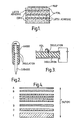
- One form of light emission device constructed on the "jack-plug" principle is shown in Figure 2 and Figure 3 indicates, schematically, a display device connected to a power source.
- the power source may be battery or mains.
- the display device comprises a plurality of confronting layers of electrical insulation disposed between confronting layers of electrically conductive material.
- the display device has a base support layer E, made of for example plywood and above this, a further insulation material e.g. a cork layer D, which may alternatively be made of a knitted material.
- the insulation in the device may comprise one or more different materials as may the conductive layers. material.
- a pair of electrically conductive layers B is located above the cork layer D, which may be made of "knitmesh", i.e. stainless steel and/or copper, copper alloy or other suitable alloy, in the form of "socks” i.e. flattened tubes.
- Woven or non-woven metal-coated insulative fibres, e.g. glass fibres coated with Aluminium, may be alternatively employed as the electrically conductive material.
- insulation layers C between the conductive layers B can take the form of polypropylene "socks",
- This display board of typical thickness k" (1.24 cm.), is used by placing the layer to be displayed A, e.g. a map, over the outer knitmesh layer B and one or more light emission devices, e.g. as illustrated in Figure 2, may be inserted into the device so as to provide an electrical circuit between the conductive layers B and including the device. Power is supplied to the conductive layers and the light-emission device lights up. It should be understood that the light-emission device need not take the exact form shown in Figure 2.
- the conductive region may be of any desired size and shape so as to be able to electrically link the conductive layers in the display device and to cause light to be emitted from the filament. More than two conductive layers may be employed if desired in the display board.
- the display device of this invention is particularly effective for illuminating written or printed matter such as diagrams, maps and pictures. It may be employed in, for example,:-
- one or more insulation layers and/or more than two electrically conductive layers may be used. If the display device has more than-two confronting electrically conductive layers, light emission devices of different lengths are employed so as to be able to electrically connect a different one of the pairs of electrically conductive layers. Thus, different light emission devices and areas of the item to be displayed may be lit up independently of one another, at the same or different times.
- the display device according to this invention may occupy only a part of a larger display device.
Landscapes
- Engineering & Computer Science (AREA)
- Ceramic Engineering (AREA)
- Physics & Mathematics (AREA)
- General Physics & Mathematics (AREA)
- Theoretical Computer Science (AREA)
- Illuminated Signs And Luminous Advertising (AREA)
Applications Claiming Priority (2)
| Application Number | Priority Date | Filing Date | Title |
|---|---|---|---|
| GB8233310 | 1982-11-23 | ||
| GB8233310 | 1982-11-23 |
Publications (2)
| Publication Number | Publication Date |
|---|---|
| EP0109852A2 true EP0109852A2 (fr) | 1984-05-30 |
| EP0109852A3 EP0109852A3 (fr) | 1984-12-05 |
Family
ID=10534426
Family Applications (1)
| Application Number | Title | Priority Date | Filing Date |
|---|---|---|---|
| EP83307108A Withdrawn EP0109852A3 (fr) | 1982-11-23 | 1983-11-21 | Dispositif d'affichage |
Country Status (1)
| Country | Link |
|---|---|
| EP (1) | EP0109852A3 (fr) |
Cited By (6)
| Publication number | Priority date | Publication date | Assignee | Title |
|---|---|---|---|---|
| GB2201023A (en) * | 1987-02-10 | 1988-08-17 | Oxley Dev Co Ltd | Information display systems |
| EP0305525A4 (en) * | 1987-01-12 | 1991-07-31 | Sekisui Kagaku Kogyo Kabushiki Kaisha | Electrically conductive transparent material and a display device using the electrically conductive material |
| US5218351A (en) * | 1987-01-12 | 1993-06-08 | Sekisui Kagaku Kogyo Kabushiki Kaisha | Electrically conductive transparent material and display device using the electrically conductive transparent material |
| WO2009101561A1 (fr) * | 2008-02-14 | 2009-08-20 | Koninklijke Philips Electronics N.V. | Système d'éclairage, source de lumière et dispositif d'électrode |
| EP3708360A1 (fr) * | 2019-03-11 | 2020-09-16 | Instituto Superior de Engenharia do Porto | Électrodes imprimées sur des substrats de liège et leur procédé d'obtention |
| WO2020244953A1 (fr) * | 2019-06-04 | 2020-12-10 | Berner Fachhochschule - Biel Architektur, Holz Und Bau | Élément structural présentant des propriétés électriquement conductrices et son procédé de fabrication |
Family Cites Families (3)
| Publication number | Priority date | Publication date | Assignee | Title |
|---|---|---|---|---|
| US3383641A (en) * | 1966-01-20 | 1968-05-14 | Goldberg Barry R | Electric supply means |
| FR2196101A5 (fr) * | 1972-08-08 | 1974-03-08 | Elfverson Goran | |
| DE2514995A1 (de) * | 1975-04-05 | 1976-10-14 | Helmut Gerd Scholl | Nadellampe mit kontakttraegerplatte |
-
1983
- 1983-11-21 EP EP83307108A patent/EP0109852A3/fr not_active Withdrawn
Cited By (9)
| Publication number | Priority date | Publication date | Assignee | Title |
|---|---|---|---|---|
| EP0305525A4 (en) * | 1987-01-12 | 1991-07-31 | Sekisui Kagaku Kogyo Kabushiki Kaisha | Electrically conductive transparent material and a display device using the electrically conductive material |
| US5218351A (en) * | 1987-01-12 | 1993-06-08 | Sekisui Kagaku Kogyo Kabushiki Kaisha | Electrically conductive transparent material and display device using the electrically conductive transparent material |
| GB2201023A (en) * | 1987-02-10 | 1988-08-17 | Oxley Dev Co Ltd | Information display systems |
| GB2201023B (en) * | 1987-02-10 | 1990-12-19 | Oxley Dev Co Ltd | Improvements in information display systems |
| WO2009101561A1 (fr) * | 2008-02-14 | 2009-08-20 | Koninklijke Philips Electronics N.V. | Système d'éclairage, source de lumière et dispositif d'électrode |
| US8390184B2 (en) | 2008-02-14 | 2013-03-05 | Koninklijke Philips Electronics N.V. | Lighting system, light source and electrode device |
| CN101946122B (zh) * | 2008-02-14 | 2014-12-31 | 皇家飞利浦电子股份有限公司 | 照明系统、光源和电极设备 |
| EP3708360A1 (fr) * | 2019-03-11 | 2020-09-16 | Instituto Superior de Engenharia do Porto | Électrodes imprimées sur des substrats de liège et leur procédé d'obtention |
| WO2020244953A1 (fr) * | 2019-06-04 | 2020-12-10 | Berner Fachhochschule - Biel Architektur, Holz Und Bau | Élément structural présentant des propriétés électriquement conductrices et son procédé de fabrication |
Also Published As
| Publication number | Publication date |
|---|---|
| EP0109852A3 (fr) | 1984-12-05 |
Similar Documents
| Publication | Publication Date | Title |
|---|---|---|
| US5621991A (en) | Lighted display with electroluminescent lamps | |
| JP4379762B2 (ja) | 照明、表示又は指示目的のための照明構成セット及びこのような照明構成セットのためのプラグコネクタ | |
| US4920467A (en) | Controlled stratified random area illuminator | |
| US3383641A (en) | Electric supply means | |
| US4752756A (en) | Electrical system with at least one electric load unit being disconnectably arranged on a surface | |
| TW375861B (en) | Wiring board constructions and methods of making same | |
| EP2043075A3 (fr) | Signe éclairé utilisant des diodes électroluminescentes | |
| EP0109852A2 (fr) | Dispositif d'affichage | |
| EP0305730A3 (en) | Holder for a small lamp bulb | |
| US4402151A (en) | Visual display arrangement | |
| US11193635B2 (en) | Flexible and cuttable LED sheet | |
| US3447253A (en) | Illuminated display sign | |
| SE9402546L (sv) | Elektroluminescerande anordning samt sätt att framställa denna | |
| US5672937A (en) | Light-transmitting electroconductive plastic film electrodes and method of manufacture | |
| BR9806993A (pt) | Dispositivo para a exibição de sinais alfa-numéricos e/ou sinais de imagem. | |
| US4783578A (en) | Multi-conductor cables | |
| JP2004071342A (ja) | 照明装置 | |
| JPH11305699A (ja) | 基板および該基板を用いた電光表示器 | |
| JP2000148050A (ja) | 表示装置とその部品 | |
| EP1045368A2 (fr) | Enseigne lumineuse | |
| US3815204A (en) | Apparatus and method for selectively backlighting printed circuit board perforations to accurately locate electrical component leads therein | |
| KR800000196Y1 (ko) | 전광 표시장치 | |
| JPH0434550Y2 (fr) | ||
| EP0933589A3 (fr) | Dispositif d' éclairage à espacement variable | |
| DE10112328A1 (de) | Elektrolumineszenz-Einrichtung |
Legal Events
| Date | Code | Title | Description |
|---|---|---|---|
| PUAI | Public reference made under article 153(3) epc to a published international application that has entered the european phase |
Free format text: ORIGINAL CODE: 0009012 |
|
| AK | Designated contracting states |
Designated state(s): AT BE CH DE FR GB IT LI LU NL SE |
|
| PUAL | Search report despatched |
Free format text: ORIGINAL CODE: 0009013 |
|
| RHK1 | Main classification (correction) |
Ipc: G09F 13/28 |
|
| AK | Designated contracting states |
Designated state(s): AT BE CH DE FR GB IT LI LU NL SE |
|
| 17P | Request for examination filed |
Effective date: 19850531 |
|
| 17Q | First examination report despatched |
Effective date: 19860613 |
|
| R17C | First examination report despatched (corrected) |
Effective date: 19870203 |
|
| STAA | Information on the status of an ep patent application or granted ep patent |
Free format text: STATUS: THE APPLICATION IS DEEMED TO BE WITHDRAWN |
|
| 18D | Application deemed to be withdrawn |
Effective date: 19880809 |
|
| RIN1 | Information on inventor provided before grant (corrected) |
Inventor name: ROUTH, HELEN Inventor name: MORGAN, PETER HUW Inventor name: WHEATLEY, BARRY IVAN Inventor name: SOMERFORD, DAVID JOHN |