EP0110257A2 - Circuit pour adresser des dispositifs - Google Patents
Circuit pour adresser des dispositifs Download PDFInfo
- Publication number
- EP0110257A2 EP0110257A2 EP83111516A EP83111516A EP0110257A2 EP 0110257 A2 EP0110257 A2 EP 0110257A2 EP 83111516 A EP83111516 A EP 83111516A EP 83111516 A EP83111516 A EP 83111516A EP 0110257 A2 EP0110257 A2 EP 0110257A2
- Authority
- EP
- European Patent Office
- Prior art keywords
- signal
- receiver
- receivers
- address
- address signal
- Prior art date
- Legal status (The legal status is an assumption and is not a legal conclusion. Google has not performed a legal analysis and makes no representation as to the accuracy of the status listed.)
- Granted
Links
Images
Classifications
-
- G—PHYSICS
- G01—MEASURING; TESTING
- G01R—MEASURING ELECTRIC VARIABLES; MEASURING MAGNETIC VARIABLES
- G01R31/00—Arrangements for testing electric properties; Arrangements for locating electric faults; Arrangements for electrical testing characterised by what is being tested not provided for elsewhere
- G01R31/50—Testing of electric apparatus, lines, cables or components for short-circuits, continuity, leakage current or incorrect line connections
- G01R31/66—Testing of connections, e.g. of plugs or non-disconnectable joints
- G01R31/67—Testing the correctness of wire connections in electric apparatus or circuits
Definitions
- the invention relates to a circuit arrangement for addressing modules with address receivers arranged on the individual modules.
- US Pat. No. 3,784,910 describes a wiring test system which can be selected in subordinate levels. Such test systems serve, for example, the proper wiring of a variety of wiring - support points determine. Some of these multitude of support points are connected by networks to form networks. The faultless connection of the wiring bases of these networks and their mutual isolation must be checked for each wiring base. For this purpose, the wiring support points, which simultaneously form the test points of a test object, must be individually selectable. It is often a number of checkpoints on the order of 100,000 or more. would have such a number will be immediately selected check points, thus help of parallel addressing many lines would be required, the test points associated für Anlagenschalt Vietnamese addressing many lines would be required, the test points associated Ardigeschalt Vietnamesee of the test - systems had to the interface of a computer to connect.
- control of the individual assemblies by means of a shift register acts like a selection by means of a rotary switch. No module can be selected without the previous modules having been selected beforehand. The speed is also dependent on the clock pulse frequency.
- the invention was intended to provide a circuit arrangement for addressing assemblies with which individual assemblies can be selected selectively without the need for a decoder which is complex for a large number of assemblies.
- the receiver consists of additive logic elements with two inputs for a coded address signal on the one hand and a digital change signal which is the same for all receivers on the other hand and two outputs for that according to the combination and the Change signal changed address signal on the one hand and for a decoded signal corresponding to a predetermined value of the changed address signal in the receiver on the other hand and the address signal outputs from previous receivers are connected to the address signal inputs of subsequent receivers.
- the additive logic elements consist of subtractors.
- the address receiver assigned to the first module receives an encoded address signal which consists of the ordinal number of the receiver to be selected.
- the change signal that is the same for each receiver consists of the least significant bit set.
- the value zero of the changed address signal, which occurs as a result of the subtraction in the subtractor of the selected receiver, serves as the decoded signal.
- the coded address signal input into the first receiver must consist of less than one of the ordinal number of the receiver to be selected.
- adders are used as additive logic gates in the address receivers.
- the coded address signal given to the first receiver in this exemplary embodiment consists of the number complementary to the ordinal number of the receiver to be selected with regard to the number of receivers.
- the change signal consists of the least significant bit set, and the decoded signal becomes a value corresponding to the number of receivers of the changed address signal. It is assumed that the bit width of the adder is equal to the number of receivers that can be selected.
- the coded address signal given to the first receiver consists of the number which is complementary to the ordinal number of the receiver to be selected with respect to the number of receivers, but which is increased by one.
- a third exemplary embodiment of a circuit arrangement for addressing modules with address receivers arranged on the individual modules has receivers which each comprise a comparator and a subtractor.
- a coded address signal is connected in parallel to one of two inputs of each comparator.
- the other input of each comparator is connected to the output of the subtractor assigned to it, to the minus end input of which the output of the subtractor of a previous receiver is connected.
- the least significant bit is set at the subtrahend inputs of all subtractors. The highest address plus one is always placed at the end of the minute of the first of the subtractors connected in series. If the signals compared in the comparator match, the latter emits a decoded signal.
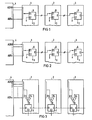
- three assemblies 1, 2 and 3 of a wiring tester can be selected via an interface 4 of a microprocessor which belongs to the wiring tester.
- the second assembly is representative of several assemblies that lie between the first assembly 1 and the last assembly 3.
- Modules 1 ... 3 can be selected via address receivers that are arranged on the modules.
- the address receivers consist of additive logic elements B, each with two inputs E1 and E2 and two outputs E and D.
- the outputs E of previous address receivers are connected with n bit lines to the inputs E1 of subsequent address receivers.
- the input E1 of the first address receiver is connected to the bit outputs of the interface 4.
- the additive logic elements B from which the address receivers are made, are subtractors in the exemplary embodiment according to FIG.
- the inputs E1 are the minuend inputs and the inputs E2 the subtrahend inputs.
- the least significant bit is set at inputs E2.
- a predetermined value of the address signal changed in the receiver is present at output D as a decoded signal.
- the fifth module is addressed with an 8-bit address signal, the address is in binary notation:
- the signals are for the fifth module
- the addressed module matches the decoded module.
- the original address signal must be reduced by one in order to reach the module to be selected.
- the exemplary embodiment according to FIG. 2 largely corresponds externally to the exemplary embodiment according to FIG. 1, but the additive logic element A assigned to the individual modules as the address receiver is an adder in the exemplary embodiment according to FIG.
- the coded address signal supplied to the input E1 of the first address receiver is the number complementary to the ordinal number of the receiver to be selected with respect to the number of receivers.
- the least significant bit is set again at input E2.
- the output E of a previous receiver is connected to the input E1 of a subsequent receiver.
- a decoded signal can be taken off at the output D which corresponds to a value of the changed address signal corresponding to the number of receivers.
- the decimal values of the binary signals are given in brackets.
- the second assembly is
- the corresponding signals for the fifth module are:
- signals are given for the address receivers of the first to sixth modules (the third and fourth modules have been omitted for the sake of simplicity) which are present at a third output carry and not at the address receivers of FIG. 2 and at output E.
- the shorter notation was used for output E because of the decadic numbers.
- the coded address signal to be fed into the address receiver of the first module must be increased by one so that the module to be selected is reached.
- three assemblies 1, 2 and 3 of a wiring tester can be selected via an interface 4 of a microprocessor that belongs to the wiring tester.
- the addresses for the modules each have n bits, the number n depends on the number of modules.
- Modules 1 ... 3 can be selected via address receivers that are arranged on the modules.
- the address receivers in this embodiment of the invention each consist of a comparator V and an additive logic element F.
- the logic element F is a subtractor.
- Bit outputs of the interface 4 for the address signal are located in parallel at inputs E3 of the comparator V.
- the output E of the additive logic elements F is connected to a second input E4 of the assigned comparator.
- the outputs E of preceding additive logic elements are connected to the inputs E1 of subsequent logic elements.
- the least significant bit is set at inputs E2, the subtrahend inputs of the additive logic elements F.
- a signal which corresponds to the largest possible address plus one is applied to the input E1 of the additive logic element assigned to the module 1.
- the result of the subtraction in each additive logic element F is compared with the address signal at the input E3 of the corresponding comparator V. If the signals match, the comparator V outputs a decoded signal at its output D.
Landscapes
- Physics & Mathematics (AREA)
- General Physics & Mathematics (AREA)
- Logic Circuits (AREA)
- Ultra Sonic Daignosis Equipment (AREA)
- Tests Of Electronic Circuits (AREA)
Priority Applications (1)
| Application Number | Priority Date | Filing Date | Title |
|---|---|---|---|
| AT83111516T ATE32632T1 (de) | 1982-11-29 | 1983-11-17 | Schaltungsanordnung zur adressierung von baugruppen. |
Applications Claiming Priority (2)
| Application Number | Priority Date | Filing Date | Title |
|---|---|---|---|
| DE19823244081 DE3244081A1 (de) | 1982-11-29 | 1982-11-29 | Schaltungsanordnung zur adressierung von baugruppen |
| DE3244081 | 1982-11-29 |
Publications (3)
| Publication Number | Publication Date |
|---|---|
| EP0110257A2 true EP0110257A2 (fr) | 1984-06-13 |
| EP0110257A3 EP0110257A3 (en) | 1985-06-19 |
| EP0110257B1 EP0110257B1 (fr) | 1988-02-24 |
Family
ID=6179317
Family Applications (1)
| Application Number | Title | Priority Date | Filing Date |
|---|---|---|---|
| EP83111516A Expired EP0110257B1 (fr) | 1982-11-29 | 1983-11-17 | Circuit pour adresser des dispositifs |
Country Status (3)
| Country | Link |
|---|---|
| EP (1) | EP0110257B1 (fr) |
| AT (1) | ATE32632T1 (fr) |
| DE (2) | DE3244081A1 (fr) |
Families Citing this family (2)
| Publication number | Priority date | Publication date | Assignee | Title |
|---|---|---|---|---|
| DE3542162A1 (de) * | 1984-09-11 | 1987-05-27 | Atp Arbeit Tech Photosynthese | Mikroelektronisches messdaten-erfassungssystem |
| GB2180972A (en) * | 1985-09-27 | 1987-04-08 | Philips Electronic Associated | Generating addresses for circuit units |
Family Cites Families (7)
| Publication number | Priority date | Publication date | Assignee | Title |
|---|---|---|---|---|
| DE2119387C3 (de) * | 1971-04-21 | 1979-12-20 | Siemens Ag, 1000 Berlin Und 8000 Muenchen | Schaltungsanordnung zur adressenabhängigen Ausgabe von Meldungen in Einrichtungen der Fernwirktechnik |
| US3784910A (en) * | 1972-07-13 | 1974-01-08 | Teradyne Inc | Sequential addressing network testing system |
| US3795860A (en) * | 1972-07-13 | 1974-03-05 | Teradyne Inc | Network tester employing latched test switching units |
| DE3039067A1 (de) * | 1980-10-16 | 1982-04-29 | Licentia Patent-Verwaltungs-Gmbh, 6000 Frankfurt | Verfahren zur pruefung von gedruckten schaltungsplatinen |
| DE3041811C2 (de) * | 1980-11-06 | 1984-04-05 | ANT Nachrichtentechnik GmbH, 7150 Backnang | Fernwirksystem mit zyklischer Weiterzählung |
| DE3110614C2 (de) * | 1981-03-18 | 1986-05-15 | Siemens AG, 1000 Berlin und 8000 München | Fernwirkeinrichtung mit mehreren Bereichsnetzen |
| DE3116079A1 (de) * | 1981-04-23 | 1982-11-11 | Robert Bosch Gmbh, 7000 Stuttgart | Pruefsystem |
-
1982
- 1982-11-29 DE DE19823244081 patent/DE3244081A1/de not_active Withdrawn
-
1983
- 1983-11-17 AT AT83111516T patent/ATE32632T1/de not_active IP Right Cessation
- 1983-11-17 EP EP83111516A patent/EP0110257B1/fr not_active Expired
- 1983-11-17 DE DE8383111516T patent/DE3375741D1/de not_active Expired
Also Published As
| Publication number | Publication date |
|---|---|
| EP0110257A3 (en) | 1985-06-19 |
| ATE32632T1 (de) | 1988-03-15 |
| DE3244081A1 (de) | 1984-05-30 |
| DE3375741D1 (en) | 1988-03-31 |
| EP0110257B1 (fr) | 1988-02-24 |
Similar Documents
| Publication | Publication Date | Title |
|---|---|---|
| DE2256135C3 (de) | Verfahren zum Prüfen von monolithisch integrierten Halbleiterschaltungen | |
| DE3215671C2 (de) | Programmierbare Logikanordnung | |
| DE2457312A1 (de) | Datenbehandlungseinrichtung mit einem feldwaehler | |
| DE2007353C3 (de) | Vierteiliges Addierwerk | |
| DE3120669C2 (de) | A/D - und D/A - Umsetzer | |
| DE2224389A1 (de) | Speichersystem | |
| DE2247704A1 (de) | Aus monolithisch integrierten schaltkreisen aufgebaute datenverarbeitungsanlage | |
| DE3525395C2 (fr) | ||
| DE2361512C2 (de) | Schaltungsanordnung zur Prüfung eines Additionsresultates | |
| DE1937249A1 (de) | Selbstpruefende Fehlererkennungsschaltung | |
| DE2433075A1 (de) | Anordnung zur frequenzsynthese | |
| DE3526521C2 (fr) | ||
| EP0130397A1 (fr) | Appareil de calcul numérique | |
| EP0048352A1 (fr) | Additionneur binaire parallèle en technique MOS à retenues transmises par commutation | |
| EP0110257B1 (fr) | Circuit pour adresser des dispositifs | |
| DE1234054B (de) | Byte-Umsetzer | |
| DE1806172A1 (de) | Prioritaetsschaltung | |
| DE69026363T2 (de) | Multipositionsverschieber mit Paritätsbitgenerator | |
| DE2004934B2 (de) | Speicheranordnung mit schaltungen zur fehlererkennung und fehlerkorrektur | |
| DE3587401T2 (de) | Maskensignalgenerator. | |
| DE3640670C2 (fr) | ||
| EP0840230A2 (fr) | Dispositif de sélection de mots d'adresse utilisant du décodage de démultiplexage | |
| EP0065037B1 (fr) | Montage pour un dispositif de liaison logique constitué de modules semi-conducteurs analogues | |
| DE1574603A1 (de) | Binaere Addierschaltung | |
| DE1412097C (de) | Elektronisches Schrittschaltwerk in Form einer Ringschaltung |
Legal Events
| Date | Code | Title | Description |
|---|---|---|---|
| PUAI | Public reference made under article 153(3) epc to a published international application that has entered the european phase |
Free format text: ORIGINAL CODE: 0009012 |
|
| AK | Designated contracting states |
Designated state(s): AT CH DE FR IT LI NL SE |
|
| 17P | Request for examination filed |
Effective date: 19841220 |
|
| PUAL | Search report despatched |
Free format text: ORIGINAL CODE: 0009013 |
|
| RHK1 | Main classification (correction) |
Ipc: G01R 31/28 |
|
| AK | Designated contracting states |
Designated state(s): AT CH DE FR IT LI NL SE |
|
| 17Q | First examination report despatched |
Effective date: 19860908 |
|
| GRAA | (expected) grant |
Free format text: ORIGINAL CODE: 0009210 |
|
| AK | Designated contracting states |
Kind code of ref document: B1 Designated state(s): AT CH DE FR IT LI NL SE |
|
| REF | Corresponds to: |
Ref document number: 32632 Country of ref document: AT Date of ref document: 19880315 Kind code of ref document: T |
|
| PG25 | Lapsed in a contracting state [announced via postgrant information from national office to epo] |
Ref country code: SE Effective date: 19880229 |
|
| REF | Corresponds to: |
Ref document number: 3375741 Country of ref document: DE Date of ref document: 19880331 |
|
| ET | Fr: translation filed | ||
| ITF | It: translation for a ep patent filed | ||
| PLBE | No opposition filed within time limit |
Free format text: ORIGINAL CODE: 0009261 |
|
| STAA | Information on the status of an ep patent application or granted ep patent |
Free format text: STATUS: NO OPPOSITION FILED WITHIN TIME LIMIT |
|
| 26N | No opposition filed | ||
| PGFP | Annual fee paid to national office [announced via postgrant information from national office to epo] |
Ref country code: AT Payment date: 19911030 Year of fee payment: 9 |
|
| PGFP | Annual fee paid to national office [announced via postgrant information from national office to epo] |
Ref country code: FR Payment date: 19911122 Year of fee payment: 9 |
|
| ITTA | It: last paid annual fee | ||
| PGFP | Annual fee paid to national office [announced via postgrant information from national office to epo] |
Ref country code: NL Payment date: 19911130 Year of fee payment: 9 |
|
| PGFP | Annual fee paid to national office [announced via postgrant information from national office to epo] |
Ref country code: DE Payment date: 19920128 Year of fee payment: 9 |
|
| PGFP | Annual fee paid to national office [announced via postgrant information from national office to epo] |
Ref country code: CH Payment date: 19920221 Year of fee payment: 9 |
|
| PG25 | Lapsed in a contracting state [announced via postgrant information from national office to epo] |
Ref country code: AT Effective date: 19921117 |
|
| PG25 | Lapsed in a contracting state [announced via postgrant information from national office to epo] |
Ref country code: LI Effective date: 19921130 Ref country code: CH Effective date: 19921130 |
|
| PG25 | Lapsed in a contracting state [announced via postgrant information from national office to epo] |
Ref country code: NL Effective date: 19930601 |
|
| NLV4 | Nl: lapsed or anulled due to non-payment of the annual fee | ||
| PG25 | Lapsed in a contracting state [announced via postgrant information from national office to epo] |
Ref country code: FR Effective date: 19930730 |
|
| REG | Reference to a national code |
Ref country code: CH Ref legal event code: PL |
|
| REG | Reference to a national code |
Ref country code: FR Ref legal event code: ST |
|
| PG25 | Lapsed in a contracting state [announced via postgrant information from national office to epo] |
Ref country code: DE Effective date: 19940101 |