EP0110468A1 - Méthode pour faire croître un film d'alliage sur un substrat par un procédé couche par couche, et méthode de fabrication d'un dispositif semi-conducteur - Google Patents
Méthode pour faire croître un film d'alliage sur un substrat par un procédé couche par couche, et méthode de fabrication d'un dispositif semi-conducteur Download PDFInfo
- Publication number
- EP0110468A1 EP0110468A1 EP83201640A EP83201640A EP0110468A1 EP 0110468 A1 EP0110468 A1 EP 0110468A1 EP 83201640 A EP83201640 A EP 83201640A EP 83201640 A EP83201640 A EP 83201640A EP 0110468 A1 EP0110468 A1 EP 0110468A1
- Authority
- EP
- European Patent Office
- Prior art keywords
- alloy
- film
- growth
- growth rate
- growing
- Prior art date
- Legal status (The legal status is an assumption and is not a legal conclusion. Google has not performed a legal analysis and makes no representation as to the accuracy of the status listed.)
- Granted
Links
- 229910045601 alloy Inorganic materials 0.000 title claims abstract description 131
- 239000000956 alloy Substances 0.000 title claims abstract description 131
- 239000000758 substrate Substances 0.000 title claims abstract description 62
- 238000000034 method Methods 0.000 title claims abstract description 57
- 238000004519 manufacturing process Methods 0.000 title claims abstract description 6
- 239000004065 semiconductor Substances 0.000 title claims abstract description 6
- 239000010410 layer Substances 0.000 claims abstract description 58
- 230000010355 oscillation Effects 0.000 claims abstract description 32
- 239000000470 constituent Substances 0.000 claims abstract description 29
- 239000002356 single layer Substances 0.000 claims abstract description 9
- PCTMTFRHKVHKIS-BMFZQQSSSA-N (1s,3r,4e,6e,8e,10e,12e,14e,16e,18s,19r,20r,21s,25r,27r,30r,31r,33s,35r,37s,38r)-3-[(2r,3s,4s,5s,6r)-4-amino-3,5-dihydroxy-6-methyloxan-2-yl]oxy-19,25,27,30,31,33,35,37-octahydroxy-18,20,21-trimethyl-23-oxo-22,39-dioxabicyclo[33.3.1]nonatriaconta-4,6,8,10 Chemical compound C1C=C2C[C@@H](OS(O)(=O)=O)CC[C@]2(C)[C@@H]2[C@@H]1[C@@H]1CC[C@H]([C@H](C)CCCC(C)C)[C@@]1(C)CC2.O[C@H]1[C@@H](N)[C@H](O)[C@@H](C)O[C@H]1O[C@H]1/C=C/C=C/C=C/C=C/C=C/C=C/C=C/[C@H](C)[C@@H](O)[C@@H](C)[C@H](C)OC(=O)C[C@H](O)C[C@H](O)CC[C@@H](O)[C@H](O)C[C@H](O)C[C@](O)(C[C@H](O)[C@H]2C(O)=O)O[C@H]2C1 PCTMTFRHKVHKIS-BMFZQQSSSA-N 0.000 claims description 30
- 150000001875 compounds Chemical class 0.000 claims description 24
- 239000000203 mixture Substances 0.000 claims description 11
- 238000001451 molecular beam epitaxy Methods 0.000 claims description 9
- 229910000756 V alloy Inorganic materials 0.000 claims description 8
- 230000001678 irradiating effect Effects 0.000 claims description 8
- 230000000737 periodic effect Effects 0.000 claims description 5
- 238000007738 vacuum evaporation Methods 0.000 claims description 4
- 229910002056 binary alloy Inorganic materials 0.000 claims description 3
- 238000000151 deposition Methods 0.000 claims description 3
- 229910002059 quaternary alloy Inorganic materials 0.000 claims 1
- 241000894007 species Species 0.000 description 27
- JBRZTFJDHDCESZ-UHFFFAOYSA-N AsGa Chemical compound [As]#[Ga] JBRZTFJDHDCESZ-UHFFFAOYSA-N 0.000 description 20
- 229910001218 Gallium arsenide Inorganic materials 0.000 description 20
- 229910052782 aluminium Inorganic materials 0.000 description 14
- 230000004907 flux Effects 0.000 description 10
- GYHNNYVSQQEPJS-UHFFFAOYSA-N Gallium Chemical compound [Ga] GYHNNYVSQQEPJS-UHFFFAOYSA-N 0.000 description 6
- 229910052733 gallium Inorganic materials 0.000 description 6
- 239000004411 aluminium Substances 0.000 description 5
- XAGFODPZIPBFFR-UHFFFAOYSA-N aluminium Chemical compound [Al] XAGFODPZIPBFFR-UHFFFAOYSA-N 0.000 description 5
- 238000002003 electron diffraction Methods 0.000 description 3
- 150000002500 ions Chemical class 0.000 description 3
- 238000002128 reflection high energy electron diffraction Methods 0.000 description 3
- 229910052710 silicon Inorganic materials 0.000 description 3
- IJGRMHOSHXDMSA-UHFFFAOYSA-N Atomic nitrogen Chemical compound N#N IJGRMHOSHXDMSA-UHFFFAOYSA-N 0.000 description 2
- XUIMIQQOPSSXEZ-UHFFFAOYSA-N Silicon Chemical compound [Si] XUIMIQQOPSSXEZ-UHFFFAOYSA-N 0.000 description 2
- 229910000577 Silicon-germanium Inorganic materials 0.000 description 2
- FAPWRFPIFSIZLT-UHFFFAOYSA-M Sodium chloride Chemical compound [Na+].[Cl-] FAPWRFPIFSIZLT-UHFFFAOYSA-M 0.000 description 2
- LEVVHYCKPQWKOP-UHFFFAOYSA-N [Si].[Ge] Chemical compound [Si].[Ge] LEVVHYCKPQWKOP-UHFFFAOYSA-N 0.000 description 2
- MDPILPRLPQYEEN-UHFFFAOYSA-N aluminium arsenide Chemical compound [As]#[Al] MDPILPRLPQYEEN-UHFFFAOYSA-N 0.000 description 2
- 229910052785 arsenic Inorganic materials 0.000 description 2
- RQNWIZPPADIBDY-UHFFFAOYSA-N arsenic atom Chemical compound [As] RQNWIZPPADIBDY-UHFFFAOYSA-N 0.000 description 2
- 229910052732 germanium Inorganic materials 0.000 description 2
- 229910021478 group 5 element Inorganic materials 0.000 description 2
- 229910021476 group 6 element Inorganic materials 0.000 description 2
- LQBJWKCYZGMFEV-UHFFFAOYSA-N lead tin Chemical compound [Sn].[Pb] LQBJWKCYZGMFEV-UHFFFAOYSA-N 0.000 description 2
- 239000010703 silicon Substances 0.000 description 2
- 229910052718 tin Inorganic materials 0.000 description 2
- 239000002023 wood Substances 0.000 description 2
- YBNMDCCMCLUHBL-UHFFFAOYSA-N (2,5-dioxopyrrolidin-1-yl) 4-pyren-1-ylbutanoate Chemical compound C=1C=C(C2=C34)C=CC3=CC=CC4=CC=C2C=1CCCC(=O)ON1C(=O)CCC1=O YBNMDCCMCLUHBL-UHFFFAOYSA-N 0.000 description 1
- MARUHZGHZWCEQU-UHFFFAOYSA-N 5-phenyl-2h-tetrazole Chemical compound C1=CC=CC=C1C1=NNN=N1 MARUHZGHZWCEQU-UHFFFAOYSA-N 0.000 description 1
- 229910002696 Ag-Au Inorganic materials 0.000 description 1
- 240000001492 Carallia brachiata Species 0.000 description 1
- 229910000661 Mercury cadmium telluride Inorganic materials 0.000 description 1
- BQCADISMDOOEFD-UHFFFAOYSA-N Silver Chemical compound [Ag] BQCADISMDOOEFD-UHFFFAOYSA-N 0.000 description 1
- ATJFFYVFTNAWJD-UHFFFAOYSA-N Tin Chemical compound [Sn] ATJFFYVFTNAWJD-UHFFFAOYSA-N 0.000 description 1
- MCMSPRNYOJJPIZ-UHFFFAOYSA-N cadmium;mercury;tellurium Chemical compound [Cd]=[Te]=[Hg] MCMSPRNYOJJPIZ-UHFFFAOYSA-N 0.000 description 1
- 238000004140 cleaning Methods 0.000 description 1
- 239000013078 crystal Substances 0.000 description 1
- 230000003247 decreasing effect Effects 0.000 description 1
- 230000008021 deposition Effects 0.000 description 1
- 239000002019 doping agent Substances 0.000 description 1
- 230000000694 effects Effects 0.000 description 1
- 229910052949 galena Inorganic materials 0.000 description 1
- GNPVGFCGXDBREM-UHFFFAOYSA-N germanium atom Chemical compound [Ge] GNPVGFCGXDBREM-UHFFFAOYSA-N 0.000 description 1
- 229910021480 group 4 element Inorganic materials 0.000 description 1
- 238000002347 injection Methods 0.000 description 1
- 239000007924 injection Substances 0.000 description 1
- 238000011835 investigation Methods 0.000 description 1
- 239000007788 liquid Substances 0.000 description 1
- 229910001092 metal group alloy Inorganic materials 0.000 description 1
- 239000010445 mica Substances 0.000 description 1
- 229910052618 mica group Inorganic materials 0.000 description 1
- 229910052757 nitrogen Inorganic materials 0.000 description 1
- 239000010453 quartz Substances 0.000 description 1
- VYPSYNLAJGMNEJ-UHFFFAOYSA-N silicon dioxide Inorganic materials O=[Si]=O VYPSYNLAJGMNEJ-UHFFFAOYSA-N 0.000 description 1
- 229910052709 silver Inorganic materials 0.000 description 1
- 239000004332 silver Substances 0.000 description 1
- 239000011780 sodium chloride Substances 0.000 description 1
- 230000003068 static effect Effects 0.000 description 1
- OCGWQDWYSQAFTO-UHFFFAOYSA-N tellanylidenelead Chemical compound [Pb]=[Te] OCGWQDWYSQAFTO-UHFFFAOYSA-N 0.000 description 1
- XSOKHXFFCGXDJZ-UHFFFAOYSA-N telluride(2-) Chemical compound [Te-2] XSOKHXFFCGXDJZ-UHFFFAOYSA-N 0.000 description 1
- 229910002058 ternary alloy Inorganic materials 0.000 description 1
- 230000036962 time dependent Effects 0.000 description 1
Images
Classifications
-
- C—CHEMISTRY; METALLURGY
- C30—CRYSTAL GROWTH
- C30B—SINGLE-CRYSTAL GROWTH; UNIDIRECTIONAL SOLIDIFICATION OF EUTECTIC MATERIAL OR UNIDIRECTIONAL DEMIXING OF EUTECTOID MATERIAL; REFINING BY ZONE-MELTING OF MATERIAL; PRODUCTION OF A HOMOGENEOUS POLYCRYSTALLINE MATERIAL WITH DEFINED STRUCTURE; SINGLE CRYSTALS OR HOMOGENEOUS POLYCRYSTALLINE MATERIAL WITH DEFINED STRUCTURE; AFTER-TREATMENT OF SINGLE CRYSTALS OR A HOMOGENEOUS POLYCRYSTALLINE MATERIAL WITH DEFINED STRUCTURE; APPARATUS THEREFOR
- C30B23/00—Single-crystal growth by condensing evaporated or sublimed materials
- C30B23/02—Epitaxial-layer growth
-
- C—CHEMISTRY; METALLURGY
- C23—COATING METALLIC MATERIAL; COATING MATERIAL WITH METALLIC MATERIAL; CHEMICAL SURFACE TREATMENT; DIFFUSION TREATMENT OF METALLIC MATERIAL; COATING BY VACUUM EVAPORATION, BY SPUTTERING, BY ION IMPLANTATION OR BY CHEMICAL VAPOUR DEPOSITION, IN GENERAL; INHIBITING CORROSION OF METALLIC MATERIAL OR INCRUSTATION IN GENERAL
- C23C—COATING METALLIC MATERIAL; COATING MATERIAL WITH METALLIC MATERIAL; SURFACE TREATMENT OF METALLIC MATERIAL BY DIFFUSION INTO THE SURFACE, BY CHEMICAL CONVERSION OR SUBSTITUTION; COATING BY VACUUM EVAPORATION, BY SPUTTERING, BY ION IMPLANTATION OR BY CHEMICAL VAPOUR DEPOSITION, IN GENERAL
- C23C14/00—Coating by vacuum evaporation, by sputtering or by ion implantation of the coating forming material
- C23C14/22—Coating by vacuum evaporation, by sputtering or by ion implantation of the coating forming material characterised by the process of coating
- C23C14/54—Controlling or regulating the coating process
- C23C14/542—Controlling the film thickness or evaporation rate
- C23C14/545—Controlling the film thickness or evaporation rate using measurement on deposited material
-
- C—CHEMISTRY; METALLURGY
- C23—COATING METALLIC MATERIAL; COATING MATERIAL WITH METALLIC MATERIAL; CHEMICAL SURFACE TREATMENT; DIFFUSION TREATMENT OF METALLIC MATERIAL; COATING BY VACUUM EVAPORATION, BY SPUTTERING, BY ION IMPLANTATION OR BY CHEMICAL VAPOUR DEPOSITION, IN GENERAL; INHIBITING CORROSION OF METALLIC MATERIAL OR INCRUSTATION IN GENERAL
- C23C—COATING METALLIC MATERIAL; COATING MATERIAL WITH METALLIC MATERIAL; SURFACE TREATMENT OF METALLIC MATERIAL BY DIFFUSION INTO THE SURFACE, BY CHEMICAL CONVERSION OR SUBSTITUTION; COATING BY VACUUM EVAPORATION, BY SPUTTERING, BY ION IMPLANTATION OR BY CHEMICAL VAPOUR DEPOSITION, IN GENERAL
- C23C14/00—Coating by vacuum evaporation, by sputtering or by ion implantation of the coating forming material
- C23C14/22—Coating by vacuum evaporation, by sputtering or by ion implantation of the coating forming material characterised by the process of coating
- C23C14/54—Controlling or regulating the coating process
- C23C14/548—Controlling the composition
-
- C—CHEMISTRY; METALLURGY
- C30—CRYSTAL GROWTH
- C30B—SINGLE-CRYSTAL GROWTH; UNIDIRECTIONAL SOLIDIFICATION OF EUTECTIC MATERIAL OR UNIDIRECTIONAL DEMIXING OF EUTECTOID MATERIAL; REFINING BY ZONE-MELTING OF MATERIAL; PRODUCTION OF A HOMOGENEOUS POLYCRYSTALLINE MATERIAL WITH DEFINED STRUCTURE; SINGLE CRYSTALS OR HOMOGENEOUS POLYCRYSTALLINE MATERIAL WITH DEFINED STRUCTURE; AFTER-TREATMENT OF SINGLE CRYSTALS OR A HOMOGENEOUS POLYCRYSTALLINE MATERIAL WITH DEFINED STRUCTURE; APPARATUS THEREFOR
- C30B29/00—Single crystals or homogeneous polycrystalline material with defined structure characterised by the material or by their shape
- C30B29/10—Inorganic compounds or compositions
- C30B29/40—AIIIBV compounds wherein A is B, Al, Ga, In or Tl and B is N, P, As, Sb or Bi
-
- C—CHEMISTRY; METALLURGY
- C30—CRYSTAL GROWTH
- C30B—SINGLE-CRYSTAL GROWTH; UNIDIRECTIONAL SOLIDIFICATION OF EUTECTIC MATERIAL OR UNIDIRECTIONAL DEMIXING OF EUTECTOID MATERIAL; REFINING BY ZONE-MELTING OF MATERIAL; PRODUCTION OF A HOMOGENEOUS POLYCRYSTALLINE MATERIAL WITH DEFINED STRUCTURE; SINGLE CRYSTALS OR HOMOGENEOUS POLYCRYSTALLINE MATERIAL WITH DEFINED STRUCTURE; AFTER-TREATMENT OF SINGLE CRYSTALS OR A HOMOGENEOUS POLYCRYSTALLINE MATERIAL WITH DEFINED STRUCTURE; APPARATUS THEREFOR
- C30B29/00—Single crystals or homogeneous polycrystalline material with defined structure characterised by the material or by their shape
- C30B29/10—Inorganic compounds or compositions
- C30B29/46—Sulfur-, selenium- or tellurium-containing compounds
- C30B29/48—AIIBVI compounds wherein A is Zn, Cd or Hg, and B is S, Se or Te
-
- C—CHEMISTRY; METALLURGY
- C30—CRYSTAL GROWTH
- C30B—SINGLE-CRYSTAL GROWTH; UNIDIRECTIONAL SOLIDIFICATION OF EUTECTIC MATERIAL OR UNIDIRECTIONAL DEMIXING OF EUTECTOID MATERIAL; REFINING BY ZONE-MELTING OF MATERIAL; PRODUCTION OF A HOMOGENEOUS POLYCRYSTALLINE MATERIAL WITH DEFINED STRUCTURE; SINGLE CRYSTALS OR HOMOGENEOUS POLYCRYSTALLINE MATERIAL WITH DEFINED STRUCTURE; AFTER-TREATMENT OF SINGLE CRYSTALS OR A HOMOGENEOUS POLYCRYSTALLINE MATERIAL WITH DEFINED STRUCTURE; APPARATUS THEREFOR
- C30B29/00—Single crystals or homogeneous polycrystalline material with defined structure characterised by the material or by their shape
- C30B29/10—Inorganic compounds or compositions
- C30B29/52—Alloys
Definitions
- the invention relates to a method of growing an alloy film by a layer-by-layer process on a substrate, and determining the growth rate of the film by irradiating the growing alloy film with a beam of electrons and measuring the period of oscillations in the intensity of the stream of electrons diffracted at the growth surface, or specularly reflected by the growth surface, or emitted from the growth surface, or of the current flowing to earth through the substrate, which period is equal to the growth time of one monolayer of the alloy on the substrate.
- the invention also relates to a method of making a semiconductor device, in which method an alloy film is grown on a substrate by a layer-by-layer process, and the growth rate of the film is determined by irradiating the growing alloy film with a beam, of electrons and measuring the period of oscillations in the intensity of the stream of electrons diffractedat the growth surface, or specularly reflected by the growth surface, or emitted from the growth surface, or of the current flowing to earth through the substrate, which period is equal to the growth time of one monolayer of the alloy on the substrate.
- Alloy films may be grown by layer-by-layer processes such as vacuum evaporation or molecular beam processes.
- Molecular beam epitaxy processes are widely used in the manufacture of semiconductor devices, for example, in the fabrication of laser structures, when it is necessary to deposit III-V alloy films of controlled composition. Hitherto it has not been possible to determine the composition of an alloy film as it is being grown.
- the fluxes of the alloy constituents which are incident on a substrate have been measured using an ion gauge, or a quartz crystal rate monitor.
- the compositions of the alloy films have been measured after the substrates bearing the films have been removed from the growth systems.
- An object of the invention is to provide a method of determining the composition of an alloy film during growth of the film by a layer-by-layer process.
- a method according to the invention of growing an alloy film by a layer-by-layer process on a substrate is characterized in that at least one intermediate film consisting of at least one constituent of the alloy is grown between the substrate and the alloy film, that the growth rate of the/each intermediate film is determined by irradiating the growing intermediate film with a beam of electrons and measuring the period of oscillations in the intensity of the stream of electrons diffracted at the growth surface, specularly reflected by the growth surface, or emitted from the growth surface, or of the current flowing to earth through the substrate, and that the atomic ratio of constituents present in the alloy is calculated from the growth rates of the alloy film and of the intermediate film(s).
- the layer-by-layer process may be, for example, a vacuum evaporation process or a molecular beam epitaxy process.
- the growth rate of a film of an alloy A x B I - x is determined by the sum of the growth rates of the constituents A and B, it follows that the composition of the alloy can be determined by measuring the growth rates of a buffer layer of the element A on a substrate and of the alloy AB film grown on this buffer layer, by measuring the periods of the above-mentioned oscillations to determine the respective growth rates R A and R AB .
- the atomic fraction x of the element A present in the film of the alloy is given by
- the atomic fraction (1-x) of the element B is given by
- Apparatus used for growing films by molecular beam processes commonly includes an electron gun and a reflection electron difraction screen in order to monitor the cleanness of the substrate surface and the structure of the growth surface. Such apparatus will not require any additional items such as ion gauges within the growth system in order to perform a method according to the invention.
- a method according to the invention comprises the steps of growing a buffer layer of A on the substrate and determining the growth rate of the buffer layer, growing a film of the alloy AB on the buffer layer by continuing to deposit A on the growth surface without changing the conditions of the source supplying A and additionally depositing constituent B of the alloy on the growth surface, determining the growth rate of the alloy AB film, and calculating the ratio of the growth rate of the buffer layer to the growth rate of the alloy film which ratio is equal to the atomic fraction of A present in the alloy AB.
- Such a binary alloy film may be, for example, a metal alloy film, such as an Ag-Au film grown by vacuum evaporation on a silver buffer layer on a (111) NaCl layer present on a mica support, or a silicon-germanium film grown on a silicon support.
- a silicon buffer layer may be used.
- a method according to the invention comprises the steps of growing a buffer layer of the compound AB on the substrate and determining the growth rate of the buffer layer, growing the film of the alloy ABC by continuing to supply the species A and B to the growth surface without changing the conditions of the sources supplying the species A and B and additionally supplying species C to the growth surface, determining the growth rate of the film of the alloy ABC, calculating the growth rate of the constituent BC of the alloy ABC by substracting the growth rate of the buffer layer AB from the growth rate of the alloy film ABC, and calculating the ratio of the growth rate of the compound AB to the growth rate of the constituent BC, which ratio is equal to the atomic ratio A:C in the alloy film ABC.
- the alloy ABC may be, for example, Ga l - x AsAl x , when 1) x ) 0.
- a useful set of oscillations in the intensity of a stream of electrons diffracted at or specularly reflected by or emitted from the growth surface or flowing to earth through the substrate is observable at the start of growth, or may be produced, for example, by momentarily interrupting and then restarting a species flow onto a growth surface when growing a buffer layer.
- the intensity of these oscillations falls quite rapidly, but resumes at a useful level after such an interruption and restart.
- a useful set of oscillations is obtained without it being necessary subsequently to interrupt and restart this further species flow.
- a method according to the invention comprises the steps of growing a buffer layer of a compound AB on the substrate and determining the growth rate of the buffer layer, growing a film of an alloy ABC on the buffer layer by continuing to supply species A and B to the growth surface without changing the conditions of the sources supplying the species A and B and additionally supplying species C to the growth surface, determining the growth rate of the film of the alloy ABC, growing a film of the alloy ABCD on the alloy film ABC by continuing to supply species A, B and C to the growth surface without changing the conditions of the sources A, B and C and additionally supplying species D to the growth surface, and determining the growth rate of the film of the alloy ABCD, calculating the growth rates of the compounds BC and BD by subtracting the growth rates of the buffer layer and of the film ABC from the growth rates of the films ABC and ABCD respectively, and calculating the ratios of the
- a method according to the invention of making a 'semiconductor device for example, an injection laser, is characterized in that at least one intermediate film of at least one constituent of the alloy is grown between the substrate and the alloy film, that the growth rate of the/each intermediate film is determined by irradiating the growing intermediate film with a beam of electrons and measuring the period of oscillations in the intensity of the stream of electrons diffracted at the growth surface specularly reflected by the growth surface, or emitted from the growth surface, or of the current flowing to earth through the substrate, and that the atomic ratio of constituents present in the alloy is calculated from the growth rates of the alloy film and of the intermediate film(s).
- a method according to the invention comprises the steps of growing a buffer layer of a compound AB on the substrate and determining the growth rate of the buffer layer, growing a film of the alloy ABCD on the buffer layer AB by continuing to supply the species A and B to the growth surface without changing the conditions of the sources of A and B and additionally supplying species C and D to the growth surface, determining the growth rate of the film ABCD, calculating the growth rate of a compound CD by subtracting the growth rate of the buffer layer AB from the growth rate of the film ABCD, and calculating the ratio of the growth rate of the compound AB to the growth rate of the compound CD, which ratio is equal to the atomic ratio A:C in the alloy film ABCD.
- a method according to the invention comprises the steps of growing a film of A on the substrate and determining the growth rate of the film A, growing a film of a compound AB on the film A by continuing to supply species A to the growth surface without changing the conditions of the source supplying the species A and additionally supplying species B to the growth surface, determining the growth rate of the film AB, growing a film of the alloy ABC on the film of the alloy AB by continuing to supply the species A and B to the growth surface without changing the conditions of the sources supplying the species A and B and additionally supplying species C to the growth surface, determining the growth rate of the film of the alloy ABC, calculating the growth rate of the constituent B and C by subtracting the growth rates of the films of A and AB from the growth rate of the films AB and ABC respectively, and calculating the ratios of the growth rates of the constituents A:B:C,
- the ternary alloy ABC may be, for example, cadmium mercury telluride grown on a cadmium telluride substrate, lead tin telluride on a lead telluride substrate, or gallium aluminium arsenide grown on a gallium arsenide buffer layer on a germanium or a gallium arsenide substrate.
- a method according to the invention comprises the steps of growing a film of A on the substrate and determining the growth rate of the film A, growing a film of a compound AB on the film A by continuing to supply species A to the growth surface without changing the conditions of the source supplying the species A and additionally supplying species B to the growth surface, determining the growth rate of the film AB, growing a film of an alloy ABC on the film AB by continuing to supply species A and B to the growth surface without changing the conditions of the sources supplying the species A and B and additionally supplying species C to the growth surface, determining the growth rate of the film of the alloy ABC, growing a film of the alloy ABCD on the alloy film ABC by continuing to supply species A, B and C to the growth surface without changing the conditions of the sources A, B and C and additionally supplying species D to the growth surface, and determining the growth rate of the film of the alloy ABC
- the composition of the alloy film may be controlled by feeding input signals derived from the oscillations in the intensity of the stream of electrons diffracted from, or specularly reflected at, or emitted from the growth surface, or flowing to earth through the substrate into the control means, which input signals are compared by the control means with a preset value corresponding to a desired alloy composition, and wherein the control means adjust the operation of sources of constituent elements of the alloy supplying these elements to the alloy film growth surface until the input signals correspond to the preset value.
- the thickness of each film of the structure may be controlled by feeding input signals derived from the oscillations in the intensity of the stream of electrons diffracted from, or specularly reflected at, or emitted from the growth surface, or flowing to earth through the substrate, into the control means, and the control means are programmed to open and close shutters in front of effusion cells in sequence corresponding to the thickness and composition of constituent films of the structure.
- Such a superlattice structure may consist, for example, of 100 units of a combination of four monolayers (each 2.831 thick) of GaAs and five monolayers of Ga 0.5 Al 0.5 As (each 2.83 1 thick), and might be used as part of a short wavelength laser structure.
- the control means may also be used to control the composition of the Gao. 5 Alo. 5 As films as described above.
- the growth is determined by a reflection electron diffraction technique, it is preferred to monitor the oscillations in the intensity of the specularly reflected beam, since the intensity variations of this beam are larger than the intensity variations of individual diffracted beams.
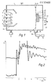
- a molecular beam epitaxy apparatus comprising a vacuum chamber 1 provided with effusion cells 3, 5, 7 and 9 each provided with a respective independently operable shutter 11, 13, 15 and 17, the cells and shutters being disposed within a shroud 19 cooled by liquid nitrogen.
- the apparatus includes an electron gun 21 used to irradiate a substrate 23 mounted on a rotatable substrate holder 25, in order to monitor the substrate cleaning and to determine the growth rate of a GaAs film 27 grown on the substrate 23 and to determine the growth rate of a (Ga,Al)As film 29 grown over the GaAs film 27.
- the growth rates were determined by measuring the period of oscillations in the intensity of a beam 31 of 12 keV electrons which was specularly reflected from the growth surface on to a reflection electron diffraction screen 35 and photons from the screen 35 were detected on a photodetector 33.
- the signals from the photodetector 33 were amplified by means of an amplifier 37 and were displayed as a trace on a display 39.
- the vacuum chamber 1 was exhausted by means of a pump system 41.
- the effusion cells 3, 5, 7 and 9 which were loaded with gallium, arsenic, aluminium, and a dopant respectively were heated to the required temperatures to produce desired fluxes, all the shutters 11, 13, 15 and 17 being closed during this stage.
- a GaAs substrate 23 was heated to 590°C, and the shutter 13 was opened so that the substrate 23 was exposed to an As 2 flux of 4 x 10 15 atoms/cm 2 /sec. for 20 minutes.
- the temperature of the substrate 23 was then reduced to 550°C, and the shutter 11 was then opened so that the substrate 23 was then exposed to a gallium flux of 1.22 x 10 15 atoms/cm 2 /sec.
- Curve (a) in Figure 2 shows a recorder trace obtained on the display 39 at this stage.
- This curve (a) is a plot of the intensity (measured in arbitrary units) of the specularly reflected beam 31 of electrons with time t (seconds), and the period of these oscillations is the time of growth of one monolayer of GaAs which is 2.83 1 thick.
- the shutters 15 and 17 were opened releasing fluxes of 8.7 x 10 14 atoms/cm 2 /sec of aluminium and 4.3 x 10 8 atoms/cm 2 /sec of the Sn, which fluxes were then incident on the GaAs film 27 and resulted in the growth of the lightly tin-doped (Ga,Al)As film 29.
- a curve (b) shown in Figure 2 was observed on the display 39.
- a monolayer of (Ga,Al)As is also 2.83 A thick.
- the results shown in Figure 2 give periods of oscillations during growth of the GaAs and (Ga,Al)As layers of 0.51 and 0.30 seconds respectively, and these periods correspond to growth rates of 1.99pm per hour of GaAs and of 3.40pm per hour of (Ga,Al)As (these growth rates have an accuracy of + O.Olpm/hour). Since the lattice constants of GaAs and AlAs are similar - they only vary by about 1%, the growth rate of (Ga,Al)As is the arithmetical sum of the growth rates of GaAs and AlAs. Subtracting the GaAs growth rate from the (Ga,Al)As growth rate gives an AlAs growth rate of 1.41um/hour.
- composition of the (Ga,Al)As grown was calculated to be Ga 0.585 Al 0.415 As.
- the aluminium fraction of the film 29 was found to be 0.404 when measured by surface photovoltage, and an ion gauge flux monitor (not shown) used in the growth system gave an aluminium fraction of 0.405 (these aluminium fractions were accurate to + 0.01).
- the period of oscillations in the intensity of the diffracted pattern may be measured when the photodetector 33 has been moved to an appropriate position on the reflection electron diffraction screen 35.
- the period of oscillations in the intensity of the current flowing through the substrate 23 to earth may be measured. This current is of the order of a few ⁇ A and the amplitude of the oscillations in this current are of the order of a few tenths of a microampere.
- a signal derived from this current is amplified by means of an amplifier 43 and the amplified signals were displayed as a trace on a display 45.
Landscapes
- Chemical & Material Sciences (AREA)
- Organic Chemistry (AREA)
- Metallurgy (AREA)
- Materials Engineering (AREA)
- Engineering & Computer Science (AREA)
- Crystallography & Structural Chemistry (AREA)
- Inorganic Chemistry (AREA)
- Chemical Kinetics & Catalysis (AREA)
- Mechanical Engineering (AREA)
- Physical Deposition Of Substances That Are Components Of Semiconductor Devices (AREA)
- Length-Measuring Devices Using Wave Or Particle Radiation (AREA)
- Analysing Materials By The Use Of Radiation (AREA)
- Investigating Or Analyzing Materials By The Use Of Electric Means (AREA)
- Crystals, And After-Treatments Of Crystals (AREA)
- Physical Vapour Deposition (AREA)
Applications Claiming Priority (2)
| Application Number | Priority Date | Filing Date | Title |
|---|---|---|---|
| GB8233778 | 1982-11-26 | ||
| GB08233778A GB2130716A (en) | 1982-11-26 | 1982-11-26 | Method of determining the composition of an alloy film grown by a layer-by layer process |
Publications (2)
| Publication Number | Publication Date |
|---|---|
| EP0110468A1 true EP0110468A1 (fr) | 1984-06-13 |
| EP0110468B1 EP0110468B1 (fr) | 1986-05-14 |
Family
ID=10534554
Family Applications (1)
| Application Number | Title | Priority Date | Filing Date |
|---|---|---|---|
| EP83201640A Expired EP0110468B1 (fr) | 1982-11-26 | 1983-11-17 | Méthode pour faire croître un film d'alliage sur un substrat par un procédé couche par couche, et méthode de fabrication d'un dispositif semi-conducteur |
Country Status (6)
| Country | Link |
|---|---|
| US (1) | US4575462A (fr) |
| EP (1) | EP0110468B1 (fr) |
| JP (1) | JPS59132349A (fr) |
| CA (1) | CA1208806A (fr) |
| DE (1) | DE3363539D1 (fr) |
| GB (1) | GB2130716A (fr) |
Cited By (3)
| Publication number | Priority date | Publication date | Assignee | Title |
|---|---|---|---|---|
| FR2578095A1 (fr) * | 1985-02-28 | 1986-08-29 | Avitaya Francois D | Procede et dispositif de depot par croissance epitaxiale d'un materiau dope |
| GB2190541A (en) * | 1986-03-25 | 1987-11-18 | Sharp Kk | A method for the production of semiconductor devices |
| EP0307096A3 (fr) * | 1987-09-08 | 1990-12-05 | Varian Associates, Inc. | Dispositif pour la mesure de la vitesse de croissance dans le procédé d'épitaxie par jets moléculaires |
Families Citing this family (22)
| Publication number | Priority date | Publication date | Assignee | Title |
|---|---|---|---|---|
| US4855013A (en) * | 1984-08-13 | 1989-08-08 | Agency Of Industrial Science And Technology | Method for controlling the thickness of a thin crystal film |
| US4732108A (en) * | 1986-08-26 | 1988-03-22 | The Perkin-Elmer Corporation | Apparatus for monitoring epitaxial growth |
| US5194983A (en) * | 1986-11-27 | 1993-03-16 | Centre National De La Recherche Scientifique (C.N.R.S.) | Superlattice optical monitor |
| JPH0727861B2 (ja) * | 1987-03-27 | 1995-03-29 | 富士通株式会社 | ▲iii▼−▲v▼族化合物半導体結晶の成長方法 |
| US4812650A (en) * | 1987-09-08 | 1989-03-14 | Varian Associates, Inc. | Growth rate monitor for molecular beam epitaxy |
| JP2625760B2 (ja) * | 1987-09-24 | 1997-07-02 | 株式会社島津製作所 | 真空蒸着装置 |
| FI81926C (fi) * | 1987-09-29 | 1990-12-10 | Nokia Oy Ab | Foerfarande foer uppbyggning av gaas-filmer pao si- och gaas-substrater. |
| GB8726639D0 (en) * | 1987-11-13 | 1987-12-16 | Vg Instr Groups Ltd | Vacuum evaporation & deposition |
| US4952527A (en) * | 1988-02-19 | 1990-08-28 | Massachusetts Institute Of Technology | Method of making buffer layers for III-V devices using solid phase epitaxy |
| US4931132A (en) * | 1988-10-07 | 1990-06-05 | Bell Communications Research, Inc. | Optical control of deposition of crystal monolayers |
| JPH0647515B2 (ja) * | 1988-12-08 | 1994-06-22 | シャープ株式会社 | 化合物半導体エピタキシャル成長法 |
| US5152866A (en) * | 1989-01-13 | 1992-10-06 | Hughes Aircraft Company | Plasma/radiation assisted molecular beam epitaxy method |
| JPH0751478B2 (ja) * | 1989-11-24 | 1995-06-05 | 新技術事業団 | 化合物結晶のエピタキシャル成長方法 |
| US5094974A (en) * | 1990-02-28 | 1992-03-10 | The United States Of America As Represented By The Administrator Of The National Aeronautics And Space Administration | Growth of III-V films by control of MBE growth front stoichiometry |
| US5091335A (en) * | 1990-03-30 | 1992-02-25 | The United States Of America As Represented By The Administrator Of The National Aeronautics And Space Administration | MBE growth technology for high quality strained III-V layers |
| US5171399A (en) * | 1990-08-15 | 1992-12-15 | The United States Of America As Represented By The United States Department Of Energy | Reflection mass spectrometry technique for monitoring and controlling composition during molecular beam epitaxy |
| US5330610A (en) * | 1993-05-28 | 1994-07-19 | Martin Marietta Energy Systems, Inc. | Method of digital epilaxy by externally controlled closed-loop feedback |
| US5543170A (en) * | 1993-08-26 | 1996-08-06 | The United States Of America As Represented By The Secretary Of The Air Force | Desorption mass spectrometric control of alloy composition during molecular beam epitaxy |
| US5985025A (en) * | 1995-02-01 | 1999-11-16 | Texas Instruments Incorporated | Semiconductor growth method |
| US7060131B2 (en) * | 2001-05-09 | 2006-06-13 | Hrl Laboratories, Llc | Epitaxy with compliant layers of group-V species |
| US7271025B2 (en) * | 2005-07-12 | 2007-09-18 | Micron Technology, Inc. | Image sensor with SOI substrate |
| US8261690B2 (en) * | 2006-07-14 | 2012-09-11 | Georgia Tech Research Corporation | In-situ flux measurement devices, methods, and systems |
Citations (1)
| Publication number | Priority date | Publication date | Assignee | Title |
|---|---|---|---|---|
| US4203799A (en) * | 1975-05-30 | 1980-05-20 | Hitachi, Ltd. | Method for monitoring thickness of epitaxial growth layer on substrate |
Family Cites Families (5)
| Publication number | Priority date | Publication date | Assignee | Title |
|---|---|---|---|---|
| US4036167A (en) * | 1976-01-30 | 1977-07-19 | Inficon Leybold-Heraeus Inc. | Apparatus for monitoring vacuum deposition processes |
| NL7605234A (nl) * | 1976-05-17 | 1977-11-21 | Philips Nv | Werkwijze voor het vervaardigen van een halfge- leiderinrichting en halfgeleiderinrichting ver- vaardigd met behulp van de werkwijze. |
| GB2030551B (en) * | 1978-09-22 | 1982-08-04 | Philips Electronic Associated | Growing a gaas layer doped with s se or te |
| EP0031180A3 (fr) * | 1979-12-19 | 1983-07-20 | Philips Electronics Uk Limited | Procédé de croissance d'une couche d'un composé III-V dopé par épitaxie par faisceau moléculaire et dispositif semiconducteur comportant un substrat semiconducteur muni d'une couche épitaxiale d'un composé III-V dopé déposé par ce procédé |
| US4400407A (en) * | 1980-12-29 | 1983-08-23 | Rockwell International Corporation | Method for deposition of thin film alloys utilizing electron beam vaporization |
-
1982
- 1982-11-26 GB GB08233778A patent/GB2130716A/en not_active Withdrawn
-
1983
- 1983-11-17 EP EP83201640A patent/EP0110468B1/fr not_active Expired
- 1983-11-17 US US06/552,653 patent/US4575462A/en not_active Expired - Fee Related
- 1983-11-17 DE DE8383201640T patent/DE3363539D1/de not_active Expired
- 1983-11-24 CA CA000441824A patent/CA1208806A/fr not_active Expired
- 1983-11-25 JP JP58220900A patent/JPS59132349A/ja active Pending
Patent Citations (1)
| Publication number | Priority date | Publication date | Assignee | Title |
|---|---|---|---|---|
| US4203799A (en) * | 1975-05-30 | 1980-05-20 | Hitachi, Ltd. | Method for monitoring thickness of epitaxial growth layer on substrate |
Non-Patent Citations (2)
| Title |
|---|
| JOURNAL OF CRYSTAL GROWTH, vol. 55, no. 1, October 1981, Amsterdam G. LAURENCE et al. "Growth monitoring and characterization of (Al,Ga)As - GaAs heterostructures by ellipsometry", pages 198-206 * |
| SURFACE SCIENCE, vol. 103, 1981 J.J. HARRIS et al. "Oscillations in the surface structure of Sn-doped GaAs during growth by MBE", pages L90-L96 * |
Cited By (6)
| Publication number | Priority date | Publication date | Assignee | Title |
|---|---|---|---|---|
| FR2578095A1 (fr) * | 1985-02-28 | 1986-08-29 | Avitaya Francois D | Procede et dispositif de depot par croissance epitaxiale d'un materiau dope |
| WO1986005319A1 (fr) * | 1985-02-28 | 1986-09-12 | Arnaud D Avitaya Francois | Procede et dispositif de depot par croissance epitaxiale d'un materiau dope |
| GB2190541A (en) * | 1986-03-25 | 1987-11-18 | Sharp Kk | A method for the production of semiconductor devices |
| US4842679A (en) * | 1986-03-25 | 1989-06-27 | Sharp Kabushiki Kaisha | Method for the production of semiconductor devices |
| GB2190541B (en) * | 1986-03-25 | 1989-11-15 | Sharp Kk | A method for the production of semiconductor devices |
| EP0307096A3 (fr) * | 1987-09-08 | 1990-12-05 | Varian Associates, Inc. | Dispositif pour la mesure de la vitesse de croissance dans le procédé d'épitaxie par jets moléculaires |
Also Published As
| Publication number | Publication date |
|---|---|
| GB2130716A (en) | 1984-06-06 |
| DE3363539D1 (en) | 1986-06-19 |
| EP0110468B1 (fr) | 1986-05-14 |
| US4575462A (en) | 1986-03-11 |
| JPH0565479B1 (fr) | 1993-09-17 |
| CA1208806A (fr) | 1986-07-29 |
| JPS59132349A (ja) | 1984-07-30 |
Similar Documents
| Publication | Publication Date | Title |
|---|---|---|
| US4575462A (en) | Method of growing an alloy film by a layer-by-layer process on a substrate, and a method of making a semiconductor device | |
| Arthur | Molecular beam epitaxy | |
| US4876218A (en) | Method of growing GaAs films on Si or GaAs substrates using ale | |
| Parker et al. | Observation and control of the amphoteric behaviour of Si-doped InSb grown on GaAs by MBE | |
| US5490880A (en) | Compound semiconductors and a method for thin film growth | |
| Feng et al. | New III–V semiconductor InGaAsBi alloy grown by molecular beam epitaxy | |
| EP0202329B1 (fr) | Methode de deposition par rayon chimique | |
| EP0689230A2 (fr) | Procédé pour la croissance de couches semi-conductrices à paramètres de maille adaptés | |
| US4314873A (en) | Method for depositing heteroepitaxially InP on GaAs semi-insulating substrates | |
| Bass et al. | Effect of growth temperature on the optical, electrical and crystallographic properties of epitaxial indium gallium arsenide grown by MOCVD in an atmospheric pressure reactor | |
| Esser et al. | Effect of annealing on the band bending and the overlayer morphology at Sb/III–V (110) interfaces | |
| Bachmann et al. | Heteroepitaxy of lattice‐matched compound semiconductors on silicon | |
| Mukai et al. | LPE Growth of In1-x Ga x P1-z As z (z≦ 0.01) on (1 0 0) GaAs Substrates and Its Lattice Constants and Photoluminescence | |
| US4847216A (en) | Process for the deposition by epitaxy of a doped material | |
| Sadowski et al. | Reflection mass spectrometry studies on UHV ALE of Cd1− xZnxTe (0≤ x≤ 1) compounds | |
| Freundlich et al. | Interface and relaxation properties of chemical beam epitaxy grown GaP/GaAs structures | |
| US4540450A (en) | InP:Te Protective layer process for reducing substrate dissociation | |
| Sidorov et al. | The heteroepitaxy of II–VI compounds on the non-isovalent substrates (ZnTe/Si) | |
| Tappura et al. | The influence of growth conditions on the composition of GaInAsP grown by gas-source molecular beam epitaxy | |
| Tamargo et al. | Formation of the interface between InP and arsenic based alloys by chemical beam epitaxy | |
| Hersee et al. | Growth and characterisation of GaInAsP/InP double heterostructure material for stripe-geometry lasers emitting near 1.3 μ m | |
| JP2759298B2 (ja) | 薄膜の形成方法 | |
| Dirko et al. | Analysis of the 7x7 to 5x5 superstructure transition by RHEED in the synthesis of Ge on Si (111) in an MBE installation | |
| Ebner | The growth of ternary compound semiconductors by molecular beam epitaxy | |
| Ploog | Formation of semiconductor interfaces during molecular beam epitaxy |
Legal Events
| Date | Code | Title | Description |
|---|---|---|---|
| PUAI | Public reference made under article 153(3) epc to a published international application that has entered the european phase |
Free format text: ORIGINAL CODE: 0009012 |
|
| AK | Designated contracting states |
Designated state(s): DE FR GB IT NL SE |
|
| 17P | Request for examination filed |
Effective date: 19840712 |
|
| R17P | Request for examination filed (corrected) |
Effective date: 19840712 |
|
| GRAA | (expected) grant |
Free format text: ORIGINAL CODE: 0009210 |
|
| AK | Designated contracting states |
Kind code of ref document: B1 Designated state(s): DE FR GB IT NL SE |
|
| REF | Corresponds to: |
Ref document number: 3363539 Country of ref document: DE Date of ref document: 19860619 |
|
| ITF | It: translation for a ep patent filed | ||
| ET | Fr: translation filed | ||
| PLBE | No opposition filed within time limit |
Free format text: ORIGINAL CODE: 0009261 |
|
| STAA | Information on the status of an ep patent application or granted ep patent |
Free format text: STATUS: NO OPPOSITION FILED WITHIN TIME LIMIT |
|
| 26N | No opposition filed | ||
| PGFP | Annual fee paid to national office [announced via postgrant information from national office to epo] |
Ref country code: NL Payment date: 19891130 Year of fee payment: 7 |
|
| PGFP | Annual fee paid to national office [announced via postgrant information from national office to epo] |
Ref country code: GB Payment date: 19900906 Year of fee payment: 8 |
|
| PGFP | Annual fee paid to national office [announced via postgrant information from national office to epo] |
Ref country code: FR Payment date: 19901123 Year of fee payment: 8 |
|
| PGFP | Annual fee paid to national office [announced via postgrant information from national office to epo] |
Ref country code: SE Payment date: 19901127 Year of fee payment: 8 |
|
| ITTA | It: last paid annual fee | ||
| PGFP | Annual fee paid to national office [announced via postgrant information from national office to epo] |
Ref country code: DE Payment date: 19910125 Year of fee payment: 8 |
|
| PG25 | Lapsed in a contracting state [announced via postgrant information from national office to epo] |
Ref country code: NL Effective date: 19910601 |
|
| NLV4 | Nl: lapsed or anulled due to non-payment of the annual fee | ||
| PG25 | Lapsed in a contracting state [announced via postgrant information from national office to epo] |
Ref country code: GB Effective date: 19911117 |
|
| PG25 | Lapsed in a contracting state [announced via postgrant information from national office to epo] |
Ref country code: SE Effective date: 19911118 |
|
| GBPC | Gb: european patent ceased through non-payment of renewal fee | ||
| PG25 | Lapsed in a contracting state [announced via postgrant information from national office to epo] |
Ref country code: FR Effective date: 19920731 |
|
| PG25 | Lapsed in a contracting state [announced via postgrant information from national office to epo] |
Ref country code: DE Effective date: 19920801 |
|
| REG | Reference to a national code |
Ref country code: FR Ref legal event code: ST |
|
| EUG | Se: european patent has lapsed |
Ref document number: 83201640.6 Effective date: 19920604 |