EP0111264A2 - Appareil de transmission ou réception pour équipement opto-électrique de communication - Google Patents
Appareil de transmission ou réception pour équipement opto-électrique de communication Download PDFInfo
- Publication number
- EP0111264A2 EP0111264A2 EP83112093A EP83112093A EP0111264A2 EP 0111264 A2 EP0111264 A2 EP 0111264A2 EP 83112093 A EP83112093 A EP 83112093A EP 83112093 A EP83112093 A EP 83112093A EP 0111264 A2 EP0111264 A2 EP 0111264A2
- Authority
- EP
- European Patent Office
- Prior art keywords
- tube
- glass fiber
- connecting piece
- transmitting
- receiving device
- Prior art date
- Legal status (The legal status is an assumption and is not a legal conclusion. Google has not performed a legal analysis and makes no representation as to the accuracy of the status listed.)
- Granted
Links
- 238000004891 communication Methods 0.000 title description 2
- 239000003365 glass fiber Substances 0.000 claims abstract description 46
- 229910052751 metal Inorganic materials 0.000 claims abstract description 30
- 239000002184 metal Substances 0.000 claims abstract description 30
- 230000005540 biological transmission Effects 0.000 claims abstract description 5
- 238000004519 manufacturing process Methods 0.000 claims description 10
- 238000005476 soldering Methods 0.000 claims description 10
- 239000013307 optical fiber Substances 0.000 claims description 8
- BASFCYQUMIYNBI-UHFFFAOYSA-N platinum Chemical compound [Pt] BASFCYQUMIYNBI-UHFFFAOYSA-N 0.000 claims description 7
- 238000001465 metallisation Methods 0.000 claims description 6
- VYZAMTAEIAYCRO-UHFFFAOYSA-N Chromium Chemical compound [Cr] VYZAMTAEIAYCRO-UHFFFAOYSA-N 0.000 claims description 4
- PCHJSUWPFVWCPO-UHFFFAOYSA-N gold Chemical compound [Au] PCHJSUWPFVWCPO-UHFFFAOYSA-N 0.000 claims description 4
- 229910052737 gold Inorganic materials 0.000 claims description 4
- 239000010931 gold Substances 0.000 claims description 4
- 229910052697 platinum Inorganic materials 0.000 claims description 3
- 239000000956 alloy Substances 0.000 claims 1
- 229910045601 alloy Inorganic materials 0.000 claims 1
- LQBJWKCYZGMFEV-UHFFFAOYSA-N lead tin Chemical compound [Sn].[Pb] LQBJWKCYZGMFEV-UHFFFAOYSA-N 0.000 claims 1
- 230000003287 optical effect Effects 0.000 description 6
- 244000089486 Phragmites australis subsp australis Species 0.000 description 4
- 239000000835 fiber Substances 0.000 description 3
- 238000000034 method Methods 0.000 description 3
- 239000004065 semiconductor Substances 0.000 description 3
- 229910000679 solder Inorganic materials 0.000 description 3
- 125000006850 spacer group Chemical group 0.000 description 3
- 238000012546 transfer Methods 0.000 description 3
- 238000011161 development Methods 0.000 description 2
- 238000005538 encapsulation Methods 0.000 description 2
- 230000007704 transition Effects 0.000 description 2
- 229910000978 Pb alloy Inorganic materials 0.000 description 1
- 229910001128 Sn alloy Inorganic materials 0.000 description 1
- ATJFFYVFTNAWJD-UHFFFAOYSA-N Tin Chemical compound [Sn] ATJFFYVFTNAWJD-UHFFFAOYSA-N 0.000 description 1
- 238000004026 adhesive bonding Methods 0.000 description 1
- 238000005275 alloying Methods 0.000 description 1
- 230000008901 benefit Effects 0.000 description 1
- 230000007797 corrosion Effects 0.000 description 1
- 238000005260 corrosion Methods 0.000 description 1
- 238000013461 design Methods 0.000 description 1
- 238000005516 engineering process Methods 0.000 description 1
- 230000004907 flux Effects 0.000 description 1
- WABPQHHGFIMREM-UHFFFAOYSA-N lead(0) Chemical compound [Pb] WABPQHHGFIMREM-UHFFFAOYSA-N 0.000 description 1
- 238000012986 modification Methods 0.000 description 1
- 230000004048 modification Effects 0.000 description 1
- 230000035939 shock Effects 0.000 description 1
- 239000013589 supplement Substances 0.000 description 1
- 229910052718 tin Inorganic materials 0.000 description 1
- 229910001174 tin-lead alloy Inorganic materials 0.000 description 1
- 238000009736 wetting Methods 0.000 description 1
Images

Classifications
-
- G—PHYSICS
- G02—OPTICS
- G02B—OPTICAL ELEMENTS, SYSTEMS OR APPARATUS
- G02B6/00—Light guides; Structural details of arrangements comprising light guides and other optical elements, e.g. couplings
- G02B6/24—Coupling light guides
- G02B6/42—Coupling light guides with opto-electronic elements
- G02B6/4201—Packages, e.g. shape, construction, internal or external details
- G02B6/4219—Mechanical fixtures for holding or positioning the elements relative to each other in the couplings; Alignment methods for the elements, e.g. measuring or observing methods especially used therefor
- G02B6/4236—Fixing or mounting methods of the aligned elements
-
- G—PHYSICS
- G02—OPTICS
- G02B—OPTICAL ELEMENTS, SYSTEMS OR APPARATUS
- G02B6/00—Light guides; Structural details of arrangements comprising light guides and other optical elements, e.g. couplings
- G02B6/24—Coupling light guides
- G02B6/42—Coupling light guides with opto-electronic elements
- G02B6/4201—Packages, e.g. shape, construction, internal or external details
- G02B6/4202—Packages, e.g. shape, construction, internal or external details for coupling an active element with fibres without intermediate optical elements, e.g. fibres with plane ends, fibres with shaped ends, bundles
-
- G—PHYSICS
- G02—OPTICS
- G02B—OPTICAL ELEMENTS, SYSTEMS OR APPARATUS
- G02B6/00—Light guides; Structural details of arrangements comprising light guides and other optical elements, e.g. couplings
- G02B6/24—Coupling light guides
- G02B6/42—Coupling light guides with opto-electronic elements
- G02B6/4201—Packages, e.g. shape, construction, internal or external details
- G02B6/4248—Feed-through connections for the hermetical passage of fibres through a package wall
-
- G—PHYSICS
- G02—OPTICS
- G02B—OPTICAL ELEMENTS, SYSTEMS OR APPARATUS
- G02B6/00—Light guides; Structural details of arrangements comprising light guides and other optical elements, e.g. couplings
- G02B6/44—Mechanical structures for providing tensile strength and external protection for fibres, e.g. optical transmission cables
- G02B6/4401—Optical cables
- G02B6/4415—Cables for special applications
- G02B6/4427—Pressure resistant cables, e.g. undersea cables
- G02B6/4428—Penetrator systems in pressure-resistant devices
Definitions
- the invention relates to a transmitting and / or receiving device for devices of electro-optical communication, with an arrangement containing electrical switching means, which is housed in a metal housing and with a passage of an optical fiber designed as a glass fiber through an outer wall of the metal housing.
- Such a device is e.g. known from TELCOM Report 2 (1979), supplement “Digital transmission technology”, page 114.
- a pigtail bushing can be made by gluing.
- a hermetically sealed implementation cannot be easily achieved.
- a press seal is associated with relatively large mechanical loads on the fiber and is not sufficiently shock-resistant for various applications.
- the object of the invention is to design a transmitting and / or receiving device of the type mentioned at the outset such that there is a hermetically sealed passage of the glass fiber through the outer wall of the metal housing.
- the transmitting and / or receiving device for solving this problem is designed such that a metal tube is inserted into the outer wall of the metal housing for the hermetically sealed implementation of the glass fiber and that a metal, sleeve-shaped connecting piece is placed on the tube sides of the larger inner diameter with the outer surface of the tube and on the side of the smaller inner diameter with the through the connector and through the tube and at least in the region of the connector metallized glass fiber is hermetically sealed by means of a soldered connection.
- the metallization of the glass fiber preferably extends from the end face to a little beyond the connecting piece.
- the connecting piece is dimensioned such that it is easily displaceable on the tube before soldering.
- the connecting piece is placed on the tube outside the housing.
- a preferred method for producing a transmitting and / or receiving device with a connector arranged in this way is that the connector is first soldered to the glass fiber and that the prepared glass fiber is threaded into the tube and the connector is pushed over the tube and that the connector after adjustment and fixation of the glass fiber with the tube is soldered flux-free.
- a method for producing a transmitting and / or receiving device which can be used advantageously both with an arrangement of the connecting piece inside the housing and with an arrangement of the connecting piece outside the housing, consists in the fact that the connecting piece is produced the housing is placed on the tube and soldered and that the glass fiber is threaded into the tube and fixed after adjustment and that the glass fiber is soldered to the connector after fixing.
- the metallization of the glass fiber consists of several layers, with a chrome layer being followed by a platinum layer and this being followed by a gold layer and a layer of a tin-lead alloy.
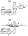
- FIG. 1 shows the structure of a receiving device in which a PIN diode is arranged in a hermetically sealed circuit module and is optically coupled to an optical fiber.
- the receiving device shown in Fig. 1 is housed in the metal housing 11, which is closed with the lid 6.
- the spacer 12 lies on the bottom of the cuboid metal housing 11.
- the spacer 12 carries the circuit module 13, which is of plate-like shape and which is arranged parallel to the bottom of the metal housing 11 at the distance predetermined by the spacer 12.
- the tube 10 In a side wall of the metal housing 11, the tube 10 is attached, which projects outwards and inwards over the side wall of the metal housing 11.
- the sleeve-shaped connecting piece 9 On the outside, the sleeve-shaped connecting piece 9 is placed on the tube 10, which is placed on the tube with the larger opening and the optical waveguide 8 is guided in its smaller opening.
- the optical waveguide 8 runs through the connector 9, the tube 10 and through the block 5 an opening in the diode carrier 3 to the optical window of the PIN photodiode 2.
- the optical fiber 8 formed by a glass fiber is fixed at two points, namely on the block 5 and inside the connector 9 at the point where the sleeve-shaped connector has the smaller inside diameter Has.
- the diode carrier 3 is fastened to the circuit module 13 with two metal angles 1.
- the two metal angles 1, of which only one is visible in FIG. 1, are located next to the PIN diode 2.
- the PIN photodiode 2 which is used has an optical window with a diameter of about 30 to 200 / um in the center of the back-side and opposite to the front side of a bonding pad.
- the optical fiber receiving module 13 is housed in a hermetically sealed, metal housing 11.
- the metal housing 11 is provided with a hermetically sealed glass fiber bushing, so that there is a so-called pigtail connection for the optical transmission.
- the hermetic encapsulation which serves for shielding and / or for corrosion protection, is particularly expedient when using unprotected semiconductor components, in particular semiconductor chips.
- the glass fiber bushing consists of the tube 10 inserted into the outer wall of the housing 11 and the connecting piece 9 placed on the tube 10.
- the optical fiber 8 is threaded through the bushing and optically coupled to the PIN photodiode 2.
- the optical fiber 8 is precisely adjusted in front of the optical window and then fixed on the block 5.
- the glass fiber is soldered into the connector 9.
- the smaller hole diameter in the connector 9 is about 120 / um larger than the diameter of the glass fiber.
- a hole diameter of about 150 microns in the connector 9 is appropriate.
- the tube 10 advantageously has a much larger inside diameter, in particular approximately> 0.5 mm.
- the connecting piece 9 has the shape of a sleeve and, as a so-called solder sleeve, ensures a transition from a large to a small diameter. It consists of two hollow cylinders with a hollow conical part in between and is provided with a solderable surface on the inside. The sleeve has approximately the same wall thickness in all areas. One hollow cylinder fits on the pipe. The glass fiber fits into the other hollow cylinder, so that there is a transition from the inside diameter of the tube to the outside diameter of the glass fiber.
- the metallization has the advantage that no alloying occurs during soldering. At the same time, it offers effective mechanical protection of the glass fiber during handling.
- the connecting piece 9 on the tube 10 is easily displaceable in the axial direction of the glass fiber 8 or in the direction of the Z axis. After the glass fiber 8 is adjusted and fixed, the connector 9 is soldered to the tube 10 without flux.
- the receiving device shown in the figures contains a PIN photodiode as the receiving diode.
- the receiving diode is used as the transmitting diode, for example a laser diode or light-emitting diode.
Landscapes
- Physics & Mathematics (AREA)
- General Physics & Mathematics (AREA)
- Optics & Photonics (AREA)
- Optical Couplings Of Light Guides (AREA)
- Measuring Pulse, Heart Rate, Blood Pressure Or Blood Flow (AREA)
- Electrotherapy Devices (AREA)
- Telephone Function (AREA)
- Light Guides In General And Applications Therefor (AREA)
- Mounting And Adjusting Of Optical Elements (AREA)
Priority Applications (1)
| Application Number | Priority Date | Filing Date | Title |
|---|---|---|---|
| AT83112093T ATE21775T1 (de) | 1982-12-03 | 1983-12-01 | Sende- und/oder empfangsvorrichtung fuer einrichtungen der elektrooptischen nachrichtenuebertragung. |
Applications Claiming Priority (2)
| Application Number | Priority Date | Filing Date | Title |
|---|---|---|---|
| DE3244867 | 1982-12-03 | ||
| DE19823244867 DE3244867A1 (de) | 1982-12-03 | 1982-12-03 | Sende- und/oder empfangsvorrichtung fuer einrichtungen der elektrooptischen nachrichtenuebertragung |
Publications (3)
| Publication Number | Publication Date |
|---|---|
| EP0111264A2 true EP0111264A2 (fr) | 1984-06-20 |
| EP0111264A3 EP0111264A3 (en) | 1984-08-08 |
| EP0111264B1 EP0111264B1 (fr) | 1986-08-27 |
Family
ID=6179780
Family Applications (1)
| Application Number | Title | Priority Date | Filing Date |
|---|---|---|---|
| EP83112093A Expired EP0111264B1 (fr) | 1982-12-03 | 1983-12-01 | Appareil de transmission ou réception pour équipement opto-électrique de communication |
Country Status (5)
| Country | Link |
|---|---|
| US (1) | US4591711A (fr) |
| EP (1) | EP0111264B1 (fr) |
| JP (1) | JPS59113408A (fr) |
| AT (1) | ATE21775T1 (fr) |
| DE (2) | DE3244867A1 (fr) |
Cited By (8)
| Publication number | Priority date | Publication date | Assignee | Title |
|---|---|---|---|---|
| EP0137485A3 (fr) * | 1983-10-12 | 1985-05-15 | Siemens Aktiengesellschaft | |
| EP0213426A1 (fr) * | 1985-08-30 | 1987-03-11 | Siemens Aktiengesellschaft | Boîtier avec une partie de fond et une couverture extérieure pour un élément de circuit électrique |
| EP0214464A1 (fr) * | 1985-09-05 | 1987-03-18 | Siemens Aktiengesellschaft | Boîtier pour un module de circuit opto-électronique |
| EP0216174A1 (fr) * | 1985-09-25 | 1987-04-01 | Siemens Aktiengesellschaft | Coupleur directif de lumière |
| DE3606588A1 (de) * | 1986-02-28 | 1987-09-03 | Siemens Ag | Gasdichte durchfuehrung einer glasfaser |
| EP0267536A3 (en) * | 1986-11-12 | 1988-10-19 | Standard Elektrik Lorenz Aktiengesellschaft | Hermetically sealed connecting passage for glass fibre |
| EP0511931A3 (en) * | 1991-04-29 | 1993-03-31 | International Business Machines Corporation | An apparatus and a method for an optical fiber interface |
| US5241614A (en) * | 1991-04-29 | 1993-08-31 | International Business Machines Corporation | Apparatus and a method for an optical fiber interface |
Families Citing this family (26)
| Publication number | Priority date | Publication date | Assignee | Title |
|---|---|---|---|---|
| DE3244882A1 (de) * | 1982-12-03 | 1984-06-07 | Siemens AG, 1000 Berlin und 8000 München | Sende- oder empfangsvorrichtung mit einer mittels eines traegers gehalterten diode |
| EP0148012B1 (fr) * | 1983-12-26 | 1988-11-02 | Kabushiki Kaisha Toshiba | Coupleur pour fibre optique |
| JPS6123379A (ja) * | 1984-07-11 | 1986-01-31 | Hitachi Ltd | 光電子装置 |
| US4726507A (en) * | 1984-08-29 | 1988-02-23 | The United States Of America As Represented By The Secretary Of The Air Force | Cryogenic glass-to-metal seal |
| DE3445982A1 (de) * | 1984-12-17 | 1986-06-19 | Siemens AG, 1000 Berlin und 8000 München | Glasfaser fuer eine optische leitung der nachrichtentechnik |
| US4722586A (en) * | 1985-04-12 | 1988-02-02 | Tektronix, Inc. | Electro-optical transducer module |
| US4814603A (en) * | 1985-06-24 | 1989-03-21 | Philips Gerald J | Method and apparatus for determining the size of defects in rolling element bearings with high frequency capability |
| DE3525480A1 (de) * | 1985-07-17 | 1987-01-29 | Kabelmetal Electro Gmbh | Verfahren zum beschichten einer glasfaser mit metall |
| US4802178A (en) * | 1986-04-10 | 1989-01-31 | Ortel Corporation | High speed fiberoptic laser module |
| US4803361A (en) * | 1986-05-26 | 1989-02-07 | Hitachi, Ltd. | Photoelectric device with optical fiber and laser emitting chip |
| DE3628391A1 (de) * | 1986-08-21 | 1988-02-25 | Licentia Gmbh | Gasdichte gehaeusedurchfuehrung fuer einen quarzglaslichtwellenleiter und verfahren zu deren herstellung |
| US5177806A (en) * | 1986-12-05 | 1993-01-05 | E. I. Du Pont De Nemours And Company | Optical fiber feedthrough |
| US4870271A (en) * | 1987-02-06 | 1989-09-26 | Philips Gerald J | Method and apparatus for determining the size of defects in rolling element bearings with high frequency capability |
| US4782226A (en) * | 1987-07-06 | 1988-11-01 | Semi-Gas Systems, Inc. | Optoelectronic chemical reaction detector |
| US4826276A (en) * | 1987-07-17 | 1989-05-02 | E. I. Du Pont De Nemours And Company | Optical fiber feedthrough assembly having a rigidizing arrangement therein |
| US4865410A (en) * | 1988-01-25 | 1989-09-12 | E. I. Du Pont De Nemours And Company | Decoupled fiber optic feedthrough assembly |
| US5011256A (en) * | 1988-10-28 | 1991-04-30 | E. I. Du Pont De Nemours And Company | Package for an opto-electronic component |
| US4979787A (en) * | 1990-01-12 | 1990-12-25 | Pco, Inc. | Optical-electronic interface module |
| JPH10319278A (ja) * | 1997-05-16 | 1998-12-04 | Nec Corp | 光結合回路 |
| US6213651B1 (en) | 1999-05-26 | 2001-04-10 | E20 Communications, Inc. | Method and apparatus for vertical board construction of fiber optic transmitters, receivers and transceivers |
| US6901221B1 (en) | 1999-05-27 | 2005-05-31 | Jds Uniphase Corporation | Method and apparatus for improved optical elements for vertical PCB fiber optic modules |
| US6325551B1 (en) | 1999-12-08 | 2001-12-04 | New Focus, Inc. | Method and apparatus for optically aligning optical fibers with optical devices |
| US6632029B1 (en) | 1999-12-22 | 2003-10-14 | New Focus, Inc. | Method & apparatus for packaging high frequency components |
| US6786652B2 (en) * | 2001-12-19 | 2004-09-07 | Northrop Grumman Corporation | Process for fabricating a photonics package and for aligning an optical fiber with a photodetector surface during fabrication of such a package |
| JP5034353B2 (ja) * | 2006-07-26 | 2012-09-26 | 富士通オプティカルコンポーネンツ株式会社 | 光デバイスの製造方法 |
| CN101697025B (zh) * | 2009-10-26 | 2012-05-30 | 西北核技术研究所 | 直通式光纤密封装置及其制造方法 |
Family Cites Families (10)
| Publication number | Priority date | Publication date | Assignee | Title |
|---|---|---|---|---|
| JPS50153650A (fr) * | 1974-05-30 | 1975-12-10 | ||
| US4118100A (en) * | 1975-12-10 | 1978-10-03 | International Telephone And Telegraph Corporation | Optical couplers for light emitting diodes and detectors |
| US4119363A (en) * | 1976-03-18 | 1978-10-10 | Bell Telephone Laboratories Incorporated | Package for optical devices including optical fiber-to-metal hermetic seal |
| US4222629A (en) * | 1978-03-27 | 1980-09-16 | Sperry Corporation | Fiber optic connector assembly |
| CA1108900A (fr) * | 1978-09-15 | 1981-09-15 | Paul P. Webb | Logement de dispositif electro-opitique pour l'usage dans l'optique des fibres |
| JPS5922203B2 (ja) * | 1978-10-06 | 1984-05-25 | ケイディディ株式会社 | 光海底中継器のフイ−ドスル |
| US4346294A (en) * | 1979-07-05 | 1982-08-24 | Burr-Brown Research Corp. | Low profile optical coupling to planar-mounted optoelectronic device |
| NL7908536A (nl) * | 1979-11-23 | 1981-06-16 | Philips Nv | Omhulling voor een fotodiode. |
| DE3010820C2 (de) * | 1980-03-20 | 1984-07-26 | Siemens AG, 1000 Berlin und 8000 München | Verfahren zur Herstellung einer Anordnung mit einer Haltevorrichtung zur Halterung eines Lichtwellenleiters |
| NL8102050A (nl) * | 1981-04-27 | 1982-11-16 | Philips Nv | Glasvezeldoorvoer in een metalen behuizing. |
-
1982
- 1982-12-03 DE DE19823244867 patent/DE3244867A1/de not_active Withdrawn
-
1983
- 1983-11-14 US US06/551,460 patent/US4591711A/en not_active Expired - Fee Related
- 1983-12-01 AT AT83112093T patent/ATE21775T1/de active
- 1983-12-01 DE DE8383112093T patent/DE3365724D1/de not_active Expired
- 1983-12-01 EP EP83112093A patent/EP0111264B1/fr not_active Expired
- 1983-12-02 JP JP58227107A patent/JPS59113408A/ja active Pending
Cited By (11)
| Publication number | Priority date | Publication date | Assignee | Title |
|---|---|---|---|---|
| EP0137485A3 (fr) * | 1983-10-12 | 1985-05-15 | Siemens Aktiengesellschaft | |
| US4707066A (en) * | 1983-10-12 | 1987-11-17 | Siemens Aktiengesellschaft | Glass fiber bushing through a wall opening of a housing and method of manufacture |
| EP0213426A1 (fr) * | 1985-08-30 | 1987-03-11 | Siemens Aktiengesellschaft | Boîtier avec une partie de fond et une couverture extérieure pour un élément de circuit électrique |
| US4763225A (en) * | 1985-08-30 | 1988-08-09 | Siemens Aktiengesellschaft | Heat dissipating housing for an electronic component |
| EP0214464A1 (fr) * | 1985-09-05 | 1987-03-18 | Siemens Aktiengesellschaft | Boîtier pour un module de circuit opto-électronique |
| US4733932A (en) * | 1985-09-05 | 1988-03-29 | Siemens Aktiengesellschaft | Housing for an optoelectronic circuit module |
| EP0216174A1 (fr) * | 1985-09-25 | 1987-04-01 | Siemens Aktiengesellschaft | Coupleur directif de lumière |
| DE3606588A1 (de) * | 1986-02-28 | 1987-09-03 | Siemens Ag | Gasdichte durchfuehrung einer glasfaser |
| EP0267536A3 (en) * | 1986-11-12 | 1988-10-19 | Standard Elektrik Lorenz Aktiengesellschaft | Hermetically sealed connecting passage for glass fibre |
| EP0511931A3 (en) * | 1991-04-29 | 1993-03-31 | International Business Machines Corporation | An apparatus and a method for an optical fiber interface |
| US5241614A (en) * | 1991-04-29 | 1993-08-31 | International Business Machines Corporation | Apparatus and a method for an optical fiber interface |
Also Published As
| Publication number | Publication date |
|---|---|
| JPS59113408A (ja) | 1984-06-30 |
| EP0111264A3 (en) | 1984-08-08 |
| ATE21775T1 (de) | 1986-09-15 |
| US4591711A (en) | 1986-05-27 |
| EP0111264B1 (fr) | 1986-08-27 |
| DE3244867A1 (de) | 1984-06-07 |
| DE3365724D1 (en) | 1986-10-02 |
Similar Documents
| Publication | Publication Date | Title |
|---|---|---|
| EP0111264B1 (fr) | Appareil de transmission ou réception pour équipement opto-électrique de communication | |
| EP0111263B1 (fr) | Appareil de transmission ou réception contenant une diode dans une monture | |
| EP1174745B1 (fr) | Module optoélectronique montable en surface | |
| DE3715417C2 (fr) | ||
| DE3822312C2 (fr) | ||
| DE69431512T2 (de) | Lichtempfängerstruktur für optische Vorrichtungen vom Wellenleitertyp | |
| WO1999062150A2 (fr) | Ensemble boitier pour module laser | |
| DE3043613A1 (de) | Umhuellung fuer eine photodiode | |
| DE69419194T2 (de) | Optoelektronisches Modul mit Kopplung zwischen einer optoelektronischen Komponente, insbesondere einem Halbleiterlaser, und einer optischen Glasfaser, und Methode seiner Herstellung | |
| DE102012223460A1 (de) | Eine modifizierte Transistor Kontur Gehäuse Baueinheit zur Verwendung in optischen Kommunikationen und ein Verfahren | |
| DE10004411A1 (de) | Elektrooptisches Sende-/Empfangsmodul und Verfahren zu seiner Herstellung | |
| DE19807536A1 (de) | Verpackungsverfahren für optische Bauteile und Kollimator-Zusammenbauverfahren | |
| DE4232327A1 (de) | Halbleiter-Lasermodul | |
| EP0267536B1 (fr) | Conduit fermé hermétiquement pour fibre en verre | |
| DE2612657A1 (de) | Stiftbefestigung fuer laser | |
| DE3338315A1 (de) | Optoelektrische koppelanordnung | |
| DE3433717C2 (fr) | ||
| DE69213778T2 (de) | Verfahren zur Herstellung eines opto-elektronischen Bauteils | |
| DE69118635T2 (de) | Optische Halbleiter-Vorrichtung | |
| DE10227544A1 (de) | Vorrichtung zur optischen und/oder elektrischen Datenübertragung und/oder -verarbeitung | |
| DE19635583A1 (de) | Optoelektronisches Sende- und/oder Empfangsmodul | |
| DE19718949A1 (de) | Elektrooptisches Modul | |
| DE19622459C1 (de) | Elektrooptisches Modul | |
| DE8234091U1 (de) | Sende- oder Empfangsvorrichtung mit einer mittels eines Trägers gehalterten Diode | |
| DE10002328B4 (de) | Optische Sende- und Empfangseinheit mit einer zwei Lichtdurchgangsöffnungen aufweisenden Montageplattform |
Legal Events
| Date | Code | Title | Description |
|---|---|---|---|
| PUAI | Public reference made under article 153(3) epc to a published international application that has entered the european phase |
Free format text: ORIGINAL CODE: 0009012 |
|
| PUAL | Search report despatched |
Free format text: ORIGINAL CODE: 0009013 |
|
| AK | Designated contracting states |
Designated state(s): AT BE CH DE FR GB IT LI NL SE |
|
| AK | Designated contracting states |
Designated state(s): AT BE CH DE FR GB IT LI NL SE |
|
| 17P | Request for examination filed |
Effective date: 19840824 |
|
| GRAA | (expected) grant |
Free format text: ORIGINAL CODE: 0009210 |
|
| AK | Designated contracting states |
Kind code of ref document: B1 Designated state(s): AT BE CH DE FR GB IT LI NL SE |
|
| REF | Corresponds to: |
Ref document number: 21775 Country of ref document: AT Date of ref document: 19860915 Kind code of ref document: T |
|
| REF | Corresponds to: |
Ref document number: 3365724 Country of ref document: DE Date of ref document: 19861002 |
|
| ET | Fr: translation filed | ||
| ITF | It: translation for a ep patent filed | ||
| PGFP | Annual fee paid to national office [announced via postgrant information from national office to epo] |
Ref country code: AT Payment date: 19861128 Year of fee payment: 4 |
|
| PLBE | No opposition filed within time limit |
Free format text: ORIGINAL CODE: 0009261 |
|
| STAA | Information on the status of an ep patent application or granted ep patent |
Free format text: STATUS: NO OPPOSITION FILED WITHIN TIME LIMIT |
|
| 26N | No opposition filed | ||
| PGFP | Annual fee paid to national office [announced via postgrant information from national office to epo] |
Ref country code: NL Payment date: 19871231 Year of fee payment: 5 |
|
| PG25 | Lapsed in a contracting state [announced via postgrant information from national office to epo] |
Ref country code: GB Effective date: 19881201 Ref country code: AT Effective date: 19881201 |
|
| PG25 | Lapsed in a contracting state [announced via postgrant information from national office to epo] |
Ref country code: LI Effective date: 19881231 Ref country code: CH Effective date: 19881231 Ref country code: BE Effective date: 19881231 |
|
| BERE | Be: lapsed |
Owner name: SIEMENS A.G. BERLIN UND MUNCHEN Effective date: 19881231 |
|
| PG25 | Lapsed in a contracting state [announced via postgrant information from national office to epo] |
Ref country code: NL Effective date: 19890701 |
|
| GBPC | Gb: european patent ceased through non-payment of renewal fee | ||
| NLV4 | Nl: lapsed or anulled due to non-payment of the annual fee | ||
| PG25 | Lapsed in a contracting state [announced via postgrant information from national office to epo] |
Ref country code: FR Free format text: LAPSE BECAUSE OF NON-PAYMENT OF DUE FEES Effective date: 19890831 |
|
| REG | Reference to a national code |
Ref country code: CH Ref legal event code: PL |
|
| PG25 | Lapsed in a contracting state [announced via postgrant information from national office to epo] |
Ref country code: DE Effective date: 19890901 |
|
| REG | Reference to a national code |
Ref country code: FR Ref legal event code: ST |
|
| PG25 | Lapsed in a contracting state [announced via postgrant information from national office to epo] |
Ref country code: SE Effective date: 19891202 |
|
| EUG | Se: european patent has lapsed |
Ref document number: 83112093.6 Effective date: 19900104 |