EP0111840A2 - Zugriffsteuerungsverfahren für Multiprozessorsysteme - Google Patents
Zugriffsteuerungsverfahren für Multiprozessorsysteme Download PDFInfo
- Publication number
- EP0111840A2 EP0111840A2 EP83112366A EP83112366A EP0111840A2 EP 0111840 A2 EP0111840 A2 EP 0111840A2 EP 83112366 A EP83112366 A EP 83112366A EP 83112366 A EP83112366 A EP 83112366A EP 0111840 A2 EP0111840 A2 EP 0111840A2
- Authority
- EP
- European Patent Office
- Prior art keywords
- bus
- data
- port
- signal
- processors
- Prior art date
- Legal status (The legal status is an assumption and is not a legal conclusion. Google has not performed a legal analysis and makes no representation as to the accuracy of the status listed.)
- Withdrawn
Links
Images


Classifications
-
- G—PHYSICS
- G06—COMPUTING OR CALCULATING; COUNTING
- G06F—ELECTRIC DIGITAL DATA PROCESSING
- G06F15/00—Digital computers in general; Data processing equipment in general
- G06F15/16—Combinations of two or more digital computers each having at least an arithmetic unit, a program unit and a register, e.g. for a simultaneous processing of several programs
- G06F15/163—Interprocessor communication
- G06F15/167—Interprocessor communication using a common memory, e.g. mailbox
-
- G—PHYSICS
- G06—COMPUTING OR CALCULATING; COUNTING
- G06F—ELECTRIC DIGITAL DATA PROCESSING
- G06F13/00—Interconnection of, or transfer of information or other signals between, memories, input/output devices or central processing units
- G06F13/14—Handling requests for interconnection or transfer
- G06F13/36—Handling requests for interconnection or transfer for access to common bus or bus system
- G06F13/368—Handling requests for interconnection or transfer for access to common bus or bus system with decentralised access control
- G06F13/37—Handling requests for interconnection or transfer for access to common bus or bus system with decentralised access control using a physical-position-dependent priority, e.g. daisy chain, round robin or token passing
Definitions
- the present invention relates to an access control method for multiprocessor systems, and more particularly to a method of controlling access to a bus or a memory, which dispenses with an exclusion control for the shared or common memory or the common bus and which can equalize the masterships of respective processors.
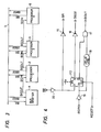
- Figure 1 is a block diagram of a prior-art multiprocessor system with a common memory.
- a plurality of processing modules (PM) 2, 3 which consist ⁇ f processors 21, 31, local memories 22, 32 and interfaces 23, 33; the common memory (CM) 1; and a bus arbiter (BA) 4 are connected through a common bus 5.
- the respective processors 21, 31 can access the common memory 1 in quite the same manner that they access the local memories 22, 32.
- FIG. 2 is a diagram showing a method for that communication between program modules which is executed in the system of Figure 1.
- the program modules 24, 34 are stored in the local memories 22, 32 within the different processing modules 2, 3, and they are executed by the corresponding processors 21, 31.
- the communication between the program modules 24, 34 is performed through common data (CD) 11 which is stored in the common memory 1. Since the common data 11 is freely accessed from either desired program module at any desired time, the versatility of the communication between the processors is very high. On the other hand, however, when a bug exists in a program, it is diffucult to detect the corresponding part so as to correct the bug.
- the common memory 1 cannot be simultaneously accessed by two or more processors.
- the bus arbiter 4 performs an exclusion control for the common bus 5 so as to prevent the simultaneous access to the common memory by the plurality of processors.
- the processor 21 or 31 has the exclusion control function of excluding the opposite processor and completely occupying the common bus 5 while the common data 11 is accessed and updated. It is true that such exclusion control is indispensable to any common memory connection method. With the prior-art method, however, a common bus occupation time required for the exclusion control is too long. Therefore, when the number of the processors is large, the common bus inoccupation-waiting time of each processor becomes very large. This results in the disadvantage of incurring increase in the overhead of the whole system.
- Figure 3 is a diagram showing a bus control method in a prior-art multiprocessor system.
- a bus arbiter 4 discriminates whether or not the bus is in the usable status, and it delivers a bus use grant signal BGOUT subject to the usable status.
- the bus use grant signal BGOUT is transmitted by the daisy chain in succession-from the processor"2 which is physically closest to the bus arbiter 4, and it is received by the processor which has provided the bus use request signal BR.
- a bus busy signal BBSY is delivered from the occupying processor.
- the bus arbiter 4 receives these signals BR and BBSY, thereby to grasp the situation of the use of the bus.
- Figure 4 is a logical structure diagram of a bus control circuit for the processor in Figure 3.
- a bus driver 15 When the processor has issued a bus use request BR, a bus driver 15 is actuated to deliver the request signal BR. Also a flip-flop F2 is set in synchronism with the reception of a use grant signal BGIN, and a bus driver 16 is actuated by the resulting set output so as to deliver the bus busy signal BBSY.
- the bus use grant signal BGIN is delivered to the succeeding processor through an inverter 19, a delay line 18 and a NAND circuit 17. More specifically, after the flip-flop F2 has been reset by the inversion of the bus use request BR, occurring when the processor has stopped using the bus, or by a reset signal RESET, the NAND circuit 17 is enabled by the resulting reset output, whereby the use grant signal BGOUT is delivered to the adjoining processor.
- each processor can freely provide the bus use request signal BR. Therefore, the processor physically closer to the bus arbiter 4 has a higher priority level for acquiring the mastership of the bus. In consequence, the processor located in a place physically remoter from the bus arbiter 4 has the bus use grant signal BGOUT blocked by the closer processor and cannot acquire the mastership. Accordingly, the bus masterships become very unequal.
- the present invention has been made in order to improve the disadvantages of the prior arts, and has for its object to provide an access control method for multiprocessor systems which can quickly detect and correct the bug of a program, which can shorten a common bus occupation time required for an exclusion control and which can equalize the bus masterships of respective processors.
- the access control method for a multiprocessor system is characterized in that a data transferring port into.which data can be written only when it is unoccupied and from which data can be read only when it has the data is provided to prevent errors which are ascribable to writing double and reading the same data twice, and to cause the port itself to perform an exclusion control operation.
- the present invention is characterized in that when a plurality of processors have simultaneously made requests for the use of a bus, one of the processors is endowed with a bus mastership, but the processor having already acquired the mastership is prevented from making the bus use request again until the use requests of the other processors run out.
- Figure 5 is a conceptual diagram of data-flow processors showing an embodiment of the present invention.
- a port (PO) 7 is just like a box which can functionally store only one data. Only when the port 7 is unoccupied, data can be written thereinto. In addition, only when one data is stored, it can be read out, whereupon the port 7 becomes unoccupied. When it is intended to read data in the unoccupied status of the port 7 or to write data in the fully'occupied status in which one data is stored, the access ends in failure.
- Figure 6 is a diagram showing a method for the communication between the processors in Figure 5.
- Program modules 24 and 34 transmit and receive common data 71 through the port 7.
- the communication in this system corresponds to transferring messages. Owing to the intervention of the port 7, data once written can be prevented from being erroneously rewritten, and an erroneous read or write operation can be quickly detected and corrected. That is, when an operation of writing or reading data has ended in failure, it can be detected as being the erroneous write or read.
- the port 7 itself has the exclusion control function, and hence, the exclusion control as required in the conventional common memory connection method is dispensed with.
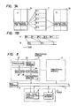
- Figures 7 A and 7B are diagrams for explaining a case where pipeline processing is performed according to Figure 6.
- Figure 7 A elucidates the operation, while Figure 7B shows a time chart.
- the program modules 24 and 34 are capable of the pipeline processing by the use of the port 7.
- the module (A) 24 includes instructions for writing data into five ports #0 - #4 in the order mentioned and where the module (B) 34 includes instructions for reading the data from the two ports #0 and #2 of the five ports, the module (B) 34 need not wait until the write instructions of the module (A) 24 end completely, but it can immediately execute the read instructions when the data of the ports #0 and #2 have been written. That is, as illustrated in Figure 7(b), after the data writing instruction of the port #2 has been started, the data read of the port #2 is started.
- Figure 8 is a setup diagram of the whole system of the data-flow processors showing an embodiment of the present invention.
- a plurality of processing modules 2 each of which consists of a processor 21, a local memory 22, a buffer 27, a controller 25 and a distributed arbiter 26; a bus arbiter 4; and a port 7 which consists of a common memory 1 and a data flow controlling module 8 are connected through a common bus 5.
- the respective processors can write data into the common memory 1 of the port 7 or read data therefrom.
- the data flow controlling module 8 manages the operation so that.data once written may not be erroneously rewritten and that an erroneous read or write operation may be quickly detected.
- the buffer 27, controller 25 and distributed arbiter 26 are arranged instead of the foregoing interface 23, so as to perform a more delicate control owing to functions distributed thereto.
- Figure 9 is a block diagram of the data flow controlling module in Figure 8.
- This module 8 has one bit of status information every byte of the common memory 1.
- the status information indicates whether the port 7 is in the unoccupied status ("0") or in the fully occupied status ("I").
- the status information is inverted, and a data strobe signal LDS, UDS is delivered from this module 8 to the common memory (MEM) 1, depending upon a data strobe signal DSO, DS1 on the common bus (BUS) 5.
- the signal LDS, UDS is not provided, and the access of the data itself is not performed. Instead, a signal NACK, which indicates that the access has ended in failure, is delivered to the processing module which has intended the access. In this case, the status information does not change.
- the data flow controlling module 8 is constructed of an address decoding circuit 9, a status circuit 10, an output signal distributing circuit 11 and an initializing circuit 12. Next, these circuits will be described.
- Figure 10 is a block circuit of the address decoding circuit in Figure 9 .
- This circuit generates a signal CS which indicates that an address area supported by the data flow controlling module 8 has been accessed; signals CS100, CS140 and CS160 which are respectively delayed by fixed times; and signals CSOL, CS1L, CSOU and CS1U which select memories in the status circuit 10 for storing the status information.
- CS CS which indicates that an address area supported by the data flow controlling module 8 has been accessed
- signals CS100, CS140 and CS160 which are respectively delayed by fixed times
- signals CSOL, CS1L, CSOU and CS1U which select memories in the status circuit 10 for storing the status information.
- a comparator circuit 91 compares the address AO - A7 of the common memory 1 and an accessed address A16 - A23 (BO - B7). When they have agreed, it supplies the common memory 1 with the chip select signal CS and also supplies the status circuit 10 with the signal CSOL, CS1L, CSOU or CS1U.
- the addresses of the common memory 1 can be determined at will with an address setting switch 92. For example, in a case where, among addresses 0 - 10000, a range of addresses 2000 - 3000 is desired to be used as the objects of the ports, the addresses AO - A7 are set at this range by the address setting switch 92.
- the memory addresses to be accessed are divided into upper addresses AO - A15 and lower addresses A16 - A23, and only the lower addresses A16 - A23 are compared and checked in the address decoding circuit 9.
- Figure 11 is a block diagram of the status circuit in Figure 9.
- the status circuit 10 manages the status information of the respective ports, and decides the propriety of access.
- Each port is assigned one bit, the value "0" of which indicates the unoccupied status of the port and the value "1" of which indicates the fully occupied status.
- a signal NACKOL, NACKlL, NACKOU or NACKlU becomes “0" only when the status of the port coincides with the access content and the port access fails.
- This signal is supplied to a flip-flop Fl through a gate Gl. Meanwhile, the signal CS100 delayed by 100 ns is used as the clock signal of the flip-flop Fl, to ensure that the signal NACKOL - NACKIU be latched in the flip-flop Fl in the definite state thereof.
- This output signal NACK is supplied'to the output signal distributing circuit 11, and is also supplied to the write enable terminal WE of the RAM 1030 through a gate G3.
- this signal becomes "0", and the signal "0" enters the RAM 1030, so that the status information of the corresponding port is inverted.
- the signal CS140 is applied to the gate G3 in order to ensure that the above signal be definite.
- an output terminal Dout becomes a high impedance, and hence, the flip-flop Fl is used so that the status at the starting of the access can be correctly held.
- the status circuit 10 is divided into four parts 101 - 104 enclosed with dotted lines, among which the circuits 101 and 102 check the statuses of the lower addresses, while the circuits 103 and 104 check the statuses of the upper addresses. Excepting the addresses to be applied and the chip select signals CSOL, 1L, OU and lU, the four parts are constructed of quite the same circuit arrangement.
- the RAM 1030 is supplied with the chip select signal CSOU from tne address decoding circuit 9, with a read/write signal R/ W and address A14 - Al from the bus, and with the write enable signal WE from tne NAND circuit G3.
- a gate circuit is not enabled by the output D out of the RAM 1030 and the output R/ W , and the gate Gl is supplied with "0".
- Figure 12 is a logical structure diagram of the initializing circuit in Figure 9.
- the status information of the ports are still undefined.
- the output INIT of the flip-flop F3 of the initializing circuit 12 is rendered "0", whereby all the ports are made accessible irrespective of the contents of the status information.
- the signal INIT is applied to the gate G2 of the status circuit 10. Therefore, when the above signal is "0", the output of the gate G2 becomes ''0" irrespective of the signals NACKOL - NACKlU, and the ports become accessible. Then, all the ports supported by the data flow controlling module 8 are subjected to read operations by a system initializing program, thereby to bring the ports into the unoccupied statuses.
- Figure 13 is a logical structure diagram of the output signal distributing circuit in Figure 9.
- the output signal distributing circuit 11 generates the signal NACK to be finally sent back to the processing modules 2, 3 and the signals LDS, UDS to be delivered to the common memory 1, on the basis of the output NACK of the gate G2 and the data strobe signal DSO, DS1.
- the signals CS140 and CS160 applied to the gates G5, G6 serve to ensure the settlement of the signal -NACK and to prevent the occurrence of hazards in an access grant cycle.
- any form may of course be employed as long as it realizes the idea of the ports stated above.
- 128 k ports can be supported.
- a different kind of RAM device for example, one of 1 k x 1 bits or 4 k x 1 bits, or a dynamic memory device or the like.
- the memory must be rewritable.
- the data strobe signals LDS, UDS may well be replaced with one signal or at least three signals.
- the two sorts of signals NACK (LDS, UDS) and the timing signal associated with the rewriting of the status information can take other forms.
- Figure 14 is an arrangement diagram of a bus control circuit for the processing module showing an embodiment of the present invention.
- the bus control is performed by the distributed arbiter 26.
- a distributed arbiter in Figure 14 produces the bus use request signal BR on the basis of the signal NACK provided from the port 7 in Figure 8, and the same port can be accessed again.
- the respective processors can freely provide the bus use request signals BR.
- the bus control circuit shown in Figure 14 checks the bus use request of the other processor and the status of the bus so as to control the delivery of the bus use request signal. That is, once the processor has used the bus, this processor having used the bus cannot request the use of the bus again until the status is established in which the bus use request signal of the other processor is not provided and in which the bus is not used, in order to give priority to the use of the bus by the other processor providing the bus use request. In this way, the bus masterships of the respective processors are equalized.
- the bus control circuit shown in Figure 14 has a circuit added to the conventional circuit shown in Figure 4, the added circuit is as follows.
- the output side signals of the bus drivers 15, 16 for the bus use request signal BR and the bus busy signal BBSY are used as the inputs of a NAND circuit 14, the output of which is used as the clear input of a flip-flop F4.
- the output Q of the flip-flop F4 controls whether or not the bus request BRfrcm the processor can be delivered to the bus as the signal BR.
- the bus control circuit of any distributed arbiter does not produce the bus use request signal BR, and the bus 5 is in the unoccupied status, so that the NAND circuit 14 delivers a low output level to the clear input terminal CLR of the flip-flop F4.
- the flip-flop F4 is reset to provide a low level output from the output terminal Q.
- tne processor brings the signal BR toward the distributed bus arbiter into its low level with the intention of making the bus use request
- a NAND circuit 13 provides a high level output, and the bus use request signal BR can be delivered to the bus. Owing to the delivery of the request signal BR, the bus arbiter 4 is actuated, and the bus use grant signal BGIN is received via the daisy chain.
- This grant signal BGIN is applied to the clock input terminal CK of a flip-flop F2 through an inverter 19. Then, since high level voltages are applied to the PR input terminal and CLR input terminal of the flip-flop F2 and the clock is valid at that time, a high level voltage and a low level voltage are respectively provided from the output Q and output Q of the flip-flop F2.
- the high level voltage from the output Q delivers the bus busy signal BBSY to the bus via the bus driver 16, and the bus is occupied.
- the high level output voltage of the output Q of the flip-flop F2 is applied to the clock input terminal CLK of the flip-flop F4, thereby to apply a high level voltage from the output Q of the flip-flop F4 to the NAND circuit 13.
- the use of the bus is ended. Even when the signal BR is brought into its low level again with the intention of making the request for the use of the bus, the inputs of the NAND circuit 13 are not satisfied because of the high level of the output Q of the flip-flop F4, and the bus use request signal BR cannot be delivered onto the bus. In order to deliver the signal BR to tne bus, the flip-flop F4 must be reset with its output 0 held at the low level. The flip-flop F4 is reset in the status in which the signals BR and BBSY are not on the bus.
- the bus use requests of the other processors are successively granted by the bus arbiter 4, the use of the bus ends entirely, the signals BR and BBSY become the high level, and the low level voltage is applied from the NAND circuit 14 to the input terminal CLR of the flip-flop F4, whereby the flip-flop F4 is reset. Owing to the resetting of the flip-flop F4, the low level voltage is applied from the output Q to the NAND circuit 13.
- the signal BR becomes the low level
- AND conditions are satisfied, and the output of the NAND circuit 13 becomes the high level. Therefore, it becomes possible to provide the signal BR.
- the bus use grant signal BGIN has been received in the status in which the signal BR is not provided, it is decided whether or not the-signal BR is being provided.
- the signal BGOUT is delivered in order to apply it as the use grant signal BGIN of the next processor.
- a delay line 18 affords a delay required for deciding whether or not the signal BR is being provided, and a delay time not shorter than the operating time of the flip-flop F2.is necessary.
- bus masterships of the respective processors constituting the multiple microprocessor system can be equalized.
- a port is provided as a common memory, so that in transferring data between processors, errors attributed to writing data double into an identical area and reading identical data twice can be detected and prevented, and that the port itself possesses an exclusion control function, whereby the exclusion control having been required in the common connection method is dispensed with, and a common bus occupation time necessary for the exclusion control can be shortened.
- the respective processors are furnished with bus control circuits, so that the masterships of the respective processors for a common bus can be equalized, and the throughput of the whole system can be enhanced.
Landscapes
- Engineering & Computer Science (AREA)
- Theoretical Computer Science (AREA)
- Physics & Mathematics (AREA)
- General Engineering & Computer Science (AREA)
- General Physics & Mathematics (AREA)
- Computer Hardware Design (AREA)
- Software Systems (AREA)
- Multi Processors (AREA)
- Memory System (AREA)
- Information Transfer Systems (AREA)
Applications Claiming Priority (2)
| Application Number | Priority Date | Filing Date | Title |
|---|---|---|---|
| JP57221684A JPS59111561A (ja) | 1982-12-17 | 1982-12-17 | 複合プロセツサ・システムのアクセス制御方式 |
| JP221684/82 | 1982-12-17 |
Publications (2)
| Publication Number | Publication Date |
|---|---|
| EP0111840A2 true EP0111840A2 (de) | 1984-06-27 |
| EP0111840A3 EP0111840A3 (de) | 1986-12-30 |
Family
ID=16770651
Family Applications (1)
| Application Number | Title | Priority Date | Filing Date |
|---|---|---|---|
| EP83112366A Withdrawn EP0111840A3 (de) | 1982-12-17 | 1983-12-08 | Zugriffsteuerungsverfahren für Multiprozessorsysteme |
Country Status (3)
| Country | Link |
|---|---|
| US (1) | US4571672A (de) |
| EP (1) | EP0111840A3 (de) |
| JP (1) | JPS59111561A (de) |
Cited By (1)
| Publication number | Priority date | Publication date | Assignee | Title |
|---|---|---|---|---|
| EP0234182A1 (de) * | 1986-02-24 | 1987-09-02 | International Business Machines Corporation | Ein Multiprozessordatenverarbeitungssystem |
Families Citing this family (124)
| Publication number | Priority date | Publication date | Assignee | Title |
|---|---|---|---|---|
| KR900002438B1 (ko) * | 1984-02-29 | 1990-04-14 | 가부시끼가이샤 도오시바 | 프로세서간 결합방식 |
| US4760521A (en) * | 1985-11-18 | 1988-07-26 | White Consolidated Industries, Inc. | Arbitration system using centralized and decentralized arbitrators to access local memories in a multi-processor controlled machine tool |
| GB2196762B (en) * | 1986-10-27 | 1990-12-19 | Burr Brown Ltd | Interleaved access to global memory by high priority source |
| GB2197506A (en) * | 1986-10-27 | 1988-05-18 | Burr Brown Ltd | Providing and handling break points in a software monitor |
| JPS63199540A (ja) * | 1987-02-16 | 1988-08-18 | Toshiba Corp | デ−タ伝送方法及び装置 |
| US4947368A (en) * | 1987-05-01 | 1990-08-07 | Digital Equipment Corporation | Lookahead bus arbitration system with override of conditional access grants by bus cycle extensions for multicycle data transfers |
| US5111424A (en) * | 1987-05-01 | 1992-05-05 | Digital Equipment Corporation | Lookahead bus arbitration system with override of conditional access grants by bus cycle extensions for multicycle data transfer |
| US4980854A (en) * | 1987-05-01 | 1990-12-25 | Digital Equipment Corporation | Lookahead bus arbitration system with override of conditional access grants by bus cycle extensions for multicycle data transfers |
| US5034883A (en) * | 1987-05-01 | 1991-07-23 | Digital Equipment Corporation | Lockhead bus arbitration system with override of conditional access grants by bus cycle extensions for multicycle data transfers |
| US5257392A (en) * | 1988-01-29 | 1993-10-26 | Sharp Kabushiki Kaisha | System for loading and dumping data in a data flow processor based on paired program data and data to be processed |
| US5003464A (en) * | 1988-05-23 | 1991-03-26 | Bell Communications Research, Inc. | Methods and apparatus for efficient resource allocation |
| US5210828A (en) * | 1988-12-29 | 1993-05-11 | International Business Machines Corporation | Multiprocessing system with interprocessor communications facility |
| US5168568A (en) * | 1989-02-06 | 1992-12-01 | Compaq Computer Corporation | Delaying arbitration of bus access in digital computers |
| DE69030640T2 (de) * | 1989-11-03 | 1997-11-06 | Compaq Computer Corp | Multiprozessorarbitrierung in für Einzelprozessor bestimmten Arbitrierungsschemas |
| US5206948A (en) * | 1989-12-22 | 1993-04-27 | Bull Hn Information Systems Inc. | Bus monitor with means for selectively capturing trigger conditions |
| US6751696B2 (en) | 1990-04-18 | 2004-06-15 | Rambus Inc. | Memory device having a programmable register |
| IL96808A (en) * | 1990-04-18 | 1996-03-31 | Rambus Inc | Introductory / Origin Circuit Agreed Using High-Performance Brokerage |
| US5995443A (en) * | 1990-04-18 | 1999-11-30 | Rambus Inc. | Synchronous memory device |
| US5269013A (en) * | 1991-03-20 | 1993-12-07 | Digital Equipment Corporation | Adaptive memory management method for coupled memory multiprocessor systems |
| US5303362A (en) * | 1991-03-20 | 1994-04-12 | Digital Equipment Corporation | Coupled memory multiprocessor computer system including cache coherency management protocols |
| US5450546A (en) * | 1992-01-31 | 1995-09-12 | Adaptec, Inc. | Intelligent hardware for automatically controlling buffer memory storage space in a disk drive |
| US5463753A (en) * | 1992-10-02 | 1995-10-31 | Compaq Computer Corp. | Method and apparatus for reducing non-snoop window of a cache controller by delaying host bus grant signal to the cache controller |
| US5535395A (en) * | 1992-10-02 | 1996-07-09 | Compaq Computer Corporation | Prioritization of microprocessors in multiprocessor computer systems |
| US5553310A (en) * | 1992-10-02 | 1996-09-03 | Compaq Computer Corporation | Split transactions and pipelined arbitration of microprocessors in multiprocessing computer systems |
| US5353415A (en) * | 1992-10-02 | 1994-10-04 | Compaq Computer Corporation | Method and apparatus for concurrency of bus operations |
| US5553248A (en) * | 1992-10-02 | 1996-09-03 | Compaq Computer Corporation | System for awarding the highest priority to a microprocessor releasing a system bus after aborting a locked cycle upon detecting a locked retry signal |
| JP2936036B2 (ja) * | 1992-10-27 | 1999-08-23 | 富士通株式会社 | メモリアクセス装置 |
| US6349371B1 (en) * | 1999-10-01 | 2002-02-19 | Stmicroelectronics Ltd. | Circuit for storing information |
| US7356817B1 (en) | 2000-03-31 | 2008-04-08 | Intel Corporation | Real-time scheduling of virtual machines |
| US6754815B1 (en) | 2000-03-31 | 2004-06-22 | Intel Corporation | Method and system for scrubbing an isolated area of memory after reset of a processor operating in isolated execution mode if a cleanup flag is set |
| US6769058B1 (en) | 2000-03-31 | 2004-07-27 | Intel Corporation | Resetting a processor in an isolated execution environment |
| US6957332B1 (en) | 2000-03-31 | 2005-10-18 | Intel Corporation | Managing a secure platform using a hierarchical executive architecture in isolated execution mode |
| US7194634B2 (en) | 2000-03-31 | 2007-03-20 | Intel Corporation | Attestation key memory device and bus |
| US6795905B1 (en) | 2000-03-31 | 2004-09-21 | Intel Corporation | Controlling accesses to isolated memory using a memory controller for isolated execution |
| US7111176B1 (en) | 2000-03-31 | 2006-09-19 | Intel Corporation | Generating isolated bus cycles for isolated execution |
| US7089418B1 (en) | 2000-03-31 | 2006-08-08 | Intel Corporation | Managing accesses in a processor for isolated execution |
| US6678825B1 (en) | 2000-03-31 | 2004-01-13 | Intel Corporation | Controlling access to multiple isolated memories in an isolated execution environment |
| US6934817B2 (en) * | 2000-03-31 | 2005-08-23 | Intel Corporation | Controlling access to multiple memory zones in an isolated execution environment |
| US7073071B1 (en) | 2000-03-31 | 2006-07-04 | Intel Corporation | Platform and method for generating and utilizing a protected audit log |
| US7082615B1 (en) | 2000-03-31 | 2006-07-25 | Intel Corporation | Protecting software environment in isolated execution |
| US7013481B1 (en) | 2000-03-31 | 2006-03-14 | Intel Corporation | Attestation key memory device and bus |
| US6990579B1 (en) | 2000-03-31 | 2006-01-24 | Intel Corporation | Platform and method for remote attestation of a platform |
| US6760441B1 (en) | 2000-03-31 | 2004-07-06 | Intel Corporation | Generating a key hieararchy for use in an isolated execution environment |
| US7013484B1 (en) | 2000-03-31 | 2006-03-14 | Intel Corporation | Managing a secure environment using a chipset in isolated execution mode |
| DE10030158A1 (de) * | 2000-06-20 | 2002-01-03 | Bayerische Motoren Werke Ag | Steuergerät mit einem Hauptmikroprozessor und mit einer Prozessorschnittstelle zu einer Bus-Sende-Empfangseinheit |
| US6976162B1 (en) * | 2000-06-28 | 2005-12-13 | Intel Corporation | Platform and method for establishing provable identities while maintaining privacy |
| US7793111B1 (en) * | 2000-09-28 | 2010-09-07 | Intel Corporation | Mechanism to handle events in a machine with isolated execution |
| US7389427B1 (en) | 2000-09-28 | 2008-06-17 | Intel Corporation | Mechanism to secure computer output from software attack using isolated execution |
| US7215781B2 (en) * | 2000-12-22 | 2007-05-08 | Intel Corporation | Creation and distribution of a secret value between two devices |
| US7035963B2 (en) * | 2000-12-27 | 2006-04-25 | Intel Corporation | Method for resolving address space conflicts between a virtual machine monitor and a guest operating system |
| US7818808B1 (en) | 2000-12-27 | 2010-10-19 | Intel Corporation | Processor mode for limiting the operation of guest software running on a virtual machine supported by a virtual machine monitor |
| US7225441B2 (en) | 2000-12-27 | 2007-05-29 | Intel Corporation | Mechanism for providing power management through virtualization |
| US6907600B2 (en) | 2000-12-27 | 2005-06-14 | Intel Corporation | Virtual translation lookaside buffer |
| US7117376B2 (en) * | 2000-12-28 | 2006-10-03 | Intel Corporation | Platform and method of creating a secure boot that enforces proper user authentication and enforces hardware configurations |
| US20020144121A1 (en) * | 2001-03-30 | 2002-10-03 | Ellison Carl M. | Checking file integrity using signature generated in isolated execution |
| US7096497B2 (en) | 2001-03-30 | 2006-08-22 | Intel Corporation | File checking using remote signing authority via a network |
| US7191440B2 (en) * | 2001-08-15 | 2007-03-13 | Intel Corporation | Tracking operating system process and thread execution and virtual machine execution in hardware or in a virtual machine monitor |
| US7024555B2 (en) | 2001-11-01 | 2006-04-04 | Intel Corporation | Apparatus and method for unilaterally loading a secure operating system within a multiprocessor environment |
| US20030126454A1 (en) * | 2001-12-28 | 2003-07-03 | Glew Andrew F. | Authenticated code method and apparatus |
| US7308576B2 (en) | 2001-12-31 | 2007-12-11 | Intel Corporation | Authenticated code module |
| US6959372B1 (en) * | 2002-02-19 | 2005-10-25 | Cogent Chipware Inc. | Processor cluster architecture and associated parallel processing methods |
| US7085866B1 (en) * | 2002-02-19 | 2006-08-01 | Hobson Richard F | Hierarchical bus structure and memory access protocol for multiprocessor systems |
| US7480806B2 (en) * | 2002-02-22 | 2009-01-20 | Intel Corporation | Multi-token seal and unseal |
| US7631196B2 (en) | 2002-02-25 | 2009-12-08 | Intel Corporation | Method and apparatus for loading a trustable operating system |
| US7028149B2 (en) * | 2002-03-29 | 2006-04-11 | Intel Corporation | System and method for resetting a platform configuration register |
| US7069442B2 (en) | 2002-03-29 | 2006-06-27 | Intel Corporation | System and method for execution of a secured environment initialization instruction |
| US20030191943A1 (en) * | 2002-04-05 | 2003-10-09 | Poisner David I. | Methods and arrangements to register code |
| US20030196096A1 (en) * | 2002-04-12 | 2003-10-16 | Sutton James A. | Microcode patch authentication |
| US7076669B2 (en) | 2002-04-15 | 2006-07-11 | Intel Corporation | Method and apparatus for communicating securely with a token |
| US7058807B2 (en) * | 2002-04-15 | 2006-06-06 | Intel Corporation | Validation of inclusion of a platform within a data center |
| US7127548B2 (en) * | 2002-04-16 | 2006-10-24 | Intel Corporation | Control register access virtualization performance improvement in the virtual-machine architecture |
| US7139890B2 (en) * | 2002-04-30 | 2006-11-21 | Intel Corporation | Methods and arrangements to interface memory |
| US20030229794A1 (en) * | 2002-06-07 | 2003-12-11 | Sutton James A. | System and method for protection against untrusted system management code by redirecting a system management interrupt and creating a virtual machine container |
| US6820177B2 (en) | 2002-06-12 | 2004-11-16 | Intel Corporation | Protected configuration space in a protected environment |
| US7142674B2 (en) * | 2002-06-18 | 2006-11-28 | Intel Corporation | Method of confirming a secure key exchange |
| US7392415B2 (en) * | 2002-06-26 | 2008-06-24 | Intel Corporation | Sleep protection |
| US20040003321A1 (en) * | 2002-06-27 | 2004-01-01 | Glew Andrew F. | Initialization of protected system |
| US7124327B2 (en) * | 2002-06-29 | 2006-10-17 | Intel Corporation | Control over faults occurring during the operation of guest software in the virtual-machine architecture |
| US6996748B2 (en) * | 2002-06-29 | 2006-02-07 | Intel Corporation | Handling faults associated with operation of guest software in the virtual-machine architecture |
| US7296267B2 (en) * | 2002-07-12 | 2007-11-13 | Intel Corporation | System and method for binding virtual machines to hardware contexts |
| US7165181B2 (en) * | 2002-11-27 | 2007-01-16 | Intel Corporation | System and method for establishing trust without revealing identity |
| US20040117532A1 (en) * | 2002-12-11 | 2004-06-17 | Bennett Steven M. | Mechanism for controlling external interrupts in a virtual machine system |
| US7073042B2 (en) * | 2002-12-12 | 2006-07-04 | Intel Corporation | Reclaiming existing fields in address translation data structures to extend control over memory accesses |
| US7318235B2 (en) * | 2002-12-16 | 2008-01-08 | Intel Corporation | Attestation using both fixed token and portable token |
| US20040117318A1 (en) * | 2002-12-16 | 2004-06-17 | Grawrock David W. | Portable token controlling trusted environment launch |
| US7318141B2 (en) | 2002-12-17 | 2008-01-08 | Intel Corporation | Methods and systems to control virtual machines |
| US7793286B2 (en) * | 2002-12-19 | 2010-09-07 | Intel Corporation | Methods and systems to manage machine state in virtual machine operations |
| US7900017B2 (en) * | 2002-12-27 | 2011-03-01 | Intel Corporation | Mechanism for remapping post virtual machine memory pages |
| US20040128345A1 (en) * | 2002-12-27 | 2004-07-01 | Robinson Scott H. | Dynamic service registry |
| US20040128465A1 (en) * | 2002-12-30 | 2004-07-01 | Lee Micheil J. | Configurable memory bus width |
| US7076802B2 (en) * | 2002-12-31 | 2006-07-11 | Intel Corporation | Trusted system clock |
| US7415708B2 (en) * | 2003-06-26 | 2008-08-19 | Intel Corporation | Virtual machine management using processor state information |
| US20050044292A1 (en) * | 2003-08-19 | 2005-02-24 | Mckeen Francis X. | Method and apparatus to retain system control when a buffer overflow attack occurs |
| US7287197B2 (en) * | 2003-09-15 | 2007-10-23 | Intel Corporation | Vectoring an interrupt or exception upon resuming operation of a virtual machine |
| US7424709B2 (en) * | 2003-09-15 | 2008-09-09 | Intel Corporation | Use of multiple virtual machine monitors to handle privileged events |
| US7739521B2 (en) * | 2003-09-18 | 2010-06-15 | Intel Corporation | Method of obscuring cryptographic computations |
| US7610611B2 (en) * | 2003-09-19 | 2009-10-27 | Moran Douglas R | Prioritized address decoder |
| US7237051B2 (en) * | 2003-09-30 | 2007-06-26 | Intel Corporation | Mechanism to control hardware interrupt acknowledgement in a virtual machine system |
| US7177967B2 (en) * | 2003-09-30 | 2007-02-13 | Intel Corporation | Chipset support for managing hardware interrupts in a virtual machine system |
| US20050080934A1 (en) | 2003-09-30 | 2005-04-14 | Cota-Robles Erik C. | Invalidating translation lookaside buffer entries in a virtual machine (VM) system |
| US7366305B2 (en) * | 2003-09-30 | 2008-04-29 | Intel Corporation | Platform and method for establishing trust without revealing identity |
| US7636844B2 (en) * | 2003-11-17 | 2009-12-22 | Intel Corporation | Method and system to provide a trusted channel within a computer system for a SIM device |
| US20050108534A1 (en) * | 2003-11-19 | 2005-05-19 | Bajikar Sundeep M. | Providing services to an open platform implementing subscriber identity module (SIM) capabilities |
| US8156343B2 (en) | 2003-11-26 | 2012-04-10 | Intel Corporation | Accessing private data about the state of a data processing machine from storage that is publicly accessible |
| US8037314B2 (en) * | 2003-12-22 | 2011-10-11 | Intel Corporation | Replacing blinded authentication authority |
| US20050133582A1 (en) * | 2003-12-22 | 2005-06-23 | Bajikar Sundeep M. | Method and apparatus for providing a trusted time stamp in an open platform |
| US20050152539A1 (en) * | 2004-01-12 | 2005-07-14 | Brickell Ernie F. | Method of protecting cryptographic operations from side channel attacks |
| US7802085B2 (en) | 2004-02-18 | 2010-09-21 | Intel Corporation | Apparatus and method for distributing private keys to an entity with minimal secret, unique information |
| US20050216920A1 (en) * | 2004-03-24 | 2005-09-29 | Vijay Tewari | Use of a virtual machine to emulate a hardware device |
| US7356735B2 (en) * | 2004-03-30 | 2008-04-08 | Intel Corporation | Providing support for single stepping a virtual machine in a virtual machine environment |
| US7620949B2 (en) | 2004-03-31 | 2009-11-17 | Intel Corporation | Method and apparatus for facilitating recognition of an open event window during operation of guest software in a virtual machine environment |
| US7490070B2 (en) | 2004-06-10 | 2009-02-10 | Intel Corporation | Apparatus and method for proving the denial of a direct proof signature |
| US20050288056A1 (en) * | 2004-06-29 | 2005-12-29 | Bajikar Sundeep M | System including a wireless wide area network (WWAN) module with an external identity module reader and approach for certifying the WWAN module |
| US7305592B2 (en) * | 2004-06-30 | 2007-12-04 | Intel Corporation | Support for nested fault in a virtual machine environment |
| US7840962B2 (en) * | 2004-09-30 | 2010-11-23 | Intel Corporation | System and method for controlling switching between VMM and VM using enabling value of VMM timer indicator and VMM timer value having a specified time |
| US8146078B2 (en) | 2004-10-29 | 2012-03-27 | Intel Corporation | Timer offsetting mechanism in a virtual machine environment |
| US8924728B2 (en) * | 2004-11-30 | 2014-12-30 | Intel Corporation | Apparatus and method for establishing a secure session with a device without exposing privacy-sensitive information |
| US8533777B2 (en) * | 2004-12-29 | 2013-09-10 | Intel Corporation | Mechanism to determine trust of out-of-band management agents |
| US8279886B2 (en) * | 2004-12-30 | 2012-10-02 | Intel Corporation | Dataport and methods thereof |
| US7395405B2 (en) * | 2005-01-28 | 2008-07-01 | Intel Corporation | Method and apparatus for supporting address translation in a virtual machine environment |
| US7809957B2 (en) | 2005-09-29 | 2010-10-05 | Intel Corporation | Trusted platform module for generating sealed data |
| US8014530B2 (en) | 2006-03-22 | 2011-09-06 | Intel Corporation | Method and apparatus for authenticated, recoverable key distribution with no database secrets |
| DE102007063291A1 (de) * | 2007-12-27 | 2009-07-02 | Robert Bosch Gmbh | Sicherheitssteuerung |
| US8514855B1 (en) * | 2010-05-04 | 2013-08-20 | Sandia Corporation | Extensible packet processing architecture |
Family Cites Families (3)
| Publication number | Priority date | Publication date | Assignee | Title |
|---|---|---|---|---|
| US4285038A (en) * | 1976-10-15 | 1981-08-18 | Tokyo Shibaura Electric Co., Ltd. | Information transfer control system |
| GB1601955A (en) * | 1977-10-21 | 1981-11-04 | Marconi Co Ltd | Data processing systems |
| GB1601956A (en) * | 1978-03-02 | 1981-11-04 | Marconi Co Ltd | Multiprocessor data processing systems |
-
1982
- 1982-12-17 JP JP57221684A patent/JPS59111561A/ja active Pending
-
1983
- 1983-12-08 EP EP83112366A patent/EP0111840A3/de not_active Withdrawn
- 1983-12-19 US US06/563,038 patent/US4571672A/en not_active Expired - Lifetime
Cited By (1)
| Publication number | Priority date | Publication date | Assignee | Title |
|---|---|---|---|---|
| EP0234182A1 (de) * | 1986-02-24 | 1987-09-02 | International Business Machines Corporation | Ein Multiprozessordatenverarbeitungssystem |
Also Published As
| Publication number | Publication date |
|---|---|
| US4571672A (en) | 1986-02-18 |
| JPS59111561A (ja) | 1984-06-27 |
| EP0111840A3 (de) | 1986-12-30 |
Similar Documents
| Publication | Publication Date | Title |
|---|---|---|
| US4571672A (en) | Access control method for multiprocessor systems | |
| CA1254663A (en) | Multiprocessor system architecture | |
| US4158235A (en) | Multi port time-shared associative buffer storage pool | |
| US4156932A (en) | Programmable communications controller | |
| US4212057A (en) | Shared memory multi-microprocessor computer system | |
| US4571676A (en) | Memory module selection and reconfiguration apparatus in a data processing system | |
| US4964038A (en) | Data processing system having automatic address allocation arrangements for addressing interface cards | |
| US4404628A (en) | Multiprocessor system | |
| FI92262C (fi) | Joustava väyläjärjestelmä | |
| US3761879A (en) | Bus transport system for selection information and data | |
| CA1189978A (en) | Interchangeable interface circuitry arrangements for use with a data processing system | |
| KR100227419B1 (ko) | 외부기억장치 및 그의 메모리 액세스 제어방법 | |
| US5666515A (en) | Information processing system having multiple modules and a memory on a bus, where any module can lock an addressable portion of the memory by sending retry signals to other modules that try to read at the locked address | |
| JPS61109164A (ja) | バス制御方法 | |
| GB2089076A (en) | Data proccessing system | |
| US4611275A (en) | Time sharing device for access to a main memory through to a single bus connected between a central computer and a plurality of peripheral computers | |
| HK18590A (en) | Extended addressing apparatus and method for direct storage access devices | |
| EP0051426A1 (de) | Warteschlangen-Anforderungsspeicherung in einer Speichersteuerung | |
| US5301332A (en) | Method and apparatus for a dynamic, timed-loop arbitration | |
| FI74158C (fi) | Kopplingsanordning foer givande av styrorder i ett mikrocomputersystem. | |
| US6308244B1 (en) | Information processing apparatus with improved multiple memory access and control | |
| EP0265575A1 (de) | Datenverarbeitungsanordnung mit Vorrichtungen zur automatischen Adresszuordnung zur Adressierung von Schnittstellenmodulen | |
| US5436856A (en) | Self testing computer system with circuits including test registers | |
| US6820158B1 (en) | Method and apparatus for a configuration ring | |
| WO1981002798A1 (en) | Computer system and interface therefor |
Legal Events
| Date | Code | Title | Description |
|---|---|---|---|
| PUAI | Public reference made under article 153(3) epc to a published international application that has entered the european phase |
Free format text: ORIGINAL CODE: 0009012 |
|
| AK | Designated contracting states |
Designated state(s): DE FR GB NL |
|
| 17P | Request for examination filed |
Effective date: 19840516 |
|
| PUAL | Search report despatched |
Free format text: ORIGINAL CODE: 0009013 |
|
| AK | Designated contracting states |
Kind code of ref document: A3 Designated state(s): DE FR GB NL |
|
| STAA | Information on the status of an ep patent application or granted ep patent |
Free format text: STATUS: THE APPLICATION IS DEEMED TO BE WITHDRAWN |
|
| 18D | Application deemed to be withdrawn |
Effective date: 19870701 |
|
| RIN1 | Information on inventor provided before grant (corrected) |
Inventor name: ISHIDA, HIDEAKI Inventor name: HATADA, MINORU Inventor name: MATSUSHITA, MASATOSHI |