EP0112227A2 - Einrichtung zum Unterdrücken von Auswirkungen der thermischen Zeitkonstanten bei einer Anordnung mit lichtemittierender Diode - Google Patents
Einrichtung zum Unterdrücken von Auswirkungen der thermischen Zeitkonstanten bei einer Anordnung mit lichtemittierender Diode Download PDFInfo
- Publication number
- EP0112227A2 EP0112227A2 EP83402323A EP83402323A EP0112227A2 EP 0112227 A2 EP0112227 A2 EP 0112227A2 EP 83402323 A EP83402323 A EP 83402323A EP 83402323 A EP83402323 A EP 83402323A EP 0112227 A2 EP0112227 A2 EP 0112227A2
- Authority
- EP
- European Patent Office
- Prior art keywords
- diode
- emission
- led
- direct voltage
- optical
- Prior art date
- Legal status (The legal status is an assumption and is not a legal conclusion. Google has not performed a legal analysis and makes no representation as to the accuracy of the status listed.)
- Granted
Links
Images

Classifications
-
- H—ELECTRICITY
- H05—ELECTRIC TECHNIQUES NOT OTHERWISE PROVIDED FOR
- H05B—ELECTRIC HEATING; ELECTRIC LIGHT SOURCES NOT OTHERWISE PROVIDED FOR; CIRCUIT ARRANGEMENTS FOR ELECTRIC LIGHT SOURCES, IN GENERAL
- H05B45/00—Circuit arrangements for operating light-emitting diodes [LED]
- H05B45/30—Driver circuits
- H05B45/37—Converter circuits
-
- H—ELECTRICITY
- H05—ELECTRIC TECHNIQUES NOT OTHERWISE PROVIDED FOR
- H05B—ELECTRIC HEATING; ELECTRIC LIGHT SOURCES NOT OTHERWISE PROVIDED FOR; CIRCUIT ARRANGEMENTS FOR ELECTRIC LIGHT SOURCES, IN GENERAL
- H05B47/00—Circuit arrangements for operating light sources in general, i.e. where the type of light source is not relevant
- H05B47/10—Controlling the light source
-
- H—ELECTRICITY
- H01—ELECTRIC ELEMENTS
- H01S—DEVICES USING THE PROCESS OF LIGHT AMPLIFICATION BY STIMULATED EMISSION OF RADIATION [LASER] TO AMPLIFY OR GENERATE LIGHT; DEVICES USING STIMULATED EMISSION OF ELECTROMAGNETIC RADIATION IN WAVE RANGES OTHER THAN OPTICAL
- H01S5/00—Semiconductor lasers
- H01S5/04—Processes or apparatus for excitation, e.g. pumping, e.g. by electron beams
- H01S5/042—Electrical excitation ; Circuits therefor
- H01S5/0427—Electrical excitation ; Circuits therefor for applying modulation to the laser
-
- Y—GENERAL TAGGING OF NEW TECHNOLOGICAL DEVELOPMENTS; GENERAL TAGGING OF CROSS-SECTIONAL TECHNOLOGIES SPANNING OVER SEVERAL SECTIONS OF THE IPC; TECHNICAL SUBJECTS COVERED BY FORMER USPC CROSS-REFERENCE ART COLLECTIONS [XRACs] AND DIGESTS
- Y02—TECHNOLOGIES OR APPLICATIONS FOR MITIGATION OR ADAPTATION AGAINST CLIMATE CHANGE
- Y02B—CLIMATE CHANGE MITIGATION TECHNOLOGIES RELATED TO BUILDINGS, e.g. HOUSING, HOUSE APPLIANCES OR RELATED END-USER APPLICATIONS
- Y02B20/00—Energy efficient lighting technologies, e.g. halogen lamps or gas discharge lamps
- Y02B20/30—Semiconductor lamps, e.g. solid state lamps [SSL] light emitting diodes [LED] or organic LED [OLED]
Definitions
- the present invention relates to a light emitting diode device arranged to suppress the effects of thermal time constant.
- Light emitting diodes are often referred to by the abbreviated term LED or LED (from the English “Light Emitting Diode”). They are one of the most used components in fiber optic transmissions. This component has indeed a characteristic of linear current-power response and, a modulation of the optical power by variation of the current can be obtained in a wide frequency range, the high frequencies can easily be situated around 150 to 200 MHz under the conditions technological developments.
- the LED diode is polarized directly with a current Io corresponding to the average value of the modulation zone traversed on the current-power characteristic.
- the modulation is carried out by varying the current and therefore the power, on either side of this average value.
- the power is demodulated using a photodiode.
- This photodiode is either of the PIN type or of an avalanche. In both cases the optical noise depends on the value of the average modulation power.
- the ratio between these two parameters defining the modulation rate is constant and between 0 and 100% (typical value 50%).
- the signal to noise ratio increases as the square root of the average power.
- the signal to noise ratio is given by a relationship which involves where A Pi is the modulation of transmitter i and Poi is the average power emitted by transmitter i.
- the modulation of the transmitter can thus be drowned in the noise produced by all of the transmitters 1 to n.
- the degradation of the dynamics is proportional to n in the case of powers considered equal because then the ratio can be written
- the electrical power PE I.VD dissipated by a diode LED depends on the current 1 which is injected into it as well as on its drop in voltage VD. This power, dissipated at the junction, produces a rise in temperature causing a drop in the optical power emitted.
- the junction temperature TJ depends on the electrical power PE, the ambient temperature TA, the junction-ambient thermal resistance R th JA and can be expressed in the form: If the electrical power applied to the diode varies as a function of time, the temperature of the junction follows with a time constant which can be defined by the product Rth JA .Cth JA where CthJ-A represents the junction-ambient thermal capacity.
- An object of the present invention is to remedy this effect of thermal time constant, as well as the degradation of the signal to noise ratio previously reported in use with several optical transmitters and receivers (optical buses).
- the second possible operating mode only one transmitter is modulated, all the others are cut off.
- the signal-to-noise ratio at the receiver is not degraded but, each time a transmitter is requested, it is necessary to wait a relatively long time before thermal stabilization can occur.
- this dead time can represent several million or billions of bits.
- a solution according to the invention makes it possible to obtain a signal to noise ratio as good as in the second mode but with a switching speed close to that of the first mode.
- a light emitting diode device comprising a means of commissioning and modulating the diode on reception of a modulation signal, this means polarizing the diode live to obtain an emission of photons. modulated according to the signal, and a means of deactivation of the diode during the time intervals separating the emission periods, the device being characterized in that the deactivation means is determined to reverse bias the diode by dissipating in the pn junction on which it is built, an electrical power substantially equal to the value of that which is dissipated there during each emission, and thus place the diode in a standby state during which the emission is blocked while ensuring a junction temperature corresponding to that during the emission, which makes it possible to avoid any effect of thermal time constant of the junction.
- the method used consists in reverse biasing the LED diode during the entire rest period, so that the electrical power dissipated at its junction is identical to the electrical power that it will dissipate when it is directly polarized. , i.e. during a period of operation.
- a first phase standby or standby phase
- the diode being counter-polarized, there is no optical emission.
- the junction is already at the working temperature necessary for the second phase (emission phase).
- the diode does not emit light in the standby state, not increasing the noise at the receiver.
- the junction temperature being correct, there is no thermal time constant delaying the equilibrium state.
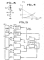
- Fig. 1-a represents the voltage VI across the diode when it is reverse biased (TV standby or standby period) and VD when it is forward biased (TE operation or transmission period).
- Fig. 1-b relates to the current passing through the diode, I I and ID respectively.
- Fig. 1-c shows the equalization of the electrical power in reverse PE and in direct PE D and FIG. 1-d the unchanged TJ temperature of the junction.
- the optical power PO transmitted is illustrated in FIG. 1-e; it is zero during each TV standby period due to the blocking of the emission by reverse polarization; it immediately reaches the desired value from the instant to transition to the operating state because the temperature of the junction was preserved during the previous TV phase.
- the PO value corresponds to the average power value.
- Fig. 2 shows an embodiment of an LED diode device according to the invention.
- the device represented in the form of an electrical circuit comprises the LED itself, a modulation input EM, a control input EC, two transistors QI and Q2, a capacitor C and the resistors R1, R2, RE and RC.
- the LED diode is forward biased by the current source constituted by the pnp transistor Ql, the resistors RE, R1, R2 and a direct voltage VC of polarity suitable for. mounting terminals.
- This voltage is obtained with the two continuous potentials Vccl and Vcc2, positive in the case considered, and applied on the side RI and R2 respectively.
- the RI-R2 branch polarizes the base of the transistor Q1 and determines the average current Io in the LED that charges the collector.
- the modulation is applied to the input EM and transmitted to the base of Q1 through the capacitor C to vary the polarization and correlatively the current through the transistor and the diode so as to modulate the emission of photons.
- Reverse polarization is achieved by a switch which has the role of connecting the diode to the terminals of the DC power supply Vccl.
- the switch circuit consists of transistor Q2 and resistors RC and RB.
- a positive voltage is applied to the input EC which causes the saturation conduction of the transistor Q2 and amounts to considering the resistance RC connected on this side of the ground as shown in FIG. 3.
- the resistors RB and RC are used to limit the currents.
- the LED diode is then reverse biased by the voltage Vccl.
- Fig. 4 represents the voltage-current characteristic of the LED diode in reverse as well as the load line relating to the RC resistance.
- the diode being reverse biased there is no light emission.
- the control voltage applied to the input EC drops to OV or to a slightly negative value to block the transistor Q2 and the LED diode circuit is reformed again through the transistor Ql .
- the LED diode is polarized by the current source Ql, R1, R2, RE and the value of the direct current is given by: (V BE ) Q1 being the voltage between base and transmitter of Ql.
- the voltage VD across the diode depends little on the current ID, and is generally close to 2V.
- the electrical power dissipated PE2 is equal to ID.VD.
- Vccl and RC are chosen to substantially equalize the values of dissipated power PE1 and PE2, the temperature of the junction will practically not change at the time of the passage from standby (Reverse polarized LED; no light emission) in operating state (direct polarized LED; light emission) and the assembly will not show any thermal time constant.
- the fact that the non-operational diodes at a given instant are not emissive results in the reception of only one light signal at a time, that of the LED diode of the operational transmitter, and avoids deterioration of the signal-to-noise ratio in the ratio which becomes ⁇ n for n identical transmitters.
- Fig. 5 shows an example of such use.
- the transmission system comprises n channels, each with a LED diode transmitter EDj, an optical receiver ROj and a decision logic LDj.
- the decision circuits LD1 to LDn are controlled from a central unit which is not shown, if only to manage the transmission of messages over time.
- the optical interconnections can be made with an optical coupler CO, for example a mixing rod, to which the transmitters and receivers are connected by optical fibers.
Landscapes
- Optical Communication System (AREA)
Applications Claiming Priority (2)
| Application Number | Priority Date | Filing Date | Title |
|---|---|---|---|
| FR8220965A FR2537782A1 (fr) | 1982-12-14 | 1982-12-14 | Dispositif a diode emettrice de lumiere amenage pour supprimer les effets de constante de temps thermique |
| FR8220965 | 1982-12-14 |
Publications (3)
| Publication Number | Publication Date |
|---|---|
| EP0112227A2 true EP0112227A2 (de) | 1984-06-27 |
| EP0112227A3 EP0112227A3 (en) | 1984-07-25 |
| EP0112227B1 EP0112227B1 (de) | 1987-02-11 |
Family
ID=9280091
Family Applications (1)
| Application Number | Title | Priority Date | Filing Date |
|---|---|---|---|
| EP83402323A Expired EP0112227B1 (de) | 1982-12-14 | 1983-12-02 | Einrichtung zum Unterdrücken von Auswirkungen der thermischen Zeitkonstanten bei einer Anordnung mit lichtemittierender Diode |
Country Status (4)
| Country | Link |
|---|---|
| US (1) | US4633525A (de) |
| EP (1) | EP0112227B1 (de) |
| DE (1) | DE3369811D1 (de) |
| FR (1) | FR2537782A1 (de) |
Families Citing this family (7)
| Publication number | Priority date | Publication date | Assignee | Title |
|---|---|---|---|---|
| US4752693A (en) * | 1983-03-31 | 1988-06-21 | Tokyo Shibaura Denki Kabushiki Kaisha | Circuit with a photo coupler |
| DE3714503C2 (de) * | 1987-04-30 | 1995-07-27 | Lambda Physik Forschung | Steuerschaltung für einen gepulsten Gas-Laser und Verfahren zum Initialisieren der Steuerschaltung |
| US4924473A (en) * | 1989-03-28 | 1990-05-08 | Raynet Corporation | Laser diode protection circuit |
| US5073838A (en) * | 1989-12-04 | 1991-12-17 | Ncr Corporation | Method and apparatus for preventing damage to a temperature-sensitive semiconductor device |
| WO2006092040A1 (en) * | 2005-03-03 | 2006-09-08 | Tir Systems Ltd. | Method and apparatus for controlling thermal stress in lighting devices |
| US7646988B2 (en) * | 2006-08-04 | 2010-01-12 | Finisar Corporation | Linear amplifier for use with laser driver signal |
| US7734184B2 (en) * | 2006-08-04 | 2010-06-08 | Finisar Corporation | Optical transceiver module having an active linear optoelectronic device |
Family Cites Families (9)
| Publication number | Priority date | Publication date | Assignee | Title |
|---|---|---|---|---|
| US3947753A (en) * | 1972-05-06 | 1976-03-30 | Canon Kabushiki Kaisha | Voltage regulator including an LED to provide a reference voltage |
| US3755679A (en) * | 1972-07-10 | 1973-08-28 | Monsanto Co | Constant photon energy source |
| US3946335A (en) * | 1975-02-18 | 1976-03-23 | Bell Telephone Laboratories, Incorporated | Stabilization circuit for radiation emitting diodes |
| US4243952A (en) * | 1978-10-30 | 1981-01-06 | Rca Corporation | Temperature compensated bias circuit for semiconductor lasers |
| US4359773A (en) * | 1980-07-07 | 1982-11-16 | Bell Telephone Laboratories, Incorporated | Semiconductor lasers with selective driving circuit |
| JPS5739593A (en) * | 1980-08-22 | 1982-03-04 | Nec Corp | Driving circuit of semiconductor light emitting element |
| SE424022B (sv) * | 1980-10-21 | 1982-06-21 | Asea Ab | Fiberoptiskt metdon for spektralanalys |
| US4412331A (en) * | 1981-04-22 | 1983-10-25 | M/A-Com Dcc, Inc. | Feedback circuit for controlling the peak optical output power of an injection laser |
| JPS587941A (ja) * | 1981-07-08 | 1983-01-17 | Nec Corp | 半導体発光素子高速駆動回路 |
-
1982
- 1982-12-14 FR FR8220965A patent/FR2537782A1/fr active Granted
-
1983
- 1983-12-02 DE DE8383402323T patent/DE3369811D1/de not_active Expired
- 1983-12-02 EP EP83402323A patent/EP0112227B1/de not_active Expired
- 1983-12-12 US US06/560,115 patent/US4633525A/en not_active Expired - Fee Related
Also Published As
| Publication number | Publication date |
|---|---|
| EP0112227B1 (de) | 1987-02-11 |
| US4633525A (en) | 1986-12-30 |
| FR2537782B1 (de) | 1985-03-08 |
| EP0112227A3 (en) | 1984-07-25 |
| FR2537782A1 (fr) | 1984-06-15 |
| DE3369811D1 (en) | 1987-03-19 |
Similar Documents
| Publication | Publication Date | Title |
|---|---|---|
| EP0052536B1 (de) | Sendermodul-Ausgangsleistungsstabilisierungsanordnung für ein Lichtwellenleiter-Übertragungssystem | |
| EP0034957B1 (de) | Vorrichtung zur automatischen Regulierung der Ausgangsleistung eines Sendermoduls für ein Übertragungssystem mit optischen Fasern | |
| EP0584013B1 (de) | Vorverzerrungsschaltung und optische Halbleiterlichtquelle mit solcher Schaltung | |
| EP0112227B1 (de) | Einrichtung zum Unterdrücken von Auswirkungen der thermischen Zeitkonstanten bei einer Anordnung mit lichtemittierender Diode | |
| EP0231015B1 (de) | Kohärente photonische Fernmeldeeinrichtung | |
| WO2015022281A1 (fr) | Procede et dispositif pour la regulation de l'alimentation d'un convertisseur photovoltaique | |
| EP0586285B1 (de) | Optischer Sender-Empfänger für optische Datenübertragung und Schalteinrichtung | |
| EP3248305B1 (de) | Ethernet-switch für faseroptisches netzwerk | |
| FR2520174A1 (fr) | Systeme de transmission de signaux numeriques sur fibre optique | |
| EP0199332B1 (de) | Empfänger für optische Breitbandsignale | |
| EP0467764B1 (de) | Optisches Vermittlungssystem für Frequenzmultiplexsignale | |
| EP0506186B1 (de) | Videoverstärkervorrichtung | |
| EP0099956A1 (de) | Signalempfänger und seine Verwendung in einer Emfangsschaltung die den Stand der angeschlossenen Einrichtung angibt | |
| EP0632309B1 (de) | Optischer Impulsgenerator | |
| EP0388846B1 (de) | Laserspeisungs- und Steuereinrichtung für Lichtwellenleiterverbindung zwischen einem Teilnehmer und einer Fernmeldevermittlungsanlage | |
| EP1455451B1 (de) | Vorrichtung zur optischen Signalverarbeitung | |
| EP1102148A1 (de) | Niedrigtemperaturkorrigierte Spannungsgeneratoreinrichtung | |
| EP1966888B1 (de) | Hochleistungsgenerator für elektrische impulse | |
| EP1236273B1 (de) | Hochspannungshybridschaltung | |
| FR2521372A1 (fr) | Emetteur pour systeme de transmission sur fibre optique | |
| WO2023170026A1 (fr) | Systeme de modulation configure pour controler la modulation d'un signal | |
| FR2566205A1 (fr) | Procede de controle d'un dispositif attenuateur/amplificateur a commande automatique de gain et recepteur optique | |
| FR2524741A1 (fr) | Dispositif de restitution d'informations transmises sur une fibre optique et recepteur comportant un tel dispositif | |
| FR2582887A1 (fr) | Emetteur optique a diode emettant des radiations. | |
| FR2648925A1 (fr) | Dispositif de regulation pour circuit d'alimentation stabilisee |
Legal Events
| Date | Code | Title | Description |
|---|---|---|---|
| PUAI | Public reference made under article 153(3) epc to a published international application that has entered the european phase |
Free format text: ORIGINAL CODE: 0009012 |
|
| PUAL | Search report despatched |
Free format text: ORIGINAL CODE: 0009013 |
|
| AK | Designated contracting states |
Designated state(s): BE CH DE GB IT LI SE |
|
| AK | Designated contracting states |
Designated state(s): BE CH DE GB IT LI SE |
|
| 17P | Request for examination filed |
Effective date: 19841215 |
|
| 17Q | First examination report despatched |
Effective date: 19860527 |
|
| RBV | Designated contracting states (corrected) |
Designated state(s): BE CH DE GB LI |
|
| GRAA | (expected) grant |
Free format text: ORIGINAL CODE: 0009210 |
|
| AK | Designated contracting states |
Kind code of ref document: B1 Designated state(s): BE CH DE GB LI |
|
| REF | Corresponds to: |
Ref document number: 3369811 Country of ref document: DE Date of ref document: 19870319 |
|
| PLBE | No opposition filed within time limit |
Free format text: ORIGINAL CODE: 0009261 |
|
| STAA | Information on the status of an ep patent application or granted ep patent |
Free format text: STATUS: NO OPPOSITION FILED WITHIN TIME LIMIT |
|
| 26N | No opposition filed | ||
| PGFP | Annual fee paid to national office [announced via postgrant information from national office to epo] |
Ref country code: CH Payment date: 19941118 Year of fee payment: 12 |
|
| PGFP | Annual fee paid to national office [announced via postgrant information from national office to epo] |
Ref country code: BE Payment date: 19941212 Year of fee payment: 12 |
|
| PGFP | Annual fee paid to national office [announced via postgrant information from national office to epo] |
Ref country code: DE Payment date: 19951120 Year of fee payment: 13 |
|
| PGFP | Annual fee paid to national office [announced via postgrant information from national office to epo] |
Ref country code: GB Payment date: 19951121 Year of fee payment: 13 |
|
| PG25 | Lapsed in a contracting state [announced via postgrant information from national office to epo] |
Ref country code: LI Effective date: 19951231 Ref country code: CH Effective date: 19951231 Ref country code: BE Effective date: 19951231 |
|
| BERE | Be: lapsed |
Owner name: THOMSON-CSF Effective date: 19951231 |
|
| REG | Reference to a national code |
Ref country code: CH Ref legal event code: PL |
|
| PG25 | Lapsed in a contracting state [announced via postgrant information from national office to epo] |
Ref country code: GB Effective date: 19961202 |
|
| GBPC | Gb: european patent ceased through non-payment of renewal fee |
Effective date: 19961202 |
|
| PG25 | Lapsed in a contracting state [announced via postgrant information from national office to epo] |
Ref country code: DE Effective date: 19970902 |