EP0112731A2 - Schnittstellenschaltung für eine Teilnehmerleitung - Google Patents
Schnittstellenschaltung für eine Teilnehmerleitung Download PDFInfo
- Publication number
- EP0112731A2 EP0112731A2 EP83307997A EP83307997A EP0112731A2 EP 0112731 A2 EP0112731 A2 EP 0112731A2 EP 83307997 A EP83307997 A EP 83307997A EP 83307997 A EP83307997 A EP 83307997A EP 0112731 A2 EP0112731 A2 EP 0112731A2
- Authority
- EP
- European Patent Office
- Prior art keywords
- coupled
- circuit
- output
- feedback
- subscriber line
- Prior art date
- Legal status (The legal status is an assumption and is not a legal conclusion. Google has not performed a legal analysis and makes no representation as to the accuracy of the status listed.)
- Granted
Links
- 230000004044 response Effects 0.000 claims description 12
- 230000001419 dependent effect Effects 0.000 claims description 3
- 230000015556 catabolic process Effects 0.000 claims 1
- 230000003111 delayed effect Effects 0.000 claims 1
- 230000000694 effects Effects 0.000 abstract description 2
- 239000003990 capacitor Substances 0.000 description 12
- 230000005540 biological transmission Effects 0.000 description 5
- 238000010586 diagram Methods 0.000 description 5
- 230000008901 benefit Effects 0.000 description 4
- 238000006243 chemical reaction Methods 0.000 description 4
- 230000002194 synthesizing effect Effects 0.000 description 4
- 238000001514 detection method Methods 0.000 description 2
- 230000010354 integration Effects 0.000 description 1
- 238000004519 manufacturing process Methods 0.000 description 1
- 238000012986 modification Methods 0.000 description 1
- 230000004048 modification Effects 0.000 description 1
- 231100000989 no adverse effect Toxicity 0.000 description 1
- 230000009467 reduction Effects 0.000 description 1
- 238000001228 spectrum Methods 0.000 description 1
Images


Classifications
-
- H—ELECTRICITY
- H04—ELECTRIC COMMUNICATION TECHNIQUE
- H04M—TELEPHONIC COMMUNICATION
- H04M3/00—Automatic or semi-automatic exchanges
- H04M3/005—Interface circuits for subscriber lines
-
- H—ELECTRICITY
- H04—ELECTRIC COMMUNICATION TECHNIQUE
- H04M—TELEPHONIC COMMUNICATION
- H04M19/00—Current supply arrangements for telephone systems
- H04M19/001—Current supply source at the exchanger providing current to substations
- H04M19/005—Feeding arrangements without the use of line transformers
Definitions
- the present invention relates to a telephone subscriber line interface circuit.
- the subscriber line interface circuit In digital telephone switching systems the subscriber line interface circuit is required to meet the various functions known as BORSHT which is an acronym of Batery feed, Over-voltage protection, Ringing current supply, Supervisory of line status, Hybrid circuit (two-wire to four-wire conversion) and Test of subscriber lines. Although many attempts have hitherto been made to implement these functions in integrated circuits for purposes of achieving compactness, improving reliability and reducing power dissipation, the proposed subscriber line interface circuits are not satisfactory in a number of aspects.
- United States Patent No. 4,387,273 granted to Ramon C. W. Chea, Jr. discloses a subscriber line interface circuit with an impedance synthesizer.
- the impedance synthesizer includes two resistors having their first ends coupled respectively to the subscriber line terminals and two voltage amplifiers which are connected to the opposite ends of the resistors, respectively.
- the voltage amplifiers are driven by a differential line voltage between the line terminals which is supplied through a circuit having a predetermined transfer function.
- the transfer function is set equal to a constant value k which is implemented by an inverting amplifier. If the gain of each voltage amplifier is unity, the impedance Z between the subscriber line terminals is represented by: where, R is the values of the aforesaid resistors.
- Equation 2 must be computed to determine the transfer function K, it is impossible to establish a one-to-one correspondence between the desired impedance and transfer function. However, from the circuit design standpoint it is required that the transfer function be an integral multiple of the desired impedance.
- a Transformerless hybrid circuit for circuit integration is described in Articles "Design and Performance of Subscriber line Interface Module for Digital Switching System", ISSCC 1980, by Keiichi Yasuda et al. and "A High-Voltage IC for a Transformerless Trunk and Subscriber Line Interface", IEEE Journal of Solid-State Circuits, Vol. SC-16, No.4, August 1981, Denis W. Aull et al.
- the hybrid circuits discussed in these publications include a crosstalk canceller which is designed so that it has no adverse effect on the transmission characteristic of the path from the input terminal of the four-wire circuit to the subscriber line and requires at least three impedance networks for synthesizing a terminal impedance Z T , a transmission impedance Z s and a balancing impedance Z B is used to balance against the load impedance Z L .
- a crosstalk canceller which is designed so that it has no adverse effect on the transmission characteristic of the path from the input terminal of the four-wire circuit to the subscriber line and requires at least three impedance networks for synthesizing a terminal impedance Z T , a transmission impedance Z s and a balancing impedance Z B is used to balance against the load impedance Z L .
- the impedance Z B is balanced against the load impedance, distortion can occur in the transmission characteristic of the path from the input line of four-wire circuit to the two-wire subscriber line if the terminal impedance
- a primary object of the present invention is to provide a subscriber line interface circuit which relaxes the precision requirements imposed on each stage of analog computation involved in synthesizing a desired impedance value by the provision of a first feedback loop which feeds back a signal havng the same voltage level as the input signal and second and third feedback loops each having a transfer function required to synthesize the desired impedance over a predetermined frequency range, whereby the high precision requirement is only required of the first feedback loop, reducing the number of high precision circuit components.
- a subscriber line interface circuit of the present invention comprises differential amplifier means coupled through line terminals to a two-wire subscriber line for detecting a voltage difference developed across the line terminals.
- First and second resistance means of equal resistance values each having first and second opposite ends.are connected at their first ends to the line terminals, respectively.
- Driver means is coupled to the second ends of the first and second resistance means for driving a load coupled to the distant end of the subscriber line.
- First, second and third feedback means are provided.
- the first feedback means is coupled from the output of the differential amplifier means to the input of the driver means for changing the impedance characteristics of the first and second resistance means so that a high impedance is synthesized across each of the first and second resistance means.
- the second and third feedback means are also coupled from the output of the differential amplifier means to the input of the driver means, each of the second and third feedback means having a different passband frequency characteristic for reducing the synthesized impedances to a predetermined value.
- a second object of the present invention is to provide a subscriber line interface circuit which includes a two-wire to four-wire converter having two impedance networks which dissipate less power than the prior art networks.
- a third object of the present invention is to provide a subscriber line interface circuit including a two-wire to four-wire converter having a flat frequency response characteristic from the input terminal of a four-wire circuit to the two-wire subscriber line.
- a fourth object of the present invention is to provide a subscriber line interface circuit in which the battery feeding circuit has a variable response time as a function of the amplitude of the input signal so that it presents a fast response characteristic to dial pulses.
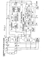
- a tip line of a two-wire subscriber loop is connected to a tip terminal T and a ring line of the loop connected to a ring terminal R, the loop having a load impedance Z L at the distant end of the loop in subscriber premises.
- a differential amplifier 1 whose output terminals are coupled through a first feedback loop fl to an input of a tip driver 2 and an input of a ring driver 3.
- the output terminals of the differential amplifier 1 are further coupled through a second feedback loop f 2 comprising an AC feedback circuit 4 and further through a third feedback loop f 3 including a DC feedback circuit 5.
- the AC feedback circuit 4 comprises a balance-unbalance converter 41, a hybrid circuit 42 and a voltage-to-current converter 43 which converts the output voltage of the hybrid circuit 42 to currents which are supplied to the tip driver 2 and ring driver 3, respectively.
- DC decoupling capacitors C are provided in the input and output circuits of the balance-unbalance converter 41.
- the balance-unbalance converter 41 provides conversion of the balanced output of the differential amplifier 1 to a signal unbalanced with respect to ground. While the capacitors C are provided both on the input and output circuits of the converter 41, the latter could equally as well operate if the capacitances are provided only in the input or output circuit thereof.
- the hybrid circuit 42 comprises a phase compensator 421 which introduces a predetermined amount of phase delay to a signal applied to an input terminal Rx of a four-wire circuit which is coupled to the telephone switching system.
- phase compensator 421 is weighted and summed in a summing circuit 422 with the output of the balance-unbalance converter 41 such that undesired components resulting from the circuit unbalance are canceled, the summed output being delivered to an output terminal Tx of the four-wire circuit.
- Impedance networks 424 and 425 are provided having impedances Z x and Zyr respectively.
- the summed output from circuit 422 is multiplied by a factor Z x at 424 and a unity-gain inverting amplifier 423 performs unity-gain inversion of an input signal at the four-wire input terminal Rx to be multiplied by a factor Zy at 425 which is combined with the signal multiplied by Z x in an operational amplifier 426 whose output is fed back to the negative going input thereof via a resistance R F at 427.
- the DC feedback circuit 5 includes a low-pass filter 51 which is coupled to one output of the differential amplifier 1.
- the low-pass filter 51 has a large time constant value when the input signal thereto has a small amplitude and a small time constant value when the input signal has a large amplitude.
- a voltage-to-current converter 52 is coupled to the output of the low-pass filter 51 to generate a current which is a function of the difference between the input voltage and a reference voltage Vref.
- Current mirror circuits 53 and 54 supply currents of equal value to the output current of the converter 52 to the tip driver 2 and the ring driver 3.
- the outputs of the tip and ring drivers 2 and 3 are connected via battery feed resistances R B at 8 and 9 to the tip and ring terminals T and R, respectively.
- a dial pulse detector 6 is connected across the resistors 8 and 9 to detect voltage changes thereacross to detect dialed pulses.
- Fig. 2 illustrates an equivalent circuit of the embodiment of Fig. 1.
- a voltage v 0 developed across the line terminals T and R is applied to the differential amplifier 1 and passes through first, second and third feedback loops f 1 , f 2 and f 3 whose outputs are combined in an adder AD1 and the combined output appears across the resistance R B .
- the first feedback loop f l feeds the output of the differential amplifier 1 via an operational amplifier OP1 to an adder AD1.
- the second feedback loop f 2 includes the capacitance C which passes the higher frequency components to the differential amplifier 41 whose output is coupled via an operational amplifier OP3 to an adder AD2 and through an operational amplifier OP4 to an adder AD3 and an operational amplifier OP5 to the adder ADl.
- the third feedback loop f 3 comprises the low-pass filter 51 and an operational amplifier OP2 whose output is coupled to the adder AD1.
- An input signal to the four-wire input terminal Rx is coupled by way of operational amplifiers 423 and OP7 to the adder AD3 where it is summed with the output of adder AD2 after passing through an operational amplifier OP4, the output of adder AD3 being coupled by an operational amplifier OP5 to the adder AD1 and through resistance R B , differential amplfier 1, capacitor C, differential amplfier 41 and operational amplifier OP3 to adder AD2, completing a loop.
- the signal applied to the input terminal Rx is also coupled by an operational amplifier OP6 to the adder AD2 where it cancels the four-wire input component of the second feedback loop f 2 to allow the two-wire signal to be exclusively delivered to the four-wire output terminal Tx.
- the operational amplifier OP6 is provided with a phase adjustment function which provides a phase delay to establish a phase match in the adder AD1.
- Battery feed resistances R B at 8 and 9 are synthesized by taking into account the total characteristic of the circuit from points S 0 , S1 to points S 2 , S 3' while at the same time making the voltage difference across points S2 and S3 satisfy the following equations: which can be rearranged as: where, v 0 is the line voltage across points S 0 and S 1 , V BB is the reference supply voltage, and k 0 is the ratio of resistance R B to synthesized equivalent resistance R FD .
- the line voltage v 0 which is expressed by the second term of Equation (1.2), is synthesized by the first feedback loop by setting the voltage gains of the differential amplifier 1 and operational amplifier OP1 to -1/2 and -2, respectively. This equalizes the voltages developed across resistances R B and no current thus flows therethrough. As a result, the first feedback loop has the effect of increasing the impedance values of the resistances R B .
- the voltage difference between points S 2 and S 3 is given by -(1/4)V BB - (1/4)v 0 .
- the center voltage of the two-wire circuit is given by (1/2)V BB and therefore application of a reference voltage (1/4)VBB to the amplifier OP2 results in a voltage -(1/4)V BB at the output thereof.
- the AC feedback loop included in the second feedback loop comprises a two-wire to four-wire converter.
- the difference signal which is detected by the differential amplifier 1 and multiplied by a factor -1/2, is passed through capacitance C so that the DC component of the signal is removed, converted to an unbalanced signal with a unity gain by differential amplifier 41, and amplified by operational amplifier OP3 having a gain -2, whereby the voltage difference v 0 across points S 0 and S 1 appears at the output of amplifier OP3.
- Voltage at the four-wire input terminal R X through an inverting unity gain amplifier OP6 is subtracted from the output voltage of amplifier OP3 in the adder AD2 whose output is delivered to the output line of the four-wire circuit.
- the signal from the four-wire input terminal Rx is further passed through an inverting unit gain amplifier 423 to operational amplifier OP7 where it is multiplied by a factor -R F/ Z Y and applied to the adder AD3.
- the output voltage of adder AD2 is multiplied by a factor -R F /Z X by amplifier OP4 and fed to adder AD3.
- the output of adder AD3 is applied to an amplifier OP5 which corresponds to the voltage-to-current converter 43 of Fig. 1 where it is multiplied by a factor 2 and applied to adder ADl.
- the circuit from the four-wire input terminal Rx to the two-wire circuit has a transfer function "1" which is equal to the transfer function of the circuit from the two-wire circuit to the four-wire output terminal Tx.
- FIG. 3 to 5 Illustrated in Figs. 3 to 5 is a practical embodiment of the circuit of Fig. 1 having the operating characteristics just described with reference to Fig. 2.
- the tip driver 2 comprises an operational amplifier 21 and resistors R21 to R23 and the ring driver 3 comprises an operational amplifier 31 and resistors R31 to R33.
- the tip driver 2 and ring driver 3 will have a gain of -2 with which the voltages at points S 4 and S 5 are multiplied. Therefore, the voltages at points S and S 1 are rendered equal to the voltages at points S2 and S 3 .
- the output of the operational amplifier 21 is coupled by a feedback circuit including resistors R21, R22 to its inverting input and likewise the output of the operational amplifier 31 is coupled by a feedback circuit including resistors R31, R32 to its inverting input.
- the noninverting inputs of both operational amplifiers 21, 31 are biased at a reference voltage Vrefl which is set equal to (1/2)VBB derived from a voltage source at V BB by a resistor network and an operational amplifier 20.
- the dial pulse detector 6 comprises an operational amplifier 61, a discriminator 62 and resistors R61 and R62 and connected in circuit with resistors RDl to RD4 to opposite terminals of resistances R B to detect the voltages developed thereacross and hence a loop current.
- the discriminator 62 compares the loop current value with a threshold and reconstructs the received dial pulses by generating sharply defined pulses.
- Fig. 4 illustrates the detail of the AC feedback circuit 4 of Fig. 1.
- the balance-to-unbalance converter 41 is formed by an operational amplifier 411 and resistors R411 to R414 and arranged to detect the differential signal of the two-wire subscriber line.
- R412/R411 1
- the phase compensator 421 is formed by a resistor R711 and a capacitor C711 which are connected in a low-pass filter configuration.
- This phase compensator provides a phase matching between the signal from the four-wire input terminal Rx with a signal which is fed back thereto through the impedance network 425 and through the output loop of the AC feedback circuit 4.
- R723/(R711 + R722) 1, the signal from the input terminal Rx is multiplied by the operational amplifier 721 with a gain -1.
- the impedance network 424 can be formed by a series circuit of a 90-killohm resistor and a 0.0216-microfarad capacitor.
- the amplifier 423 comprises an input resistor R731 and a feedback resistor R732 of like values and an operational amplifier 731 and coupled to the input terminal Rx so that it multiplies the signal therefrom with a gain of -1.
- the operational amplifier 426 has a resistance R F at 427 which is combined with the impedances Z x and Zy of the networks 424 and 425 so that the amplifier 426 is given voltage gains of -R F /Z X and -R F /Z Y . If the following relation holds, The voltage gains of the amplifier 426 become -R B /Z T and - R B / Z B , respectively.
- the voltage-to-current converter 43 which converts the output voltage of hybrid circuit 42 to a corresponding current, comprises a transistor Q431 having a base coupled to the output of the hybrid circuit 42 and a transistor Q432 having a base coupled to ground, the emitters of these transistors being coupled by a resistor R431.
- the emitters and collectors of the transistors Q431 and Q432 are coupled to constant current sources formed by transistors Q433 through Q440, resistors R432 and R433 and a Zener diode Z431 which are connected so that a constant current is generated at each of the collectors of transistors Q433 to Q436.
- the output current I 43 which flows through the collectors of transistors Q431, Q432 and through the resistors R22 and R32 of tip and ring drivers 2, 3 (Fig. 3), is given by where v 1 is the voltage impressed on the base of transistor Q431.
- the voltage output of the hybrid circuit 42 is applied to the tip driver 2 and ring driver 3 in opposite polarities to each other, so that the voltage gain 2 of amplifier OP5, Fig. 2, is obtained.
- an overall characteristic of -2R F/ Z X which is attributed to the second feedback loop, is obtained.
- the low-pass filter 51 comprises a resistor R512 which is connected in series with a pair of oppositely coupled Zener diodes Z511 and Z512 with the series circuit being in shunt with a resistor R511 to form a resistor-diode network one end of which is coupled to the output of differential amplifier 1 and the other end of which is coupled to a capacitor C511.
- the resistor R511 has a much larger value than that of resistor R512.
- the Zener diodes Z511, Z512 become conductive and in this case the resistor R512 and capacitor C511 form a low-pass filter having a small time constant value, thereby synthesizing small-valued phantom inductances.
- the voltage-to-current converter 52 is formed by a resistor R521, transistor Q521 and an operational amplifier 521 having a noninverting input coupled to be responsive to the output of the low-pass filter 51.
- the output current I 5 of this converter 52 flows through the current mirror circuits 53, 54 to the resistors R22, R32 of the tip and ring drivers 2, 3 (see Fig. 3).
- the first feedback loop synthesizes high impedances by changing the impedance characteristics of the resistors R B to high values.
- the second feedback loop has a transfer function -2RF/zX which acts in a way to reduce the impedance realized by the first feedback loop between the line terminals T and R of the two-wire subcriber line to a desired value.
- This impedance reduction occurs exclusively at frequencies higher than a frequency value determined by the high-pass frequency characteristic of the DC decoupling capacitors of the second feedback loop.
- the third feedback loop acts in a way to reduce the high impedances realized by the first feedback loop to lower impedance values desired between the terminal T and ground and between the terminal R and voltage source at V BB in a frequency range determined by the inherent low-pass frequency characteristic of the third feedback loop.
- the second and third feedback loops differ in operating frequency range, both of these loops can be treated as a loop having an equal function having regard to their impedance reducing characteristis. Therefore, the first and second feedback loops are taken up in the following description.
- the input impedance Z looking into the subscriber line from the line terminals T, R is: By appropriately determining the ratio of R F of the impedance network 424 to Z X of the feedback resistor 427 (Fig. 4), a desired impedance value can be realized between the terminals T and R.
- the absolute value of the ⁇ G 2 -dependent deviation of impedance Z equals the absolute value of the deviation of transfer function G 2 .
- the present invention thus requires high precision circuit elements to be provided only in the first feedback loop. Only the operational amplifier 1 and those used in the tip driver 2 and ring driver 3 are the ones that are required to meet the wide bandwidth requirement. Use of high precision type resistors is also limited to those employed in the first feedback loop. The other operational amplifiers and their feedback resistors, the input impedance and resistor, and the summing resistors are only required to meet the precision and bandwidth requirements imposed between the terminals T and R. Hence, the second and third feedback loops need not be constructed of high precision components. This is advantageous both in circuit design and manufacture. While mention has been made of an impedance synthesizer of which the impedance is balanced with respect ground, it is obvious to provide an impedance synthesizer having an unbalanced impedance with respect to ground.
- V F the feedback voltage developed between the outputs of the tip and ring drivers 2, 3 is given by Equation (4.1) where V 2w is the line voltage to be transmitted to the two-wire subscriber line and V Rx represent the voltage developed at the terminal Rx.
- V 2w is given by where, Z L is the load impedance of the two-wire subscriber line.
- Another advantage resides in the fact that, since the impedance values of the networks 424 and 425 can have desired values, the invention requires no reactance components for feeding currents to the two-wire subscriber line. Simple resistance elements such as current feeding resistors R B are sufficient for this purpose. From the practical' standpoint, it is not necessary to treat such resistance elements as impedance networks.
- the transfer function H LFS of the low-pass filter 51 for small amplitude signals is given by Equation (5.1), where, C 511 and R 511 are the capacitance and resistance values of the capacitor C511 and resistor R511, respectively.
- the transfer function H LFL for large amplitude input signals is given by Equation (5.2), where, R 512 is the resistance value of resistor R512.
- the subscriber line interface circuit of the present invention presents a high impedance to small amplitude signals such as speech signals and a low impedance to large amplitude signals such as dial pulses.
- the response time of the line interface circuit is 100 milliseconds to speech signals and 0.1 milliseconds to dial pulses. Dial pulses can thus be sharply discriminated.
Landscapes
- Engineering & Computer Science (AREA)
- Signal Processing (AREA)
- Power Engineering (AREA)
- Interface Circuits In Exchanges (AREA)
Applications Claiming Priority (10)
| Application Number | Priority Date | Filing Date | Title |
|---|---|---|---|
| JP22907082A JPS59122110A (ja) | 1982-12-28 | 1982-12-28 | インピ−ダンス合成回路 |
| JP229070/82 | 1982-12-28 | ||
| JP22999082A JPS59123307A (ja) | 1982-12-29 | 1982-12-29 | インピ−ダンス合成回路 |
| JP229990/82 | 1982-12-29 | ||
| JP58106206A JPS59231930A (ja) | 1983-06-14 | 1983-06-14 | 2線−4線変換回路 |
| JP106206/83 | 1983-06-14 | ||
| JP58159825A JPS6051359A (ja) | 1983-08-31 | 1983-08-31 | 加入者回路の給電回路 |
| JP159825/83 | 1983-08-31 | ||
| JP21556283A JPS60107118A (ja) | 1983-11-16 | 1983-11-16 | 電圧電流変換回路 |
| JP215562/83 | 1983-11-16 |
Publications (3)
| Publication Number | Publication Date |
|---|---|
| EP0112731A2 true EP0112731A2 (de) | 1984-07-04 |
| EP0112731A3 EP0112731A3 (en) | 1986-06-25 |
| EP0112731B1 EP0112731B1 (de) | 1988-11-09 |
Family
ID=27526264
Family Applications (1)
| Application Number | Title | Priority Date | Filing Date |
|---|---|---|---|
| EP83307997A Expired EP0112731B1 (de) | 1982-12-28 | 1983-12-29 | Schnittstellenschaltung für eine Teilnehmerleitung |
Country Status (5)
| Country | Link |
|---|---|
| US (1) | US4600811A (de) |
| EP (1) | EP0112731B1 (de) |
| AU (1) | AU563506B2 (de) |
| CA (1) | CA1206649A (de) |
| DE (1) | DE3378455D1 (de) |
Cited By (11)
| Publication number | Priority date | Publication date | Assignee | Title |
|---|---|---|---|---|
| EP0173387A1 (de) * | 1984-08-20 | 1986-03-05 | Koninklijke Philips Electronics N.V. | Optoelektrischer Signalumwandler |
| WO1987007104A1 (en) * | 1986-05-06 | 1987-11-19 | Telefonaktiebolaget Lm Ericsson | Apparatus in a telecommunication system for supplying power to a telephone set |
| EP0147230A3 (en) * | 1983-12-28 | 1988-04-20 | Nec Corporation | Subscriber line interface circuit having an impedance synthesizer |
| EP0215677A3 (en) * | 1985-09-20 | 1989-01-18 | Nec Corporation | Subscriber line interface circuit having means for combining dc and ac feedback signals |
| EP0221519A3 (de) * | 1985-11-06 | 1989-03-01 | AT&T Corp. | Weckanlegeschaltung |
| EP0212632A3 (en) * | 1985-08-20 | 1989-05-10 | Fujitsu Limited | Subscriber line interface circuit |
| FR2637142A1 (fr) * | 1988-09-28 | 1990-03-30 | Cit Alcatel | Dispositif de raccordement de ligne d'abonne |
| FR2642593A1 (fr) * | 1989-01-31 | 1990-08-03 | Cit Alcatel | Dispositif electronique de raccordement de ligne d'abonne |
| WO1993021723A1 (en) * | 1992-04-16 | 1993-10-28 | Northern Telecom Limited | Impedance synthesizer for a subscriber line interface circuit |
| EP0543161A3 (en) * | 1991-10-23 | 1993-12-08 | Sgs Thomson Microelectronics | Method and circuit device for measuring operation paramaters of an interface circuit and a telephone subscriber line connected thereto |
| EP0600175A1 (de) * | 1992-11-30 | 1994-06-08 | Motorola, Inc. | Teilnehmerleitungsschnittstellenschaltung zur Steuerung der Wechsel- und Gleichstromausgangsimpedanz |
Families Citing this family (25)
| Publication number | Priority date | Publication date | Assignee | Title |
|---|---|---|---|---|
| DE3428106A1 (de) * | 1984-07-30 | 1986-02-06 | Standard Elektrik Lorenz Ag, 7000 Stuttgart | Teilnehmeranschlussschaltung |
| AT384919B (de) * | 1984-10-05 | 1988-01-25 | Alcatel Austria Ag | Schaltungsanordnung fuer fernsprechnetze |
| JPS61154347A (ja) * | 1984-12-27 | 1986-07-14 | Fujitsu Ltd | 交換機の給電回路 |
| CA1231480A (en) * | 1985-03-15 | 1988-01-12 | John A. Barsellotti | Constant current line circuit |
| DE3513625A1 (de) * | 1985-04-16 | 1986-10-23 | Nixdorf Computer Ag, 4790 Paderborn | Schaltungsanordnung fuer die fernspeisung von teilnehmeranschluss-endgeraeten in fernmeldeanlagen |
| US4727574A (en) * | 1985-09-24 | 1988-02-23 | Northern Telecom Limited | Subscriber line interface circuit with improved d.c. balance |
| JP2645022B2 (ja) * | 1987-08-21 | 1997-08-25 | 株式会社東芝 | 加入者回路 |
| US5043655A (en) * | 1989-03-14 | 1991-08-27 | John Fluke Mfg. Co., Inc. | Current sensing buffer for digital signal line testing |
| US4922531A (en) * | 1989-04-19 | 1990-05-01 | Northern Telecom Limited | Line interface circuit |
| JP2780363B2 (ja) * | 1989-08-11 | 1998-07-30 | 富士通株式会社 | ハイブリッド回路 |
| US5251257A (en) * | 1990-09-12 | 1993-10-05 | Sharp Kabushiki Kaisha | 2-wire/3-wire converting apparatus |
| US5602912A (en) * | 1994-05-16 | 1997-02-11 | Silicon Systems, Inc. | Telephone hybrid circuit |
| JP2845181B2 (ja) * | 1995-09-22 | 1999-01-13 | 日本電気株式会社 | 加入者回路 |
| DE19636954B4 (de) * | 1996-09-11 | 2005-08-18 | Infineon Technologies Ag | Teilnehmerschaltung |
| US6115469A (en) * | 1998-08-25 | 2000-09-05 | Unitrode Corporation | Telephone line ring signal and DC power generator |
| US6760380B1 (en) * | 1998-12-07 | 2004-07-06 | Lynk Labs, Inc. | Data transmission apparatus and method |
| WO2001049012A1 (en) * | 1999-12-27 | 2001-07-05 | Nortel Networks Limited | Line interface circuit with two feedback loops to synthesise required impedance |
| DE10120070A1 (de) * | 2001-04-24 | 2002-11-07 | Siemens Ag | Vorrichtung und Verfahren zum Anpassen der Leitungseigenschaften bei hochbitratigen Datenübertragungen |
| DE102004014196A1 (de) * | 2004-03-23 | 2005-10-20 | Siemens Ag | Schaltungsanordnung und Verfahren zur Anpassung von Übertragungsstrecken |
| US20070291929A1 (en) * | 2006-06-15 | 2007-12-20 | Apfel Russell J | Methods and apparatus for performing subscriber line interface functions |
| US7970125B2 (en) * | 2006-06-15 | 2011-06-28 | Silicon Laboratories Inc. | Output stacking architecture for an amplifier |
| US7925005B2 (en) * | 2006-10-23 | 2011-04-12 | Silicon Laboratories, Inc. | Longitudinal balance calibration for a subscriber line interface circuit |
| US8249247B2 (en) * | 2006-12-27 | 2012-08-21 | Silicon Laboratories Inc. | Tracking voltage regulator for a subscriber line interface circuit |
| US8019077B2 (en) * | 2006-12-27 | 2011-09-13 | Silicon Laboratories Inc. | Methods and apparatus for low voltage control of a subscriber line interface circuit |
| CA3025346A1 (en) * | 2016-05-26 | 2017-11-30 | Leroy Thomas KUHN | Method and apparatus for separating and measuring multiphase immiscible fluid mixtures |
Family Cites Families (12)
| Publication number | Priority date | Publication date | Assignee | Title |
|---|---|---|---|---|
| ZA784547B (en) * | 1977-08-17 | 1979-08-29 | Post Office | Unbalanced/balanced converter circuits |
| US4292478A (en) * | 1979-05-25 | 1981-09-29 | Plessey Canada Limited | Interface circuits |
| US4375015A (en) * | 1979-06-04 | 1983-02-22 | Tellabs, Inc. | Improved electronic hybrid circuit |
| US4315107A (en) * | 1979-10-15 | 1982-02-09 | Bell Telephone Laboratories, Incorporated | Telephone range extender with gain |
| US4315106A (en) * | 1979-11-28 | 1982-02-09 | International Telephone And Telegraph Corporation | Apparatus for regulating current supplied to a telephone line signal of the type employed in digital telephone systems |
| US4359609A (en) * | 1980-06-20 | 1982-11-16 | Advanced Micro Devices, Inc. | Circuit with feedback for controlling the impedance thereof |
| US4387273A (en) * | 1980-08-25 | 1983-06-07 | International Telephone And Telegraph Corporation | Subscriber line interface circuit with impedance synthesizer |
| CA1154185A (en) * | 1981-01-23 | 1983-09-20 | Patrick R. Beirne | Subscriber line interface circuit |
| DE3104138A1 (de) * | 1981-02-06 | 1982-08-19 | TE KA DE Felten & Guilleaume Fernmeldeanlagen GmbH, 8500 Nürnberg | Teilnehmerschaltung |
| US4476350A (en) * | 1981-02-17 | 1984-10-09 | Bell Telephone Laboratories, Incorporated | Battery feed circuit |
| US4388500A (en) * | 1981-02-27 | 1983-06-14 | Wescom, Inc. | Electronic hybrid |
| US4514595A (en) * | 1982-06-10 | 1985-04-30 | Northern Telecom Limited | Active impedance line feed circuit |
-
1983
- 1983-12-27 US US06/565,975 patent/US4600811A/en not_active Expired - Lifetime
- 1983-12-29 CA CA000444391A patent/CA1206649A/en not_active Expired
- 1983-12-29 EP EP83307997A patent/EP0112731B1/de not_active Expired
- 1983-12-29 DE DE8383307997T patent/DE3378455D1/de not_active Expired
- 1983-12-29 AU AU22978/83A patent/AU563506B2/en not_active Ceased
Cited By (15)
| Publication number | Priority date | Publication date | Assignee | Title |
|---|---|---|---|---|
| EP0147230A3 (en) * | 1983-12-28 | 1988-04-20 | Nec Corporation | Subscriber line interface circuit having an impedance synthesizer |
| EP0173387A1 (de) * | 1984-08-20 | 1986-03-05 | Koninklijke Philips Electronics N.V. | Optoelektrischer Signalumwandler |
| EP0212632A3 (en) * | 1985-08-20 | 1989-05-10 | Fujitsu Limited | Subscriber line interface circuit |
| EP0215677A3 (en) * | 1985-09-20 | 1989-01-18 | Nec Corporation | Subscriber line interface circuit having means for combining dc and ac feedback signals |
| EP0221519A3 (de) * | 1985-11-06 | 1989-03-01 | AT&T Corp. | Weckanlegeschaltung |
| WO1987007104A1 (en) * | 1986-05-06 | 1987-11-19 | Telefonaktiebolaget Lm Ericsson | Apparatus in a telecommunication system for supplying power to a telephone set |
| FR2637142A1 (fr) * | 1988-09-28 | 1990-03-30 | Cit Alcatel | Dispositif de raccordement de ligne d'abonne |
| FR2642593A1 (fr) * | 1989-01-31 | 1990-08-03 | Cit Alcatel | Dispositif electronique de raccordement de ligne d'abonne |
| EP0381105A1 (de) * | 1989-01-31 | 1990-08-08 | Alcatel Cit | Elektronische Anschlusseinrichtung für eine Teilnehmerleitung |
| US5097503A (en) * | 1989-01-31 | 1992-03-17 | Alcatel Cit | Electronic subscriber line connection circuit |
| EP0543161A3 (en) * | 1991-10-23 | 1993-12-08 | Sgs Thomson Microelectronics | Method and circuit device for measuring operation paramaters of an interface circuit and a telephone subscriber line connected thereto |
| US5440612A (en) * | 1991-10-23 | 1995-08-08 | Sgs-Thomson Microelectronics S.R.L. | Method and device for measuring operation parameters of telephone subscriber lines and associated interface circuits |
| WO1993021723A1 (en) * | 1992-04-16 | 1993-10-28 | Northern Telecom Limited | Impedance synthesizer for a subscriber line interface circuit |
| US5258713A (en) * | 1992-04-16 | 1993-11-02 | Northern Telecom Limited | Impedance generator for a telephone line interface circuit |
| EP0600175A1 (de) * | 1992-11-30 | 1994-06-08 | Motorola, Inc. | Teilnehmerleitungsschnittstellenschaltung zur Steuerung der Wechsel- und Gleichstromausgangsimpedanz |
Also Published As
| Publication number | Publication date |
|---|---|
| EP0112731B1 (de) | 1988-11-09 |
| AU563506B2 (en) | 1987-07-09 |
| CA1206649A (en) | 1986-06-24 |
| DE3378455D1 (en) | 1988-12-15 |
| US4600811A (en) | 1986-07-15 |
| EP0112731A3 (en) | 1986-06-25 |
| AU2297883A (en) | 1984-07-05 |
Similar Documents
| Publication | Publication Date | Title |
|---|---|---|
| US4600811A (en) | Subscriber line interface circuit | |
| US4387273A (en) | Subscriber line interface circuit with impedance synthesizer | |
| US4899382A (en) | Telephone circuit using DC blocked transformer and negative impedance technique | |
| US4567331A (en) | Electronic hybrid having synthesized impedance circuitry | |
| US3982080A (en) | Automatic cable balancing network | |
| US4472608A (en) | Subscriber line interface circuit | |
| JPS6094593A (ja) | インターフエイス回路、音声データインターフエイス回路および音声データ信号を回路内でインターフエイスする方法 | |
| US4359609A (en) | Circuit with feedback for controlling the impedance thereof | |
| US4866767A (en) | Subscriber line interface circuit | |
| US5402485A (en) | Two-wire termination impedance generation circuit of subscriber circuit | |
| US3989902A (en) | Alternating current regulator for use with telephone type line | |
| EP0247118A1 (de) | Schnittstellenschaltung. | |
| US4281219A (en) | Telephone line circuit | |
| US3789155A (en) | Side-tone reducing circuit for a telephone subscribers instrument | |
| US4400588A (en) | Electronic voice network for a telephone subscriber's substation | |
| JPS6041909B2 (ja) | 電話機通話回路網 | |
| CA2035099C (en) | Method and configuration for forming a line termination of a telephone line | |
| EP0116767B1 (de) | Speiseschaltung für eine Fernsprechteilnehmerleitung | |
| CA1267738A (en) | Telephone set comprising a line voltage stabilizer having a dc supply point | |
| JPS59135961A (ja) | 電話機用送話信号抑制回路 | |
| US4031331A (en) | Telephone speech network | |
| JPH0834605B2 (ja) | 加入者回路 | |
| JPS5912638A (ja) | インピ−ダンス合成形ライン回路 | |
| US4622442A (en) | Electronic hybrid having synthesized impedance circuitry | |
| US3597550A (en) | Balanced telephone instrument circuit |
Legal Events
| Date | Code | Title | Description |
|---|---|---|---|
| PUAI | Public reference made under article 153(3) epc to a published international application that has entered the european phase |
Free format text: ORIGINAL CODE: 0009012 |
|
| 17P | Request for examination filed |
Effective date: 19840117 |
|
| AK | Designated contracting states |
Designated state(s): BE DE FR GB IT NL SE |
|
| PUAL | Search report despatched |
Free format text: ORIGINAL CODE: 0009013 |
|
| AK | Designated contracting states |
Kind code of ref document: A3 Designated state(s): BE DE FR GB IT NL SE |
|
| 17Q | First examination report despatched |
Effective date: 19870706 |
|
| GRAA | (expected) grant |
Free format text: ORIGINAL CODE: 0009210 |
|
| AK | Designated contracting states |
Kind code of ref document: B1 Designated state(s): BE DE FR GB IT NL SE |
|
| REF | Corresponds to: |
Ref document number: 3378455 Country of ref document: DE Date of ref document: 19881215 |
|
| ET | Fr: translation filed | ||
| ITF | It: translation for a ep patent filed | ||
| PLBE | No opposition filed within time limit |
Free format text: ORIGINAL CODE: 0009261 |
|
| STAA | Information on the status of an ep patent application or granted ep patent |
Free format text: STATUS: NO OPPOSITION FILED WITHIN TIME LIMIT |
|
| 26N | No opposition filed | ||
| ITTA | It: last paid annual fee | ||
| EAL | Se: european patent in force in sweden |
Ref document number: 83307997.3 |
|
| PGFP | Annual fee paid to national office [announced via postgrant information from national office to epo] |
Ref country code: BE Payment date: 20001128 Year of fee payment: 18 |
|
| PGFP | Annual fee paid to national office [announced via postgrant information from national office to epo] |
Ref country code: SE Payment date: 20001212 Year of fee payment: 18 Ref country code: FR Payment date: 20001212 Year of fee payment: 18 |
|
| PGFP | Annual fee paid to national office [announced via postgrant information from national office to epo] |
Ref country code: GB Payment date: 20001227 Year of fee payment: 18 |
|
| PGFP | Annual fee paid to national office [announced via postgrant information from national office to epo] |
Ref country code: DE Payment date: 20001228 Year of fee payment: 18 |
|
| PGFP | Annual fee paid to national office [announced via postgrant information from national office to epo] |
Ref country code: NL Payment date: 20001231 Year of fee payment: 18 |
|
| PG25 | Lapsed in a contracting state [announced via postgrant information from national office to epo] |
Ref country code: GB Free format text: LAPSE BECAUSE OF NON-PAYMENT OF DUE FEES Effective date: 20011229 |
|
| PG25 | Lapsed in a contracting state [announced via postgrant information from national office to epo] |
Ref country code: SE Free format text: LAPSE BECAUSE OF NON-PAYMENT OF DUE FEES Effective date: 20011230 |
|
| PG25 | Lapsed in a contracting state [announced via postgrant information from national office to epo] |
Ref country code: BE Free format text: LAPSE BECAUSE OF NON-PAYMENT OF DUE FEES Effective date: 20011231 |
|
| REG | Reference to a national code |
Ref country code: GB Ref legal event code: IF02 |
|
| BERE | Be: lapsed |
Owner name: NEC CORP. Effective date: 20011231 |
|
| PG25 | Lapsed in a contracting state [announced via postgrant information from national office to epo] |
Ref country code: NL Free format text: LAPSE BECAUSE OF NON-PAYMENT OF DUE FEES Effective date: 20020701 |
|
| PG25 | Lapsed in a contracting state [announced via postgrant information from national office to epo] |
Ref country code: DE Free format text: LAPSE BECAUSE OF NON-PAYMENT OF DUE FEES Effective date: 20020702 |
|
| EUG | Se: european patent has lapsed |
Ref document number: 83307997.3 |
|
| GBPC | Gb: european patent ceased through non-payment of renewal fee |
Effective date: 20011229 |
|
| PG25 | Lapsed in a contracting state [announced via postgrant information from national office to epo] |
Ref country code: FR Free format text: LAPSE BECAUSE OF NON-PAYMENT OF DUE FEES Effective date: 20020830 |
|
| NLV4 | Nl: lapsed or anulled due to non-payment of the annual fee |
Effective date: 20020701 |
|
| REG | Reference to a national code |
Ref country code: FR Ref legal event code: ST |