EP0112899B1 - Broche a borne portant une soudure - Google Patents
Broche a borne portant une soudure Download PDFInfo
- Publication number
- EP0112899B1 EP0112899B1 EP83902372A EP83902372A EP0112899B1 EP 0112899 B1 EP0112899 B1 EP 0112899B1 EP 83902372 A EP83902372 A EP 83902372A EP 83902372 A EP83902372 A EP 83902372A EP 0112899 B1 EP0112899 B1 EP 0112899B1
- Authority
- EP
- European Patent Office
- Prior art keywords
- body portion
- solder
- pin
- substrate
- finger
- Prior art date
- Legal status (The legal status is an assumption and is not a legal conclusion. Google has not performed a legal analysis and makes no representation as to the accuracy of the status listed.)
- Expired
Links
Images

Classifications
-
- H—ELECTRICITY
- H01—ELECTRIC ELEMENTS
- H01R—ELECTRICALLY-CONDUCTIVE CONNECTIONS; STRUCTURAL ASSOCIATIONS OF A PLURALITY OF MUTUALLY-INSULATED ELECTRICAL CONNECTING ELEMENTS; COUPLING DEVICES; CURRENT COLLECTORS
- H01R12/00—Structural associations of a plurality of mutually-insulated electrical connecting elements, specially adapted for printed circuits, e.g. printed circuit boards [PCB], flat or ribbon cables, or like generally planar structures, e.g. terminal strips, terminal blocks; Coupling devices specially adapted for printed circuits, flat or ribbon cables, or like generally planar structures; Terminals specially adapted for contact with, or insertion into, printed circuits, flat or ribbon cables, or like generally planar structures
- H01R12/50—Fixed connections
- H01R12/51—Fixed connections for rigid printed circuits or like structures
- H01R12/55—Fixed connections for rigid printed circuits or like structures characterised by the terminals
- H01R12/58—Fixed connections for rigid printed circuits or like structures characterised by the terminals terminals for insertion into holes
- H01R12/585—Terminals having a press fit or a compliant portion and a shank passing through a hole in the printed circuit board
-
- H—ELECTRICITY
- H05—ELECTRIC TECHNIQUES NOT OTHERWISE PROVIDED FOR
- H05K—PRINTED CIRCUITS; CASINGS OR CONSTRUCTIONAL DETAILS OF ELECTRIC APPARATUS; MANUFACTURE OF ASSEMBLAGES OF ELECTRICAL COMPONENTS
- H05K3/00—Apparatus or processes for manufacturing printed circuits
- H05K3/30—Assembling printed circuits with electric components, e.g. with resistors
- H05K3/32—Assembling printed circuits with electric components, e.g. with resistors electrically connecting electric components or wires to printed circuits
- H05K3/34—Assembling printed circuits with electric components, e.g. with resistors electrically connecting electric components or wires to printed circuits by soldering
- H05K3/3447—Lead-in-hole components
-
- H—ELECTRICITY
- H01—ELECTRIC ELEMENTS
- H01R—ELECTRICALLY-CONDUCTIVE CONNECTIONS; STRUCTURAL ASSOCIATIONS OF A PLURALITY OF MUTUALLY-INSULATED ELECTRICAL CONNECTING ELEMENTS; COUPLING DEVICES; CURRENT COLLECTORS
- H01R4/00—Electrically-conductive connections between two or more conductive members in direct contact, i.e. touching one another; Means for effecting or maintaining such contact; Electrically-conductive connections having two or more spaced connecting locations for conductors and using contact members penetrating insulation
- H01R4/02—Soldered or welded connections
-
- H—ELECTRICITY
- H05—ELECTRIC TECHNIQUES NOT OTHERWISE PROVIDED FOR
- H05K—PRINTED CIRCUITS; CASINGS OR CONSTRUCTIONAL DETAILS OF ELECTRIC APPARATUS; MANUFACTURE OF ASSEMBLAGES OF ELECTRICAL COMPONENTS
- H05K2201/00—Indexing scheme relating to printed circuits covered by H05K1/00
- H05K2201/10—Details of components or other objects attached to or integrated in a printed circuit board
- H05K2201/10227—Other objects, e.g. metallic pieces
- H05K2201/10295—Metallic connector elements partly mounted in a hole of the PCB
- H05K2201/10303—Pin-in-hole mounted pins
-
- H—ELECTRICITY
- H05—ELECTRIC TECHNIQUES NOT OTHERWISE PROVIDED FOR
- H05K—PRINTED CIRCUITS; CASINGS OR CONSTRUCTIONAL DETAILS OF ELECTRIC APPARATUS; MANUFACTURE OF ASSEMBLAGES OF ELECTRICAL COMPONENTS
- H05K2201/00—Indexing scheme relating to printed circuits covered by H05K1/00
- H05K2201/10—Details of components or other objects attached to or integrated in a printed circuit board
- H05K2201/10613—Details of electrical connections of non-printed components, e.g. special leads
- H05K2201/10954—Other details of electrical connections
- H05K2201/10984—Component carrying a connection agent, e.g. solder, adhesive
-
- H—ELECTRICITY
- H05—ELECTRIC TECHNIQUES NOT OTHERWISE PROVIDED FOR
- H05K—PRINTED CIRCUITS; CASINGS OR CONSTRUCTIONAL DETAILS OF ELECTRIC APPARATUS; MANUFACTURE OF ASSEMBLAGES OF ELECTRICAL COMPONENTS
- H05K2203/00—Indexing scheme relating to apparatus or processes for manufacturing printed circuits covered by H05K3/00
- H05K2203/04—Soldering or other types of metallurgic bonding
- H05K2203/0415—Small preforms other than balls, e.g. discs, cylinders or pillars
Definitions
- This invention relates to a solder bearing terminal pin for attachment to a receptacle in a substrate wherein a discreet mass of solder is mechanically held by the terminal in position to be melted for connecting the terminal to the receptacle with both an electrical and mechanical bond.
- the terminal is of a type which is capable of being continuously stamped from a thin sheet of metal at high speed, and because each terminal pin mechanically holds its own discrete mass of solder, the pins may be produced individually or, preferably, attached to a common carrier strip for automated, machine insertion into the receptacle in the substrate.
- a quantity of solder is associated with a terminal pin so that when the terminal is inserted into a receptacle in a substrate (usually a hole drilled through the substrate with a metal surface plated on its interior and on the surface of the substrate around the periphery of the hole) and the assembly is heated, the molten solder covers the adjacent surfaces of the terminal and receptacle to form, when cool, a soldered metallurgical joint between the terminal and receptacle.
- a terminal pin adapted to be soldered to a substrate having a conductive area.
- the pin comprising an elongated body portion and a finger extending outwardly from said body portion and having a curved portion, there being a partially enclosed space formed by an inner concave side of the finger with an opening to said space facing in a direction along said body portion.
- solderable portion adapted to be soldered to said conductive area, said solderable portion and said conductive area being opposed adjacent to one another when said pin and conductive area are mated; and a mass of solder carried by said pin within said space, at a position where, upon mating of said pin and said substrate, said solder mass is opposite said conductive area in direct confronting and unobstructed juxtaposition with said conductive area adjacent said solderable portion, with said finger removed from the space between said solder mass and said conductive area, whereby upon melting of said solder when said pin and substrate are mated said molten solder is positioned directly at said solderable portion and said conductive area so that on cooling said solder joins said pin and said conductive area electrically and mechanically.
- US-A-4.203.648 shows an edge clip for a circuit board wherein a solder mass is held by either a resilient end finger 26 or a central finger 27 bent around a solder mass 30. In both instances, the fingers are interposed between the solder and a contact pad on the substrate. This means that the finger partially blocks the access of solder to the contact pad, forcing reliance upon a capillary flow of solder between the finger and the body.
- this arrangement is reversed in a terminal pin according to the present invention, where care is taken to avoid having a finger between the solder and the contact body.
- the finger is removed from an interposed position, which is exactly the reverse of the prior art arrangement.
- this arrangement overcomes a problem in prior art arrangements, namely, the need for good retention of a solder mass whilst still allowing a satisfactory flow of solder during the soldering operation.
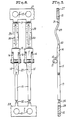
- Figure 1 shows two - individual solder bearing terminal pins 10 connected to a common carrier strip 11.
- the carrier strip may be provided with pilot holes 12 at regular intervals, as is customary, and the terminal pins may be connected to the carrier strip via break-away notches 13 for removal of the carrier strip after the terminal pins have been soldered into position.
- Each terminal pin includes an upper body portion 14, and a lower body portion 15, two fingers 16, a discrete solder mass 17, an upper contact arm 18, and a lower contact arm 19.
- the carrier strip 11 can be any length desired, carrying a great number of terminal pins.
- the terminal pins and carrier strip are preferably made by continuously stamping them from a thin sheet of metal, and during the stamping operation, the fingers 16 are bent out of the plane of the body of the terminal pin.
- each finger 16 has a curved portion.
- a partially enclosed space is formed by an inner concave side of each finger 16 with an opening to this space facing in a direction along the body portion of the terminal pin i.e. downwardly in Figure 2.
- the fingers 16 are wrapped partially around the discrete mass of solder 17, a lower end of each finger serving as a solderable portion.
- the fingers are preferably stamped to a thickness which is less than that of the body of the terminal pin. This allows the fingers 16 to be wrapped more readily around the discrete mass of solder 17.
- the wrapping can be done with sufficient force to indent the fingers into the surface of the solder to provide a firm mechanical attachment between the solder and the terminal pin which prevents the solder from becoming dislodged during shipping and handling. prior to the completion of the soldering operation.
- the fingers 16 are of a thickness which is less than the thickness of the body of the terminal pin.
- the thickness of the body portions 14 and 15 are, for convenience, usually but not necessarily, chosen to be of the same thickness as that of the upper and lower contact arms 18 and 19 respectively. This thickness may be adjusted during the stamping operation.
- the contact arms may be soldered to an adjacent printed circuit board, may have wires or other electrical components soldered to them, may serve as pin or blade connectors for an electrical plug, may have a wire or wires conventionally wire wrapped onto them, may function as spring contacts, or may have other electrical and mechanical connections where appropriate.
- the fingers 16 are preferably stamped from the same thin sheet material as the remainder of the pin, and the thickness of the fingers is reduced during the stamping operation, allowing them to be more easily formed into the appropriate shape.
- Upper contact arm 18 may be of any suitable shape. If required, it may have a square cross section suitable for a wire wrapped connection, or a round cross section for a solder connection, and it may be straight or bent out of the plane of the terminal pin as indicated in the dashed lines 26 of Figure 2 to form a spring-like side contact arm.
- Lower contact arm 19 must be of a size such as to permit it to pass through the receptacle in the substrate which requires that its largest cross sectional dimension be no larger than the largest cross section dimension of the lower body portion 15. Lower contact arm 19 may be eliminated entirely where desired, as may upper contact arm 18. In the latter case, carrier strip 11 would be attached directly to the upper body portion 14.
- the second modified form of the terminal pin is shown as having a single central finger 24 formed from a U-shaped longitudinal cut 25 along the axis of the body.
- the U-shaped longitudinal cut 25 can be extended down the axis of the lower body portion 15 to perform the same function as longitudinal slot 23 to provide a compliant pin.
- the mass of solder is in mechanical engagement with the terminal fingers in position to be melted for the formation of a bond between the terminal fingers 16, the terminal body 14 and 15 and the receptacle 20 in the substrate 21.
- the solder mass may, if desired, have a cross section of circular, square or other geometrical form, or be made from spherical pellets.
- Figure 8 has been drawn with two fingers 16, it is apparent that it can be constructed with a single central finger 24 as shown in Figures 6 and 7. It also can be constructed with or without a central longitudinal slot 30 or a longitudinal slot 23 as desired. Furthermore, a lower carrier strip 28 may be used in conjunction with any of the terminal pins shown and where such a lower carrier strip is used, the upper carrier strip is optional. Each terminal can also be made by simple stamping and assembling steps, with minimal waste of material.
Landscapes
- Engineering & Computer Science (AREA)
- Manufacturing & Machinery (AREA)
- Microelectronics & Electronic Packaging (AREA)
- Coupling Device And Connection With Printed Circuit (AREA)
- Multi-Conductor Connections (AREA)
Abstract
Claims (15)
Priority Applications (1)
| Application Number | Priority Date | Filing Date | Title |
|---|---|---|---|
| AT83902372T ATE47506T1 (de) | 1982-07-09 | 1983-06-16 | Lottragende endklemme. |
Applications Claiming Priority (2)
| Application Number | Priority Date | Filing Date | Title |
|---|---|---|---|
| US39676482A | 1982-07-09 | 1982-07-09 | |
| US396764 | 1982-07-09 |
Publications (3)
| Publication Number | Publication Date |
|---|---|
| EP0112899A1 EP0112899A1 (fr) | 1984-07-11 |
| EP0112899A4 EP0112899A4 (fr) | 1986-10-02 |
| EP0112899B1 true EP0112899B1 (fr) | 1989-10-18 |
Family
ID=23568530
Family Applications (1)
| Application Number | Title | Priority Date | Filing Date |
|---|---|---|---|
| EP83902372A Expired EP0112899B1 (fr) | 1982-07-09 | 1983-06-16 | Broche a borne portant une soudure |
Country Status (6)
| Country | Link |
|---|---|
| EP (1) | EP0112899B1 (fr) |
| CA (1) | CA1197912A (fr) |
| DE (1) | DE3380758D1 (fr) |
| DK (1) | DK54084D0 (fr) |
| IT (1) | IT1172289B (fr) |
| WO (1) | WO1984000445A1 (fr) |
Cited By (1)
| Publication number | Priority date | Publication date | Assignee | Title |
|---|---|---|---|---|
| CN106532308A (zh) * | 2015-09-10 | 2017-03-22 | 泰连德国有限公司 | 具有改进的连接凸部几何形状的金属片材零件 |
Family Cites Families (7)
| Publication number | Priority date | Publication date | Assignee | Title |
|---|---|---|---|---|
| US3915546A (en) * | 1971-06-15 | 1975-10-28 | Amp Inc | Selectively applied flowable solder apparatus, product and method of fabrication |
| US3864014A (en) * | 1972-05-01 | 1975-02-04 | Amp Inc | Coined post for solder stripe |
| US4203648A (en) * | 1977-08-15 | 1980-05-20 | North American Specialties Corp. | Solder bearing terminal |
| JPS5919416B2 (ja) * | 1978-04-27 | 1984-05-07 | イ−・アイ・デユポン・デ・ニモアス・アンド・カンパニ− | 電気用端子 |
| US4193654A (en) * | 1978-09-08 | 1980-03-18 | Amp Incorporated | Electrical connector receptacles |
| JPS5811076B2 (ja) * | 1978-12-25 | 1983-03-01 | 株式会社エルコ インタ−ナシヨナル | 電気接続子組立体 |
| US4302067A (en) * | 1980-04-18 | 1981-11-24 | Western Electric Company, Incorporated | Edge connectors for circuit cards and methods of assembly |
-
1983
- 1983-06-16 WO PCT/US1983/000951 patent/WO1984000445A1/fr not_active Ceased
- 1983-06-16 EP EP83902372A patent/EP0112899B1/fr not_active Expired
- 1983-06-16 DE DE8383902372T patent/DE3380758D1/de not_active Expired
- 1983-06-20 CA CA000430766A patent/CA1197912A/fr not_active Expired
- 1983-07-08 IT IT48654/83A patent/IT1172289B/it active
-
1984
- 1984-02-07 DK DK0540/84A patent/DK54084D0/da unknown
Cited By (2)
| Publication number | Priority date | Publication date | Assignee | Title |
|---|---|---|---|---|
| CN106532308A (zh) * | 2015-09-10 | 2017-03-22 | 泰连德国有限公司 | 具有改进的连接凸部几何形状的金属片材零件 |
| CN106532308B (zh) * | 2015-09-10 | 2020-12-01 | 泰连德国有限公司 | 具有改进的连接凸部几何形状的金属片材零件 |
Also Published As
| Publication number | Publication date |
|---|---|
| DE3380758D1 (en) | 1989-11-23 |
| IT8348654A0 (it) | 1983-07-08 |
| IT1172289B (it) | 1987-06-18 |
| EP0112899A1 (fr) | 1984-07-11 |
| EP0112899A4 (fr) | 1986-10-02 |
| DK54084A (da) | 1984-02-07 |
| WO1984000445A1 (fr) | 1984-02-02 |
| DK54084D0 (da) | 1984-02-07 |
| CA1197912A (fr) | 1985-12-10 |
Similar Documents
| Publication | Publication Date | Title |
|---|---|---|
| EP0694220B1 (fr) | Fil porteur de metal de brasage | |
| US4679889A (en) | Solder-bearing leads | |
| EP0215024B1 (fr) | Borne pourvue de soudure | |
| US6099365A (en) | Solder-holding clips for applying solder to connectors or the like | |
| US5052954A (en) | Solder-bearing terminal pin and lead | |
| US4883435A (en) | Solder-bearing terminal pin and lead | |
| US4780098A (en) | Conductive lead arrangement | |
| WO1997016870A9 (fr) | Pince a retenue de soudure pour l'application de soudure a des connecteurs | |
| US4728305A (en) | Solder-bearing leads | |
| EP0112899B1 (fr) | Broche a borne portant une soudure | |
| AU583396B2 (en) | Solder bearing leads | |
| CA2236464C (fr) | Pince a retenue de soudure pour l'application de soudure a des connecteurs | |
| CA1207856A (fr) | Pince a soudure tendre sur rive pour raccordement a un substrat | |
| EP0116073B1 (fr) | Attache de bord portant soudure | |
| JPS593502Y2 (ja) | 回路素子の接続端子台 | |
| JPH0425677B2 (fr) |
Legal Events
| Date | Code | Title | Description |
|---|---|---|---|
| PUAI | Public reference made under article 153(3) epc to a published international application that has entered the european phase |
Free format text: ORIGINAL CODE: 0009012 |
|
| 17P | Request for examination filed |
Effective date: 19840210 |
|
| AK | Designated contracting states |
Designated state(s): AT BE CH DE FR GB LI LU NL SE |
|
| RIN1 | Information on inventor provided before grant (corrected) |
Inventor name: SEIDLER, JACK |
|
| A4 | Supplementary search report drawn up and despatched |
Effective date: 19861002 |
|
| 17Q | First examination report despatched |
Effective date: 19870428 |
|
| GRAA | (expected) grant |
Free format text: ORIGINAL CODE: 0009210 |
|
| AK | Designated contracting states |
Kind code of ref document: B1 Designated state(s): AT BE CH DE FR GB LI LU NL SE |
|
| PG25 | Lapsed in a contracting state [announced via postgrant information from national office to epo] |
Ref country code: SE Effective date: 19891018 Ref country code: LI Effective date: 19891018 Ref country code: CH Effective date: 19891018 Ref country code: AT Effective date: 19891018 |
|
| REF | Corresponds to: |
Ref document number: 47506 Country of ref document: AT Date of ref document: 19891115 Kind code of ref document: T |
|
| REF | Corresponds to: |
Ref document number: 3380758 Country of ref document: DE Date of ref document: 19891123 |
|
| ET | Fr: translation filed | ||
| REG | Reference to a national code |
Ref country code: CH Ref legal event code: PL |
|
| PGFP | Annual fee paid to national office [announced via postgrant information from national office to epo] |
Ref country code: SE Payment date: 19900522 Year of fee payment: 8 |
|
| PLBE | No opposition filed within time limit |
Free format text: ORIGINAL CODE: 0009261 |
|
| STAA | Information on the status of an ep patent application or granted ep patent |
Free format text: STATUS: NO OPPOSITION FILED WITHIN TIME LIMIT |
|
| 26N | No opposition filed | ||
| EPTA | Lu: last paid annual fee | ||
| PGFP | Annual fee paid to national office [announced via postgrant information from national office to epo] |
Ref country code: LU Payment date: 19950501 Year of fee payment: 13 |
|
| PG25 | Lapsed in a contracting state [announced via postgrant information from national office to epo] |
Ref country code: LU Free format text: LAPSE BECAUSE OF NON-PAYMENT OF DUE FEES Effective date: 19960616 |
|
| PGFP | Annual fee paid to national office [announced via postgrant information from national office to epo] |
Ref country code: NL Payment date: 20000629 Year of fee payment: 18 |
|
| PGFP | Annual fee paid to national office [announced via postgrant information from national office to epo] |
Ref country code: BE Payment date: 20000814 Year of fee payment: 18 |
|
| PGFP | Annual fee paid to national office [announced via postgrant information from national office to epo] |
Ref country code: FR Payment date: 20010611 Year of fee payment: 19 Ref country code: DE Payment date: 20010611 Year of fee payment: 19 |
|
| PGFP | Annual fee paid to national office [announced via postgrant information from national office to epo] |
Ref country code: GB Payment date: 20010613 Year of fee payment: 19 |
|
| PG25 | Lapsed in a contracting state [announced via postgrant information from national office to epo] |
Ref country code: BE Free format text: LAPSE BECAUSE OF NON-PAYMENT OF DUE FEES Effective date: 20010630 |
|
| BERE | Be: lapsed |
Owner name: NORTH AMERICAN SPECIALITIES CORP. Effective date: 20010630 |
|
| PG25 | Lapsed in a contracting state [announced via postgrant information from national office to epo] |
Ref country code: NL Free format text: LAPSE BECAUSE OF NON-PAYMENT OF DUE FEES Effective date: 20020101 |
|
| REG | Reference to a national code |
Ref country code: GB Ref legal event code: IF02 |
|
| NLV4 | Nl: lapsed or anulled due to non-payment of the annual fee |
Effective date: 20020101 |
|
| PG25 | Lapsed in a contracting state [announced via postgrant information from national office to epo] |
Ref country code: GB Free format text: LAPSE BECAUSE OF NON-PAYMENT OF DUE FEES Effective date: 20020616 |
|
| PG25 | Lapsed in a contracting state [announced via postgrant information from national office to epo] |
Ref country code: DE Free format text: LAPSE BECAUSE OF NON-PAYMENT OF DUE FEES Effective date: 20030101 |
|
| GBPC | Gb: european patent ceased through non-payment of renewal fee |
Effective date: 20020616 |
|
| PG25 | Lapsed in a contracting state [announced via postgrant information from national office to epo] |
Ref country code: FR Free format text: LAPSE BECAUSE OF NON-PAYMENT OF DUE FEES Effective date: 20030228 |
|
| REG | Reference to a national code |
Ref country code: FR Ref legal event code: ST |