EP0113186A2 - Procédé de fabrication d'un fil supraconducteur à filament mince en alliage de Nb-Ti - Google Patents
Procédé de fabrication d'un fil supraconducteur à filament mince en alliage de Nb-Ti Download PDFInfo
- Publication number
- EP0113186A2 EP0113186A2 EP83307260A EP83307260A EP0113186A2 EP 0113186 A2 EP0113186 A2 EP 0113186A2 EP 83307260 A EP83307260 A EP 83307260A EP 83307260 A EP83307260 A EP 83307260A EP 0113186 A2 EP0113186 A2 EP 0113186A2
- Authority
- EP
- European Patent Office
- Prior art keywords
- wire
- atomic
- wires
- temperature
- alloy
- Prior art date
- Legal status (The legal status is an assumption and is not a legal conclusion. Google has not performed a legal analysis and makes no representation as to the accuracy of the status listed.)
- Granted
Links
- 229910045601 alloy Inorganic materials 0.000 title claims abstract description 40
- 239000000956 alloy Substances 0.000 title claims abstract description 40
- 229910020012 Nb—Ti Inorganic materials 0.000 title claims abstract description 20
- 238000004519 manufacturing process Methods 0.000 title claims abstract description 10
- 239000010936 titanium Substances 0.000 claims abstract description 14
- 229910052719 titanium Inorganic materials 0.000 claims abstract description 14
- 238000010622 cold drawing Methods 0.000 claims abstract description 13
- 239000010955 niobium Substances 0.000 claims abstract description 13
- RTAQQCXQSZGOHL-UHFFFAOYSA-N Titanium Chemical compound [Ti] RTAQQCXQSZGOHL-UHFFFAOYSA-N 0.000 claims abstract description 11
- 229910052758 niobium Inorganic materials 0.000 claims abstract description 10
- GUCVJGMIXFAOAE-UHFFFAOYSA-N niobium atom Chemical compound [Nb] GUCVJGMIXFAOAE-UHFFFAOYSA-N 0.000 claims abstract description 10
- 239000003381 stabilizer Substances 0.000 claims abstract description 9
- 229910052715 tantalum Inorganic materials 0.000 claims abstract description 9
- 229910052721 tungsten Inorganic materials 0.000 claims abstract description 9
- GUVRBAGPIYLISA-UHFFFAOYSA-N tantalum atom Chemical compound [Ta] GUVRBAGPIYLISA-UHFFFAOYSA-N 0.000 claims abstract description 8
- 229910052735 hafnium Inorganic materials 0.000 claims abstract description 7
- VBJZVLUMGGDVMO-UHFFFAOYSA-N hafnium atom Chemical compound [Hf] VBJZVLUMGGDVMO-UHFFFAOYSA-N 0.000 claims abstract description 7
- WFKWXMTUELFFGS-UHFFFAOYSA-N tungsten Chemical compound [W] WFKWXMTUELFFGS-UHFFFAOYSA-N 0.000 claims abstract description 7
- 239000010937 tungsten Substances 0.000 claims abstract description 7
- 238000000034 method Methods 0.000 claims description 36
- 238000007669 thermal treatment Methods 0.000 claims description 31
- 238000001816 cooling Methods 0.000 claims description 12
- 238000001125 extrusion Methods 0.000 claims description 12
- RYGMFSIKBFXOCR-UHFFFAOYSA-N Copper Chemical compound [Cu] RYGMFSIKBFXOCR-UHFFFAOYSA-N 0.000 claims description 3
- 229910052802 copper Inorganic materials 0.000 claims description 3
- 239000010949 copper Substances 0.000 claims description 3
- 239000011261 inert gas Substances 0.000 claims description 2
- XAGFODPZIPBFFR-UHFFFAOYSA-N aluminium Chemical compound [Al] XAGFODPZIPBFFR-UHFFFAOYSA-N 0.000 claims 1
- 229910052782 aluminium Inorganic materials 0.000 claims 1
- 239000001307 helium Substances 0.000 description 6
- 229910052734 helium Inorganic materials 0.000 description 6
- SWQJXJOGLNCZEY-UHFFFAOYSA-N helium atom Chemical compound [He] SWQJXJOGLNCZEY-UHFFFAOYSA-N 0.000 description 6
- 239000000203 mixture Substances 0.000 description 5
- IJGRMHOSHXDMSA-UHFFFAOYSA-N Atomic nitrogen Chemical compound N#N IJGRMHOSHXDMSA-UHFFFAOYSA-N 0.000 description 4
- 239000002244 precipitate Substances 0.000 description 4
- 229910002056 binary alloy Inorganic materials 0.000 description 2
- 150000001875 compounds Chemical class 0.000 description 2
- 239000005457 ice water Substances 0.000 description 2
- 239000007788 liquid Substances 0.000 description 2
- 229910052757 nitrogen Inorganic materials 0.000 description 2
- CURLTUGMZLYLDI-UHFFFAOYSA-N Carbon dioxide Chemical compound O=C=O CURLTUGMZLYLDI-UHFFFAOYSA-N 0.000 description 1
- 239000000654 additive Substances 0.000 description 1
- 230000000996 additive effect Effects 0.000 description 1
- 238000009835 boiling Methods 0.000 description 1
- 229960004424 carbon dioxide Drugs 0.000 description 1
- 235000011089 carbon dioxide Nutrition 0.000 description 1
- 239000002131 composite material Substances 0.000 description 1
- 230000006866 deterioration Effects 0.000 description 1
- 230000000694 effects Effects 0.000 description 1
- 238000002474 experimental method Methods 0.000 description 1
- 230000004927 fusion Effects 0.000 description 1
- 239000000463 material Substances 0.000 description 1
- 238000005259 measurement Methods 0.000 description 1
- 229910052751 metal Inorganic materials 0.000 description 1
- 229910000657 niobium-tin Inorganic materials 0.000 description 1
- 229910000999 vanadium-gallium Inorganic materials 0.000 description 1
Images


Classifications
-
- H—ELECTRICITY
- H10—SEMICONDUCTOR DEVICES; ELECTRIC SOLID-STATE DEVICES NOT OTHERWISE PROVIDED FOR
- H10N—ELECTRIC SOLID-STATE DEVICES NOT OTHERWISE PROVIDED FOR
- H10N60/00—Superconducting devices
- H10N60/80—Constructional details
- H10N60/85—Superconducting active materials
-
- H—ELECTRICITY
- H10—SEMICONDUCTOR DEVICES; ELECTRIC SOLID-STATE DEVICES NOT OTHERWISE PROVIDED FOR
- H10N—ELECTRIC SOLID-STATE DEVICES NOT OTHERWISE PROVIDED FOR
- H10N60/00—Superconducting devices
- H10N60/01—Manufacture or treatment
- H10N60/0156—Manufacture or treatment of devices comprising Nb or an alloy of Nb with one or more of the elements of group IVB, e.g. titanium, zirconium or hafnium
-
- Y—GENERAL TAGGING OF NEW TECHNOLOGICAL DEVELOPMENTS; GENERAL TAGGING OF CROSS-SECTIONAL TECHNOLOGIES SPANNING OVER SEVERAL SECTIONS OF THE IPC; TECHNICAL SUBJECTS COVERED BY FORMER USPC CROSS-REFERENCE ART COLLECTIONS [XRACs] AND DIGESTS
- Y10—TECHNICAL SUBJECTS COVERED BY FORMER USPC
- Y10S—TECHNICAL SUBJECTS COVERED BY FORMER USPC CROSS-REFERENCE ART COLLECTIONS [XRACs] AND DIGESTS
- Y10S505/00—Superconductor technology: apparatus, material, process
- Y10S505/80—Material per se process of making same
- Y10S505/815—Process of making per se
-
- Y—GENERAL TAGGING OF NEW TECHNOLOGICAL DEVELOPMENTS; GENERAL TAGGING OF CROSS-SECTIONAL TECHNOLOGIES SPANNING OVER SEVERAL SECTIONS OF THE IPC; TECHNICAL SUBJECTS COVERED BY FORMER USPC CROSS-REFERENCE ART COLLECTIONS [XRACs] AND DIGESTS
- Y10—TECHNICAL SUBJECTS COVERED BY FORMER USPC
- Y10S—TECHNICAL SUBJECTS COVERED BY FORMER USPC CROSS-REFERENCE ART COLLECTIONS [XRACs] AND DIGESTS
- Y10S505/00—Superconductor technology: apparatus, material, process
- Y10S505/825—Apparatus per se, device per se, or process of making or operating same
- Y10S505/917—Mechanically manufacturing superconductor
- Y10S505/918—Mechanically manufacturing superconductor with metallurgical heat treating
- Y10S505/919—Reactive formation of superconducting intermetallic compound
- Y10S505/921—Metal working prior to treating
-
- Y—GENERAL TAGGING OF NEW TECHNOLOGICAL DEVELOPMENTS; GENERAL TAGGING OF CROSS-SECTIONAL TECHNOLOGIES SPANNING OVER SEVERAL SECTIONS OF THE IPC; TECHNICAL SUBJECTS COVERED BY FORMER USPC CROSS-REFERENCE ART COLLECTIONS [XRACs] AND DIGESTS
- Y10—TECHNICAL SUBJECTS COVERED BY FORMER USPC
- Y10S—TECHNICAL SUBJECTS COVERED BY FORMER USPC CROSS-REFERENCE ART COLLECTIONS [XRACs] AND DIGESTS
- Y10S505/00—Superconductor technology: apparatus, material, process
- Y10S505/825—Apparatus per se, device per se, or process of making or operating same
- Y10S505/917—Mechanically manufacturing superconductor
- Y10S505/928—Metal deforming
- Y10S505/929—Metal deforming by extruding
-
- Y—GENERAL TAGGING OF NEW TECHNOLOGICAL DEVELOPMENTS; GENERAL TAGGING OF CROSS-SECTIONAL TECHNOLOGIES SPANNING OVER SEVERAL SECTIONS OF THE IPC; TECHNICAL SUBJECTS COVERED BY FORMER USPC CROSS-REFERENCE ART COLLECTIONS [XRACs] AND DIGESTS
- Y10—TECHNICAL SUBJECTS COVERED BY FORMER USPC
- Y10S—TECHNICAL SUBJECTS COVERED BY FORMER USPC CROSS-REFERENCE ART COLLECTIONS [XRACs] AND DIGESTS
- Y10S505/00—Superconductor technology: apparatus, material, process
- Y10S505/825—Apparatus per se, device per se, or process of making or operating same
- Y10S505/917—Mechanically manufacturing superconductor
- Y10S505/928—Metal deforming
- Y10S505/93—Metal deforming by drawing
-
- Y—GENERAL TAGGING OF NEW TECHNOLOGICAL DEVELOPMENTS; GENERAL TAGGING OF CROSS-SECTIONAL TECHNOLOGIES SPANNING OVER SEVERAL SECTIONS OF THE IPC; TECHNICAL SUBJECTS COVERED BY FORMER USPC CROSS-REFERENCE ART COLLECTIONS [XRACs] AND DIGESTS
- Y10—TECHNICAL SUBJECTS COVERED BY FORMER USPC
- Y10T—TECHNICAL SUBJECTS COVERED BY FORMER US CLASSIFICATION
- Y10T29/00—Metal working
- Y10T29/49—Method of mechanical manufacture
- Y10T29/49002—Electrical device making
- Y10T29/49014—Superconductor
Definitions
- This invention relates to improvements in a method of manufacturing a fine multi-filamentary Nb-Ti based superconducting wire consisting of a Nb-Ti alloy containing one or more metal elements selected from a group consisting of hafnium, tantalum and tungsten.
- Nb-Ti binary alloy wires as superconducting wires for magnets providing magnetic field of at most 8 or 9 teslas while using compound wires of Nb 3 Sn or V 3 G a having satisfactory properties as superconducting wires for magnets providing magnetic field in a range of 9 to 13 teslas.
- the superconducting wire is subject to a greater electromagnetic force, with the result that the stress damage done to the properties of the compound superconducting wire has become a serious problem.
- marked progress has been achieved recently in the field of cooling technique, e.g., pressurized superfluid helium cooling under pressure, making it possible to achieve a temperature less than 4.2 K easily.
- the technique of adding another element to a Nb-Ti superconducting wire and using said superconducting wire under temperatures lower than 4.2 K, particularly, within a superfluid helium temperature range, has come to attract attentions in this field as a measure for solving the stress damage problem and obtaining a magnet generating a high magnetic field.
- the NbTi based alloy has a superior stress tolerance, and there is a theoretical forecast that addition of heavy elements such as hafnium, tantalum and tungsten to a Nb-Ti alloy permits an upper critical magnetic field higher than that of Nb-Ti binary alloy to be attained in the superfluidity temperature range of helium, and extensive experiments have been conducted on bulk materials of such alloys.
- An object of the invention is to provide a method of manufacturing a fine multifilamentary Nb-Ti based superconducting wire having superior superconducting properties, e.g., critical current, to those of the prior art Nb-Ti wires.
- the method of manufacturing a fine multifilamentary Nb-Ti based superconducting wire according to the invention consists of three distinct steps.
- a Nb-Ti based alloy is prepared by adding one or more elements selected from a group consisting of hafnium, tantalum and tungsten in an amount not exceeding 30 atomic % to a Nb-Ti alloy composed of 10 to 50 atomic % of niobium and 40 to 75 atomic % of titanium.
- An alloy wire is then formed from the resultant alloy by such process as extrusion and/or drawing.
- the amounts of the components of the alloy are set in the ranges noted above for the following reasons. If the amount of niobium is below 10 atmoic % or above 50 atomic %, a superconducting wire having a sufficiently high critial temperature and upper critical magnetic field cannot be obtained.
- a more preferable range of the amount of niobium is 15 to 40 atomic %.
- titanium if its amount is below 40 atomic %, fine precipitates which are necessary for increasing the critical current cannot be formed in the alloy.
- the amount of titanium in excess of 75 atomic % deteriorates the workability of the alloy.
- a more preferable range of the amount of titanium is 45 to 75 %.
- the additive element if its amount exceeds 30 atomic %, the workability of the alloy is extremely deteriorated and the critical current thereof is reduced.
- the amount is preferably above 0.5 atmoic % more perferably 0.5 to 20 atmic %, to obtain a superconducting wire having sufficiently high upper critical magnetic field in the superfluidity temperature of helium.
- the alloy wire obtained in the first step is covered with a stabilizer, and the resultant wire is subjected to extrusion and/or cold drawing.
- a plurality of, e.g. several hundred to tens of thousand, the stabilizer-clad alloy wires thus obtained are bundled, the resultant bundle being covered again with a stabilizer, the resultant composite being subjected to extrusion and/or drawing to obtain a multifilamentary wire. Additional processes of covering with stabilizer and extrusion and/or drawing may be carried out repeatedly until a predetermined diameter of the filament is obtained.
- the multifilamentary wire obtained in the second step is thermally treated at a temperature of 250 to 600°C, more preferably 300 to 500°C, and is then drawn with reduction rate of 30 to 99.9 %, thereby obtaining a fine multifilamentary superconducting wire. If necessary, the third step may be repeatedly carried out a plurality of times.
- the reduction rate D is given as
- the reason for setting the temperature of the thermal treatment in the third step to 250 to 600°C is as follows. If it is below 250°C, precipitates cannot be formed in the alloy at a density necessary to obtain sufficiently high critial current. If it exceeds 600°C, the precipitates grow larger to result in the reduction of the critical current.
- the thermal treatment may be carried out in an inert gas atmosphere or vacuum for 2 to 1,000 hours.
- the drawing process with a reduction rate of 30 to 99.9 % in the third step will introduce a number of dislocations into the alloy structure, which, together with the precipitates formed by the thermal treatment, have an effect of markedly improving the critical current in the neighborhood of the upper critical magnetic field.
- the superconducting wire will exhibit excellent critical current properties in a high magnetic field when it is used in a temperature range below 2.2 K, i.e., the superfluidity temperature range of helium.
- the reason for setting the reduction rate to 30 to 99.9 % is as follows. If it is below 30 %, insufficient dislocations are introduced into the alloy structure. Increasing it beyond 99.9 % results in pronounced breakage of filaments.
- the drawing in the third step may be done either as cold or warm drawing.
- cold drawing When cold drawing is done, greater number of dislocations can be introduced into the alloy structure, improving the critical current per filament.
- the warm drawing is preferably carried out at a temperature of 300°C or less. If the temperature exceeds 300°C, the dislocations introduced by the warm drawing are prominently reduced so that sufficient improvement of the critical current cannot be obtained.
- the drawing may be carried out as a combination of cold and warm drawing processes.
- the temperature of the multifilamentary wire is extremely elevated when the wire passes through the drawing die. This temperature rise results in reduction of dislocations.
- each alloy rod was inserted into a copper tube (i.e., stabilizer) with an outer diamter of 40 mm, and the resultant copper-clad rod was cold-drawn.
- a number of copper-clad wires were thus prepared. 295 such copper-clad wires were then inserted into a copper tube with an outer diameter of 50 mm, and the resultant system was subjected to hydraulic extrusion and cold drawing, thereby obtaining a multifilamentary wire with an outer diameter of 8 mm. At this moment, the reduction ration of the filament was about 10 4 (second step).
- the individual multifilamentary wires were than subjected to the third step under conditions listed in the Table below, thereby obtaining 27 different fine multifilamentary Nb-Ti based superconducting wires.
- the conditions of the step 3 as shown in the Table the samples lA to 9A were subjected to the sole thermal treatment, the samples 1B to 9B were subjected to a process consisting of thermal treatment and cold drawing three times, and the samples 1C to 9C were subjected to a process consisting of thermal treatment and warm drawing three times.
- the drawing was carried out from a state, at which the reduction ratio (i.e., the sectional area of the filament before drawing divided by the sectional area of the same after drawing) was about 10 4 (outer diameter: 8 mm) in the first and second steps, until the reduction ratio was about 10 6 (outer diameter: 0.8 mm) in the final drawing in the third step.
- the drawing was done up to a reduction ratio of about 10 6 (outer diameter: 0.8 mm) in the first and second steps.
- the superconducting wires obtained from the alloys having compositions in the range according to the invention through three times of a combination process consisting of thermal treatment and cold drawing i.e., samples 1B to 6B
- samples 1B to 6B are extremely improved in the critical current density over the superconducting wires, which are obtained through the sole thermal treatment provided on the multifilamentary wires manufactured from the alloys of the same compositions (i.e., samples lA to 6A), becuase of introduction of more dislocations into the alloy structure although the breakage of filaments is slightly increased.
- the superconducting wires obtained from the multifilamentary wires made of alloys of the same compositions by carrying out the combination process consisting of thermal treatment and warm drawing three times are extremely improved in the critical current density because the breakage of filaments is reduced.
- Multifilamentary wires (consisting of 295 filaments) were manufactured from an alloy composed of 35 atmoic % of niobium, 62 atomic % of titanium and 3 atomic % of hafnium. These multifilamentary wires were processed in various ways as the third step to obtain five different kinds of fine multifilamentary Nb-Ti-Hf superconducting wires.
- line A represents the property of a superconducting wire obtained from a multifilamentary wire, which has been obtained through cold drawing up to a reduction ratio of about 10 6 in the second step, through the sole thermal treatment carried out under the same conditions as those with the samples 1A to 9A in Example 1.
- Line B represents the property of a superconducting wire obtained by carrying out the combination process of thermal treatment and cold drawing three times under the same conditions as with the samples 1B to 9B in Example 1.
- Lines C l to C 3 represent the properties of superconducting wires obtained by carrying out the combination process of thermal treatment and warm drawing under the same conditions as with the samples 1C to 9C in Example 1 once, twice and three times respectively.
- the superconducting wires obtained by carrying out the third step according to the invention i.e., those of lines B and C 1 to C 3
- the critical current density is more improved as the thermal treatment and drawing are carried out repeatedly.
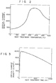
- M ultifilamentary wires (consisting of 295 filaments) were manufactured from an alloy composed of 20 atomic % of niobium, 65 atmoic % of titanium and 15 atomic % of tantalum. In the manfactured of these wires, extrusion and drawing were done to a reduction ratio of about 10 4 in the second step. These wires were subjected to a combination process consisting of thermal treatment at various temperatures for 50 hours and warm drawing up to a reduction rate of 80 % at 200°C. The combination process was conducted three times to obtain fine filamentary Nb-Ti-Ta superconducting wires.
- the critial current density of the superconducting wires at a temperature of 1.8 K and in a magnetic field of 10 tesles was measured, and its temperature dependency on the temperature of the thermal treatment was examined. The results were shown in Fig. 2. As is obvious from the graph of Fig. 2, high critical current density can be obtained when the temperature of the thermal treatment is 250 to 600°C.
- Fine multifilamentary superconducting wires (Nb: 20 atomic %, Ti: 65 atomic %, Ta: 15 atomic %) were produced by the same method as in Example 3 except that the temperature of the thermal treatment was set to 350°C and the period of thermal treatment was set to various values.
- the critical current density of the superconducting wires thus obtained was measured at a temperature of 1.8 K and in a magnetic field of 10 teslas, and its dependency on the temperature of the thermal treatment was examined. The result is shown in Fig. 3.
- Multifilamentary wires (consisting of 295 filaments) were produced from an alloy composed of 35 atomic % of niobium, 60 atomic % of titanium and 5 atomic % of tungsten by the same method as in Example 1. In the manufacture of these wires, extrusion and drawing to a reduction ratio of about 10 4 were done in the first and second steps. These wires were subjected to the same third step as in Example 3 except that the temperature of thermal treatment was set to 350°C and the reduction rate of warm drawing was set to various values,, thus obtaining fine multifilamentary superconducting wires. Since the reduction rate was changed in a wide range, the combination process in the third step was carried out only once.
- the critical current density of the superconducting wires was measured at a temperature of 1.8 K and in a magnetic field of 10 teslas, and its dependency on the reduction rate of the warm drawing was examined. The results are shown in Fig. 4. As is obvious from the graph of Fig. 4, high critical current density can be obtained when the reduction rate of the warm drawing is 30 to 99.9 %. Further, it was confirmed that even in the case of cold drawing high critical current density could be obtained with a reduction rate of 30 to 99.9 %.
- Fine multifilamentary superconducting wires Nb: 35 atomic %, Ti: 60 atomic %, W: 5 atomic %) were produced by the same method as in Example 5 except that the reduction rate of warm drawing was set to 80 %, the temperature condition of the warm drawing was set to various values, and the combination process was carried out three times.
- the critical current density of the superconducting wires thus obtained was measured at a temperature of 1.8 K and in a magnetic field of 10 teslas, and its dependency on the temperature of the warm drawing was examined. The results are shown in Fig. 5. As is obvious from Fig. 5, high critical current density could be obtained when the temperature in the warm drawing is 300°C or less.
- Fine multifilamentary superconducting wires (consisting of 295 filaments, Nb: 35 atomic %, T i: 60 atomic %, W: 5 atomic %) were obtained in the same manner as in Example 5.
- the extrusion and drawing in the first and second steps were done to a reduction ratio of about 10 4 .
- These wires were subjected to a combination process consisting of thermal treatment at 350°C and 50 hours and drawing with a reduction rate of 80% with cooling after passing through the, die.
- the combination process was done three times to obtain fine filamentary superconducting wires.
- the cooling of the wires after passing through the die was carried out under three different conditions, i.e., cooling down to room temperature, cooling down to 0°C using ice water, and cooling down to -196°C using liquid nitrogen.
- the critical current density of the superconducting wires was measured at a temperature of 1.8 K and in a magnetic field of 10 teslas, and its dependency on the cooling temperature after passing through the die was examined. The results are shown in Fig. 3. It will be seen from the Figure that the critical current density can be improved by cooling after the drawing in the third step.
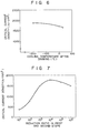
- multifilamentary wires (each consisting of 295 filaments) were produced from an alloy composed of 20 atomic % of niobium, 65 atomic % of titanium and 15 atomic % of tantalum with the reduction ratio of 10 1 to 10 6 in the first and second steps. These wires were subjected to a combination process consisting of thermal treatment at 350°C for 50 hours and warm drawing with a reduction rate of 50 % and at a temperature of 200°C. The combination process was done three times to obtain fine multifilamentary superconducting wires.
- the critical current density of the superconducting wires thus obtained were measured at a temperature of 1.8 K and in a magnetic field of 10 teslas, and its dependency on the reduction ratio of extrusion and drawing in the first and second steps was examined. The results are shown in Fig. 7. As is obvious from the graph of Fig. 7, high critical current density can be obtained when the reduction ratio of extrusion and drawing in the first and second steps is 10 3 to 10 6 .
- the invention it is possible to obtain a fine multifilamentary Nb-Ti based superconducting wire having far superior critical current properties to those of the prior art Nb-Ti superconducting wires in the superfluidity temperature range of hellium (i.e., no higher than 2.2 K). It is thus possible to increase the magnetic field and reduce the size of the superconducting magnets. Further, the superconducting wire obtained by the method according to the invention is less subject to deterioration by stress, so that it can be very effectively utilized as large size superconducting magnets used for nuclear fusion reactors and accelerators.
Landscapes
- Engineering & Computer Science (AREA)
- Manufacturing & Machinery (AREA)
- Superconductors And Manufacturing Methods Therefor (AREA)
Applications Claiming Priority (2)
| Application Number | Priority Date | Filing Date | Title |
|---|---|---|---|
| JP207642/82 | 1982-11-29 | ||
| JP57207642A JPS5998411A (ja) | 1982-11-29 | 1982-11-29 | 極細多芯Nb―Ti系超電導線の製造方法 |
Publications (4)
| Publication Number | Publication Date |
|---|---|
| EP0113186A2 true EP0113186A2 (fr) | 1984-07-11 |
| EP0113186A3 EP0113186A3 (en) | 1984-10-03 |
| EP0113186B1 EP0113186B1 (fr) | 1986-10-29 |
| EP0113186B2 EP0113186B2 (fr) | 1990-07-25 |
Family
ID=16543157
Family Applications (1)
| Application Number | Title | Priority Date | Filing Date |
|---|---|---|---|
| EP83307260A Expired - Lifetime EP0113186B2 (fr) | 1982-11-29 | 1983-11-29 | Procédé de fabrication d'un fil supraconducteur à filament mince en alliage de Nb-Ti |
Country Status (4)
| Country | Link |
|---|---|
| US (1) | US4508578A (fr) |
| EP (1) | EP0113186B2 (fr) |
| JP (1) | JPS5998411A (fr) |
| DE (1) | DE3367303D1 (fr) |
Cited By (3)
| Publication number | Priority date | Publication date | Assignee | Title |
|---|---|---|---|---|
| EP0226826A3 (en) * | 1985-11-19 | 1988-11-09 | Nippon Seisen Co., Ltd. | Method for making titanium-nickel alloys, compound material used therein and titanium-nickel alloys obtained by this method |
| EP0480427A1 (fr) * | 1990-10-12 | 1992-04-15 | Nippon Seisen Co., Ltd. | Fil de guidage pour un cathéter |
| US5238004A (en) * | 1990-04-10 | 1993-08-24 | Boston Scientific Corporation | High elongation linear elastic guidewire |
Families Citing this family (5)
| Publication number | Priority date | Publication date | Assignee | Title |
|---|---|---|---|---|
| JPH0285327A (ja) * | 1988-09-19 | 1990-03-26 | Chisato Ikeda | 難加工性合金の成形品を製造する方法 |
| US4959279A (en) * | 1989-01-17 | 1990-09-25 | The Furukawa Electric Co., Ltd. | Superconducting wire containing multifilamentary superconducting alloy |
| US20030135971A1 (en) * | 1997-11-12 | 2003-07-24 | Michael Liberman | Bundle draw based processing of nanofibers and method of making |
| US6402859B1 (en) * | 1999-09-10 | 2002-06-11 | Terumo Corporation | β-titanium alloy wire, method for its production and medical instruments made by said β-titanium alloy wire |
| CN121726160B (zh) * | 2026-02-26 | 2026-04-24 | 宁夏东方钽业股份有限公司 | 一种铌钛超导线材及其制备方法 |
Family Cites Families (7)
| Publication number | Priority date | Publication date | Assignee | Title |
|---|---|---|---|---|
| DE1287666B (fr) * | 1964-11-20 | 1969-01-23 | ||
| US3671226A (en) * | 1966-02-28 | 1972-06-20 | Mitsubishi Electric Corp | Superconductive alloys |
| NL135707C (fr) * | 1966-05-04 | |||
| GB1170645A (en) * | 1967-09-28 | 1969-11-12 | Imp Metal Ind Kynoch Ltd | Improvements relating to Electrical Conductors |
| US3837066A (en) * | 1973-02-14 | 1974-09-24 | Atomic Energy Commission | Method of extruding aluminum coated nb-ti |
| US4109374A (en) * | 1975-08-28 | 1978-08-29 | Aluminum Company Of America | Superconductor composite and method of making the same |
| US4148129A (en) * | 1976-11-01 | 1979-04-10 | Airco, Inc. | Aluminum-stabilized multifilamentary superconductor and method of its manufacture |
-
1982
- 1982-11-29 JP JP57207642A patent/JPS5998411A/ja active Granted
-
1983
- 1983-11-29 DE DE8383307260T patent/DE3367303D1/de not_active Expired
- 1983-11-29 US US06/556,099 patent/US4508578A/en not_active Expired - Lifetime
- 1983-11-29 EP EP83307260A patent/EP0113186B2/fr not_active Expired - Lifetime
Non-Patent Citations (1)
| Title |
|---|
| None |
Cited By (4)
| Publication number | Priority date | Publication date | Assignee | Title |
|---|---|---|---|---|
| EP0226826A3 (en) * | 1985-11-19 | 1988-11-09 | Nippon Seisen Co., Ltd. | Method for making titanium-nickel alloys, compound material used therein and titanium-nickel alloys obtained by this method |
| US5238004A (en) * | 1990-04-10 | 1993-08-24 | Boston Scientific Corporation | High elongation linear elastic guidewire |
| EP0480427A1 (fr) * | 1990-10-12 | 1992-04-15 | Nippon Seisen Co., Ltd. | Fil de guidage pour un cathéter |
| US5230348A (en) * | 1990-10-12 | 1993-07-27 | Nippon Seisen Co., Ltd. | Guide wire for a catheter |
Also Published As
| Publication number | Publication date |
|---|---|
| DE3367303D1 (en) | 1986-12-04 |
| EP0113186A3 (en) | 1984-10-03 |
| EP0113186B1 (fr) | 1986-10-29 |
| JPH0440806B2 (fr) | 1992-07-06 |
| US4508578A (en) | 1985-04-02 |
| JPS5998411A (ja) | 1984-06-06 |
| EP0113186B2 (fr) | 1990-07-25 |
Similar Documents
| Publication | Publication Date | Title |
|---|---|---|
| EP0140356B1 (fr) | Procédé de fabrication de supraconduc teurs à filaments multiples | |
| US4917965A (en) | Multifilament Nb3 Al superconducting linear composite articles | |
| US4746581A (en) | Multifilamentary superconductive wires composed of filaments Nb3 Sn or V3 Ga clad in copper or copper alloys and process for manufacturing such wires | |
| EP0113186B1 (fr) | Procédé de fabrication d'un fil supraconducteur à filament mince en alliage de Nb-Ti | |
| EP0045584B1 (fr) | Procédé de fabrication de supraconducteurs à filaments multiples | |
| US5554448A (en) | Wire for Nb3 X superconducting wire | |
| US5001020A (en) | Multifilament superconducting wire of NB3 AL | |
| US5230748A (en) | Superconductor and process of manufacture | |
| DE69421197T2 (de) | Verfahren zur Herstellung eines Nb3X supraleitenden Drahtes | |
| JP3063025B2 (ja) | Nb3Sn超電導線およびその製造方法 | |
| RU2069399C1 (ru) | Способ изготовления композитного сверхпроводника на основе соединения nb*003sn | |
| US4324842A (en) | Superconducting wire with improved strain characteristics | |
| US3996662A (en) | Method for the manufacture of a superconductor having an intermetallic two element compound | |
| Thoner et al. | Nb/sub 3/Sn multifilamentary superconductors: an updated comparison of different manufacturing routes | |
| US3437459A (en) | Composite superconductor having a core of superconductivity metal with a nonsuperconductive coat | |
| US6571453B1 (en) | Method for producing a superconductor, in strip form, having a high-Tc superconductor material | |
| US4343867A (en) | Superconducting wire with improved strain characteristics | |
| Wong et al. | Variable composition NbTi superconductors produced by artificial pinning center process | |
| US5891585A (en) | Nb3 Al multi-filamentary superconducting wire | |
| Iijima et al. | Cu-added Nb/sub 3/Al multifilamentary superconductors having high J/sub c/in high fields | |
| Pyon et al. | Some effects of matrix additions to internal tin processed multifilamentary Nb/sub 3/Sn superconductors | |
| Hong et al. | High current density of NbTi composite | |
| JPH0850827A (ja) | 超伝導体の製造方法 | |
| JPH0636331B2 (ja) | Nb▲下3▼A1化合物超電導線材の製造法 | |
| EP0169078A2 (fr) | Supraconducteur fabriqué à l'aide du composé Nb3Sn |
Legal Events
| Date | Code | Title | Description |
|---|---|---|---|
| PUAI | Public reference made under article 153(3) epc to a published international application that has entered the european phase |
Free format text: ORIGINAL CODE: 0009012 |
|
| 17P | Request for examination filed |
Effective date: 19831212 |
|
| AK | Designated contracting states |
Designated state(s): DE FR GB |
|
| PUAL | Search report despatched |
Free format text: ORIGINAL CODE: 0009013 |
|
| RAP1 | Party data changed (applicant data changed or rights of an application transferred) |
Owner name: KABUSHIKI KAISHA TOSHIBA Owner name: DIRECTOR, NATIONAL RESEARCH INSTITUTE FOR METALS |
|
| AK | Designated contracting states |
Designated state(s): DE FR GB |
|
| 17Q | First examination report despatched |
Effective date: 19860213 |
|
| GRAA | (expected) grant |
Free format text: ORIGINAL CODE: 0009210 |
|
| AK | Designated contracting states |
Kind code of ref document: B1 Designated state(s): DE FR GB |
|
| REF | Corresponds to: |
Ref document number: 3367303 Country of ref document: DE Date of ref document: 19861204 |
|
| ET | Fr: translation filed | ||
| PLBI | Opposition filed |
Free format text: ORIGINAL CODE: 0009260 |
|
| PLBI | Opposition filed |
Free format text: ORIGINAL CODE: 0009260 |
|
| 26 | Opposition filed |
Opponent name: VACUUMSCHMELZE GMBH, HANAU Effective date: 19870707 |
|
| 26 | Opposition filed |
Opponent name: SIEMENS AKTIENGESELLSCHAFT, BERLIN UND MUENCHEN Effective date: 19870722 |
|
| PUAH | Patent maintained in amended form |
Free format text: ORIGINAL CODE: 0009272 |
|
| STAA | Information on the status of an ep patent application or granted ep patent |
Free format text: STATUS: PATENT MAINTAINED AS AMENDED |
|
| 27A | Patent maintained in amended form |
Effective date: 19900725 |
|
| AK | Designated contracting states |
Kind code of ref document: B2 Designated state(s): DE FR GB |
|
| ET3 | Fr: translation filed ** decision concerning opposition | ||
| REG | Reference to a national code |
Ref country code: GB Ref legal event code: IF02 |
|
| PGFP | Annual fee paid to national office [announced via postgrant information from national office to epo] |
Ref country code: FR Payment date: 20021108 Year of fee payment: 20 |
|
| PGFP | Annual fee paid to national office [announced via postgrant information from national office to epo] |
Ref country code: GB Payment date: 20021127 Year of fee payment: 20 |
|
| PGFP | Annual fee paid to national office [announced via postgrant information from national office to epo] |
Ref country code: DE Payment date: 20021205 Year of fee payment: 20 |
|
| PG25 | Lapsed in a contracting state [announced via postgrant information from national office to epo] |
Ref country code: GB Free format text: LAPSE BECAUSE OF EXPIRATION OF PROTECTION Effective date: 20031128 |
|
| REG | Reference to a national code |
Ref country code: GB Ref legal event code: PE20 |