EP0113246B1 - Radio communication system - Google Patents
Radio communication system Download PDFInfo
- Publication number
- EP0113246B1 EP0113246B1 EP83307949A EP83307949A EP0113246B1 EP 0113246 B1 EP0113246 B1 EP 0113246B1 EP 83307949 A EP83307949 A EP 83307949A EP 83307949 A EP83307949 A EP 83307949A EP 0113246 B1 EP0113246 B1 EP 0113246B1
- Authority
- EP
- European Patent Office
- Prior art keywords
- signal
- pass filter
- output
- low
- carrier
- Prior art date
- Legal status (The legal status is an assumption and is not a legal conclusion. Google has not performed a legal analysis and makes no representation as to the accuracy of the status listed.)
- Expired
Links
Images



Classifications
-
- H—ELECTRICITY
- H04—ELECTRIC COMMUNICATION TECHNIQUE
- H04L—TRANSMISSION OF DIGITAL INFORMATION, e.g. TELEGRAPHIC COMMUNICATION
- H04L27/00—Modulated-carrier systems
- H04L27/18—Phase-modulated carrier systems, i.e. using phase-shift keying
-
- H—ELECTRICITY
- H04—ELECTRIC COMMUNICATION TECHNIQUE
- H04L—TRANSMISSION OF DIGITAL INFORMATION, e.g. TELEGRAPHIC COMMUNICATION
- H04L27/00—Modulated-carrier systems
- H04L27/32—Carrier systems characterised by combinations of two or more of the types covered by groups H04L27/02, H04L27/10, H04L27/18 or H04L27/26
- H04L27/34—Amplitude- and phase-modulated carrier systems, e.g. quadrature-amplitude modulated carrier systems
- H04L27/38—Demodulator circuits; Receiver circuits
- H04L27/3818—Demodulator circuits; Receiver circuits using coherent demodulation, i.e. using one or more nominally phase synchronous carriers
- H04L27/3836—Demodulator circuits; Receiver circuits using coherent demodulation, i.e. using one or more nominally phase synchronous carriers in which the carrier is recovered using the received modulated signal or the received IF signal, e.g. by detecting a pilot or by frequency multiplication
-
- H—ELECTRICITY
- H04—ELECTRIC COMMUNICATION TECHNIQUE
- H04L—TRANSMISSION OF DIGITAL INFORMATION, e.g. TELEGRAPHIC COMMUNICATION
- H04L27/00—Modulated-carrier systems
- H04L27/32—Carrier systems characterised by combinations of two or more of the types covered by groups H04L27/02, H04L27/10, H04L27/18 or H04L27/26
- H04L27/34—Amplitude- and phase-modulated carrier systems, e.g. quadrature-amplitude modulated carrier systems
- H04L27/345—Modifications of the signal space to allow the transmission of additional information
- H04L27/3455—Modifications of the signal space to allow the transmission of additional information in order to facilitate carrier recovery at the receiver end, e.g. by transmitting a pilot or by using additional signal points to allow the detection of rotations
-
- H—ELECTRICITY
- H04—ELECTRIC COMMUNICATION TECHNIQUE
- H04L—TRANSMISSION OF DIGITAL INFORMATION, e.g. TELEGRAPHIC COMMUNICATION
- H04L27/00—Modulated-carrier systems
- H04L27/32—Carrier systems characterised by combinations of two or more of the types covered by groups H04L27/02, H04L27/10, H04L27/18 or H04L27/26
- H04L27/34—Amplitude- and phase-modulated carrier systems, e.g. quadrature-amplitude modulated carrier systems
- H04L27/36—Modulator circuits; Transmitter circuits
- H04L27/362—Modulation using more than one carrier, e.g. with quadrature carriers, separately amplitude modulated
Definitions
- the present invention relates to a radio communication system.
- a carrier is digitally modulated according to data to be transmitted.
- a variety of methods have been proposed and put into practical use for such digital modulation.
- the present invention relates primarily to a quadrature amplitude modulation, QAM, radio communication system.
- the carrier is modulated in phase and, at the same time, in amplitude according to data to be transmitted.
- the data is thereby transmitted as one of many corresponding coded points arranged on an imaginary plane. This enables a large amount of data to be transmitted at one time and thus significantly increases the transmission capacity of a radio transmission line.
- the QAM method many coded points corresponding to data are created, as mentioned above.
- the number of coded points may be 16, 32, 64, and sometimes as much as 128 and so on.
- one of the significant functions of the receiver unit is the recovery of a reference carrier from the transmission signal, which is used for a synchronous detection. That is, the thus recovered carrier is used to demodulate the transmission data and reproduce the original data.
- the most frequently used QAM method is the 16-value method.
- a process identical to a known process under a typical 4-phase phase shift keying (PSK) method is usually utilised for recovering said reference carrier. That is, the so-called multiply method, such as the two-multiply or four-multiply method, may be used for realising the process.
- the so-called multiply method such as the two-multiply or four-multiply method, may be used for realising the process.
- a quadrature amplitude modulation, QAM, radio communication system including:
- FIG. 1 is a block diagram of a radio communication system according to a first embodiment of the present invention.
- reference numeral 100 represents a transmitter unit, 200 a receiver unit, and 150 a transmission (radio wave) line connecting the two.
- a transmission data signal D In coded by, for example, pulse code modulation (PCM) is supplied to an input stage of the transmitter unit 100 and then transformed, via a serial/ parallel converter (S/P) 101, into a parallel data signal.
- S/P serial/ parallel converter
- the parallel data signal is further transformed, via a digital/analog converter (D/A) 102, into an analog data signal.
- D/A digital/analog converter
- the analog data signal is divided into two route signals each composed of 3-bit signals.
- the signal DI in is the so-called in-phase (I)-channel (ch) data signal.
- the signal DQ in is the so-called quadrature (Q)-ch data signal.
- the I-ch data signal DI in and the Q-ch data signal DQ, n are transferred to a hybrid circuit (H) 112 by way of low-pass filters 103 and 104 for shaping individual transmission spectrums and by way of high-pass filters 105 and 106, respectively.
- H hybrid circuit
- only one of the two route analog signals for example, the signal DI, " , is transferred through an adder 107.
- the adder 107 and a direct current (DC) offset source 108 cooperating therewith are new members never before seen in prior art systems.
- a DC offset V dc is given to either one of the quadrature signals (DI in , DQ in ).
- the signals from the adder 107 and the filter 106 are applied to mixers 109 and 110, respectively.
- a carrier CR is given, on one hand, to the mixer 110 directly and, on the other hand, to the mixer 109, via a rr/2 phase shifter (rr/2) 111.
- rr/2 phase shifter
- the added signal is then amplified by an intermediate frequency amplifier 113, and the desired frequency band component of the signal is extracted by a band-pass filter 114.
- the thus filtered signal is then amplified up to a predetermined transmission level by means of a high power transmission amplifier (not shown).
- the amplified signal is transmitted, via the transmission line 150, to the receiver unit 200.
- the transmitted signal is received and then divided by a hybrid circuit 201 into two route signals.
- the two route signals are demodulated by mixers 203 and 204, respectively.
- a synchronous detection is achieved with a carrier CR', which carrier CR' is supplied from a carrier recovery circuit 202.
- the carrier recovery circuit 202 is also a new member never before seen in prior art systems and is closely related in operation particularly with the DC offset source 108 in the transmitter unit 100.
- the thus demodulated two route receiving signals are transferred to individual analog/digital converters (A/D) 211 and 212, via low-pass filters 205, 206, low-pass filters 207, 208, and base band amplifiers 209, 210, respectively.
- A/D analog/digital converters
- an I-ch digital data signal Dl out and a Q-ch digital data signal DQ out are obtained at the outputs of the converters 211 and 212, so that the original data can be reproduced as a receiving data signal D out , by way of a parallel/ serial converter (P/S) 213.
- P/S parallel/ serial converter
- the carrier recovery circuit 202 is mainly comprised of, for example, a leakage carrier extracting filter 222, a variable phase shifter 223, a ⁇ /2 phase shifter 224, a low-pass filter 225, and a DC amplifier 226.
- the circuit 202 and also the DC offset source 108 are, as previously mentioned, new. These two elements will be explained in detail immediately below.
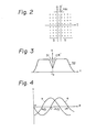
- Figure 2 is a schematic pattern view of the distribution of coded points of I-ch and Q-ch data.
- the ordinate I represents the i-ch
- the abscissa Q the Q-ch, taking the case of 64-value QAM as an example.
- the character Q' indicates the location of an axis which would be located under a conventional 64-value QAM.
- the axis Q' is, however, offset by V de to become the axis Q, because the DC offset V de of the DC offset source 108 is added to the I-ch data signal.
- Figure 3 is a graph of a spectrum of the output from the transmitter unit 100 shown in Fig. 1.
- the ordinate f indicates a frequency
- the abscissa V a voltage.
- the output from the transmitter unit 100 i.e., the modulated transmission signal
- the leakage carrier CR' stands at the middle of the spectrum. That is, the carrier component also appears in the modulated transmission signal, simultaneously.
- the signal components existing in the vicinity of the leakage carrier CR' are preferably filtered by means of the high-pass filters 105 and 106 of Fig.
- the low-pass filters 207 and 208 are inherent and conventional in this kind of radio communication system for restricting the frequency band of the data signals to be dealt with.
- the low-pass filters 205 and 260 in the receiver unit 200 are inherent and conventional in this kind of radio communication system for extracting the desired base band signal only.
- Figure 4 depicts waveforms for explaining the carrier recovery circuit 202 of Fig. 1.
- the ordinate P represents the phase and the abscissa V the voltage.
- a sine curve a and a cosine curve b respectively represent the waveforms of signals appearing at portions a and@.
- the leakage carrier is extracted by the leakage carrier extracting filter 222.
- phase control is effected by the variable phase shifter 223 to the thus extracted leakage carrier so as to attain optimum synchronous detections at the individual mixers 203 and 204.
- the thus phase-controlled carrier CR' is supplied, on one hand, to the mixer 203 directly and, on the other hand, to the mixer 204 with a phase shift of ⁇ /2 by the ⁇ /2 phase shifter 223.
- the carrier CR' is used for the I-ch and Q-ch synchronous detection operations at the mixers 203 and 204 with the modulated transmission signal received through the hybrid circuit 201, to be specific, with the two route modulated transmission signals branched, at the circuit 201, into the mixers 203 and 204.
- the waveforms of Fig. 4 specifically represent the characteristics in phase of the thus synchronously detected signals, where the optimum phase is obtained at the phase 0 of the sine curve a when the sine value indicates zero voltage. Accordingly, feedback control is given, via the low-pass filter 225 and the DC amplifier 226, to the variable phase shifter 223 in such a manner as to maintain the voltage at the portion at zero. At this time, the voltage at the portion @ becomes maximum.
- the voltage at the portion a represents an output voltage corresponding to the route signal to which the aforesaid DC offset V de is not added in the transmitter unit 100.
- the output from the mixer 204 is the base band signal.
- the base band signal necessarily contains a sine wave signal (a) having a very low frequency due to a beat signal between an inherent carrier component and the extracted leakage carrier component.
- the sine wave signal (a) is extracted by means of the low-pass filter 225 and fed back, via the amplifier 226, to the phase shifter 223 until the sine wave value (a) is made zero.
- the hardware for constructing the carrier recovery circuit 202 can be significantly simplified compared with the hardware under the prior art multiply method for demodulation. This is caused by the use of the leakage carrier derived from the DC offset. Further, it is recognized that the system of Fig. 1 is operated under the so-called absolute phase modulation method, i.e., the modulation signal having the same phase as that of the carrier is allotted to be data "0" or "00" fixedly. It is known that the absolute phase modulation method is available for decreasing a data error rate.
- FIG. 5 is a block diagram of a radio communication system according to a second embodiment of the present invention. The difference here is only that a carrier recovery circuit 221 does not contain the leakage carrier extracting filter 222 and the variable phase shifter 223, as in the related circuit 202 of the first embodiment. Therefore, the carrier recovery circuit 221 does not positively extract the leakage carrier CR', as in the corresponding circuit 202, but indirectly utilizes the leakage carrier for the synchronous detections in the mixers 203 and 204.
- the reason why the synchronous detections can be achieved without extracting the leakage carrier CR' is as follows.
- the output from the filter 114 of the transmitter unit 100 is expressed by equation (1).
- the symbol x(t) denotes a component of the I-ch data signal DI in and the symbol y(t) a component of the Q-ch data signal DQ, n .
- the coswt component and sin ⁇ t component are given at the mixers 109 and 110, respectively.
- the signal f(t) is applied, in the receiver unit 200, to the mixers 203 and 204 and demodulated with the sin(wt+8) component.
- a signal of is obtained at the portion @, which is expressed as follows.
- the first expression i.e., indicates the component of the I-ch data signal Dl out
- the second expression i.e., 1 ⁇ 2y(t)cos ⁇
- the filter 227 can also cancel the signal components of x(t) and y(t). Then only the output V dc sin ⁇ is given from the filter 227.
- the V de sin8 is a leakage component.
- the V dc sin ⁇ can be reduced to zero, i.e., ⁇ 0, when the inherent carrier component (sinwt) becomes in phase with the leakage carrier component (sin( ⁇ t+ ⁇ )).
- the output V de sin8 from the filter 227 is supplied, via an amplifier 228, to a control terminal of a voltage-controlled oscillator (VCO) 229 so as to lead the phase 8 to zero.
- VCO voltage-controlled oscillator
- the carrier recovery circuit 221 operates as a so-called phase- locked loop (PLL) circuit under control of the DC component (V dc sin ⁇ ) as such to minimize it to zero.
- the DC component is obtained from either one of the two route signals to which no DC offset is added in the transmitter unit 100.
- the carrier recovery circuit 221 has an advantage in that no leakage carrier extracting filter, such as the filter 222 of Fig. 1, is needed, which filter is usually very expensive due to high requisite quality factor (Q).
- the circuit 221 has another advantage in that the optimum synchronous detection can be maintained even though the frequency of the leakage carrier deviates slightly from nominal value, because no high Q filter is used therein.
- the V-shaped recess 31 is formed in the middle of the spectrum 32 representing the modulated transmission signal component, for the purpose of clear separation between the leakage carrier CR' and the modulated transmission signal. That is, signal components of a relatively narrow frequency band including the carrier CR' therein must be suppressed, in advance, to some extent.
- the high-pass filters 105 and 106 are introduced in the transmitter unit 100.
- the filters 105 and 106 are advantageous in view of the above-mentioned clear separation between CR' and the transmission signal, there is, conversely, a certain disadvantage in that the low frequency components of the I-ch and Q-ch data signals are largely filtered off unintentionally. This necessarily causes, in the receiver side, an increase of data error in the reproduced data signals Dl out and DQ out .
- an incompatible relationship stands in that, if a filtering frequency, i.e., a cut-off frequency, of the low frequency components is raised, the data of the transmission signal is remarkably deteriorated.
- the filtering frequency is lowered, while the data deterioration is improved, the S/N ratio of the leakage carrier CR' is deteriorated. In the latter case, i.e., the filtering frequency is lowered, a considerably complicated carrier recovery circuit may be necessary.
- the high-pass filters 207 and 208 function to increase the level of the low frequency components which are suppressed, relative to the level of the frequency components which are not suppressed, of the transmission signal.
- These low-pass filters 207 and 208 are preferably designed so that each has a transfer function H'(jw) inverse to a transfer function H(jw) of each of the high-pass filters 105 and 106.
- This relative inverse relationship will be expressed as follows. That is, assuming that stand and, at the same time, are satisfied, is obtained, where the symbols A(w) and A'(w) represent amplitude components and B( ⁇ ) and B'(w) represent phase components of the signals passing through the respective filters. It should be understood that equation (5) reveals the relative inverse characteristics between the transfer function of each low-pass filter (207, 208) and that of each high-pass filter (105, 106).
- Figure 6 is a graph of the transfer function characteristics of the filters (105, 106, 207, 208).
- the ordinate f denotes a frequency and the abscissa L an output level of the concerned filters.
- HPF high-pass filter
- LPF low-pass filter
- the output levels L of the curves HPF and LPF reach the same level of -K/2 dB at the cross-over frequency f co therebetween, when the lowest level of the curve HPF is assumed as -K dB. If such relative inverse characteristics cannot be satisfied, undesired distortion of data is inevitably created during the data reproduction in the receiver side.
- Figure 7 shows graphs of frequency spectrums of major signals appearing along the order of the signal flow from the transmitter unit 100 to the receiver unit 200.
- the ordinate V indicates a voltage level of the signal and the abscissa f a frequency thereof.
- Graph (a) represents the transmission spectrum of the data signal Dl,,, (same as DQ ⁇ n ) '
- the spectrum of graph (a) is transformed as that of graph (b) by means of the high-pass filter 105 (same as the filter 106). Thereafter, the output signal from the filter 105 is modulated at the mixer 109 (same as the mixer 110) so that the spectrum of the graph (c) is obtained at the output of the filter 114, which is substantially the same as the graph of Fig. 3.
- the transmission signal is demodulated by the mixer 203 (same as the mixer 204) to produce the spectrum of the graph (d) at the output of the filter 205 (206).
- the low-pass filter 207 (same as the filter 208)
- the level of the low frequency component suppressed before in the transmitter unit 100 is relatively increased.
- the term "relatively” means that the high frequency component side of the signal is suppressed as illustrated by the hatching area in graph (e), which relates to the output of the filter 217 (218).
- the broken line curve LPF represents a filtering characteristic of the low-pass filter.
- the signal from the filter 207 (208) is amplified to produce the spectrum of graph (f), which spectrum represents the spectrum of the reproduced base band signal.
- the amplification of the signal is achieved by the base band amplifier 209 (210).
- Figure 8 is a block diagram of a modified radio communication system, based on the first embodiment of Fig. 1, according to the present invention. Attention should be paid here that a high-pass filter 115 (corresponding to the filter 105) and a low-pass filter 217 (corresponding to the filter 207) have inverse characteristics in transfer function relative to each other, conforming to equation (5). Similarly, a high-pass filter 116 (corresponding to the filter 106) and a low-pass filter 218 (corresponding to the filter 208) have inverse characteristics in transfer function relative to each other, conforming to equation (5).
- Figure 9 illustrates a detailed example of the high-pass filter 115 (116) shown in Fig. 8.
- Figure 10 illustrates a detailed example of the low-pass filter 217 (218) shown in Fig. 8.
- symbols C indicate a capacitor, R a resistor, and L a coil. It is also possible to utilize a so-called active filter using an operational amplifier, instead of the passive filter (C, R, L).
- the above explanations with reference to Figs. 8, 9 and 10, are made relying on the first embodiment. It is matter of course, that the same explanations also apply to the second embodiment.
- the base band amplifier 209 (same as the amplifier 210) in Fig. 1 (also Fig. 5) must be fabricated, in actuality, as a multiamplifier connected in cascade. That is, although the data distortion can be improved by a combination of the high-pass filter (115, 116) and the low-pass filter (217, 218), an amplifying operation as high as several tens dB is required in the receiver unit 100, conversely.
- the level of the related signal is decreased due to the presence of the low-pass filter 217 (same as the filter 218). Therefore, it is preferable to bring an amplifying function into the process of graph (e), so that the amplifying function of graph (f) may substantially be removed from the receiver unit 200.
- the feedback amplifier be a single- stage amplifier and not a multiamplifier connected in cascade.
- Figure 11 illustrates part of a modification of the receiver unit 200 shown in Fig. 8.
- the feedback amplifier is referenced by numeral 219, instead of the combination of the members 217 and 209, and by numeral 220, instead of the members 218 and 210.
- the system with the receiver unit of Fig. 11 can minimize deterioration of data.
- FIG. 12 is a block diagram of a radio communication system shown in Fig. 1 with an ALC circuit.
- the ALC circuit is referenced by numeral 230.
- an ALC circuit is conventionally comprised of a variable gain amplifier, a filter for extracting a low frequency component from the output of the variable gain amplifier, a detector detecting the output from the filter, and a DC amplifier.
- Figure 13 illustrates an example of a conventional ALC circuit.
- the conventional members are specifically illustrated as the variable gain amplifier AMP, the detector DET, and the low-pass filter LPF.
- the ALC circuit of Fig. 13 functions as a so-called self-controlled circuit. Therefore, the ALC is performed with an average power of the received signal via the transmission line. Accordingly, it is not easy to perform a precise ALC operation.
- another ALC circuit construction can be realized with the use of the mixer 203.
- the mixer 203 operates with a function equivalent to that of the detector DET (Fig. 13) in addition to its inherent demodulation function.
- the mixers 203 and 204 achieve the synchronous detection for the carrier component CR with phase differences of 0 and n/2, respectively.
- the sine wave curve a and the cosine wave curve b are seen constantly at the portions @ and @ (Fig. 8), respectively, after completion of the synchronization with the carrier component CR.
- the synchronous detection is performed in such a manner as to trace the point of the phase 0 along the sine wave a (Fig. 4).
- the level of the cosine wave curve reached its maximum. This means that the output of the mixer 203, at the portion @ provides always a peak level of the received signal. Therefore, it is considered that the ALC function can also be performed by tracing the peak level.
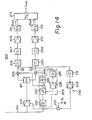
- FIG 14 is a detailed block diagram of an ALC circuit 230 in the receiver unit 200 shown in Fig. 12.
- the ALC circuit 230 is comprised of a low-pass filter 231, a DC amplifier 232, a subtractor 233, and a variable gain amplifier 234.
- the output from the mixer 203 is the base band signal.
- the base band signal necessarily contains a cosine wave signal (b) having very low frequency due to a beat signal between an inherent carrier component CR and the leakage carrier component CR'.
- the cosine wave signal (b) is extracted by means of the low-pass filter 231.
- the output from the filter 231 is DC amplified by the DC amplifier 232.
- the output from the amplifier 232 therefore varies in level in accordance with the level of the received transmission signal.
- the output level of the amplifier 232 also varies with respect to a reference gain control voltage V e .
- the variation of the received signal level can be detected as an output from the subtractor 233, which produces a level difference between the output of the amplifier 232 and the reference voltage V c .
- the amplifier 234 is gain controlled so as to achieve the ALC operation.
- the ALC circuit is applicable not only to the receiver unit 200 of the first embodiment as disclosed above, but also to that of the second embodiment.
- the present invention can provide a radio communication system operated under a multivalue QAM method, which is commercially available, even with a multivalue of 32 or higher.
Landscapes
- Engineering & Computer Science (AREA)
- Computer Networks & Wireless Communication (AREA)
- Signal Processing (AREA)
- Digital Transmission Methods That Use Modulated Carrier Waves (AREA)
Description
- The present invention relates to a radio communication system.
- In a radio communication system in which data is transmitted on a radio transmission line from a transmitter unit and the transmission data is demodulated and reproduced at a receiver unit, a carrier is digitally modulated according to data to be transmitted. A variety of methods have been proposed and put into practical use for such digital modulation. The present invention relates primarily to a quadrature amplitude modulation, QAM, radio communication system.
- In a QAM radio communication system, the carrier is modulated in phase and, at the same time, in amplitude according to data to be transmitted. The data is thereby transmitted as one of many corresponding coded points arranged on an imaginary plane. This enables a large amount of data to be transmitted at one time and thus significantly increases the transmission capacity of a radio transmission line.
- According to the QAM method, many coded points corresponding to data are created, as mentioned above. The number of coded points may be 16, 32, 64, and sometimes as much as 128 and so on. In the QAM method, one of the significant functions of the receiver unit is the recovery of a reference carrier from the transmission signal, which is used for a synchronous detection. That is, the thus recovered carrier is used to demodulate the transmission data and reproduce the original data.
- The most frequently used QAM method is the 16-value method. In this case, a process identical to a known process under a typical 4-phase phase shift keying (PSK) method is usually utilised for recovering said reference carrier. That is, the so-called multiply method, such as the two-multiply or four-multiply method, may be used for realising the process. In this case, there is further provided a phase selection control process in a reference carrier recovery circuit.
- In the higher value QAM methods, such as the 16-value methods, a problem arises, when using the prior art reference carrier recovery circuit, in suppressing so-called jitter (fluctuation) of the reference carrier. With 32- 64-, and 128-value QAM methods, recovery of a reference carrier for synchronous detection, with the use of the prior art reference carrier recovery circuit is impossible for all intents and purposes.
- In view of the above, it is desired to realise a QAM radio communication system for a multivalue QAM method of even 32-value or higher.
- According to the present invention, there is provided a quadrature amplitude modulation, QAM, radio communication system including:
- a transmitter unit operative to modulate an in-phase-channel, I-ch, data signal and quadrature- channel, Q-ch, data signal on respective carrier signals, CR, having a phase difference of n/2 with each other, to add the thus modulated carrier signals to each other, and to transmit a transmission signal to a transmission line; and
- a receiver unit operative to receive said transmission signal via said transmission line, to separate said transmission signal into both a first received signal representing said I-ch data signal and a second received signal representing said Q-ch data signal, to demodulate the first and second received signals with respective carrier signals having a phase difference of rr/2 with each other, which carrier signals are output from a carrier recovery circuit, and to reproduce original data signals from the thus demodulated signals, characterised in that
- the transmitter unit includes a direct current, DC, offset source, which is arranged to add a DC offset to one of said I-ch and Q-ch data signals, and
- the receiver unit is adapted to achieve the demodulation operation through synchronous detections of said first and second received signals by utilising a leakage carrier signal which is created due to said DC offset and included in said transmission signal, the leakage carrier signal being phase controlled and transformed into two leakage carrier signals having a phase difference of rr/2 with each other in said carrier recovery circuit, the leakage carrier signals being applied to said first and second received signals, respectively, for carrying out said synchronous detections.
- Reference is made, by way of example, to the accompanying drawings, wherein:
- Fig. 1 is a block diagram of a radio communication system according to a first embodiment of the present invention;
- Fig. 2 is a schematic pattern view of the distribution of coded points of I-ch and Q-ch data;
- Fig. 3 is a graph of a spectrum of the output from a transmitter unit shown in Fig. 1;
- Fig. 4 depicts waveforms for explaining a carrier recovery circuit of Fig. 1;
- Fig. 5 is a block diagram of a radio communication system according to a second embodiment of the present invention;
- Fig. 6 is a graph of the transfer function characteristics of the filters;
- Fig. 7 is graphs of frequency spectrums of major signals appearing along the order of the signal flow from the transmitter unit to the receiver unit;
- Fig. 8 is a block diagram of a modified radio communication system, based on the first embodiment of Fig. 1, according to the present invention;
- Fig. 9 illustrates a detailed example of a high-pass filter shown in Fig. 8;
- Fig. 10 illustrates a detailed example of low-pass filter shown in Fig. 8;
- Fig. 11 illustrates a part of a modification of a receiver unit shown in Fig. 8;
- Fig. 12 is a block diagram of a radio communication system shown in Fig. 1, to which an automatic level control (ALC) circuit is added;
- Fig. 13 illustrates an example of a conventional ALC circuit; and
- Fig. 14 is a detailed block diagram of an ALC circuit in the receiver unit shown in Fig. 12.
- Figure 1 is a block diagram of a radio communication system according to a first embodiment of the present invention. In Fig. 1,
reference numeral 100 represents a transmitter unit, 200 a receiver unit, and 150 a transmission (radio wave) line connecting the two. A transmission data signal DIn coded by, for example, pulse code modulation (PCM) is supplied to an input stage of thetransmitter unit 100 and then transformed, via a serial/ parallel converter (S/P) 101, into a parallel data signal. The parallel data signal is further transformed, via a digital/analog converter (D/A) 102, into an analog data signal. Furthermore, taking as an example a 64-value QAM, the analog data signal is divided into two route signals each composed of 3-bit signals. Thus, two route analog signals DIIN and DQin are produced therefrom, each expressing 8 (=23) values of data. The signal DIin is the so-called in-phase (I)-channel (ch) data signal. The signal DQin is the so-called quadrature (Q)-ch data signal. The I-ch data signal DIin and the Q-ch data signal DQ,n are transferred to a hybrid circuit (H) 112 by way of low-pass filters pass filters adder 107. - The
adder 107 and a direct current (DC)offset source 108 cooperating therewith are new members never before seen in prior art systems. A DC offset Vdc is given to either one of the quadrature signals (DIin, DQin). The signals from theadder 107 and thefilter 106 are applied tomixers mixer 110 directly and, on the other hand, to themixer 109, via a rr/2 phase shifter (rr/2) 111. Thus, a modulation operation is performed by each of themixers hybrid circuit 112. The added signal is then amplified by anintermediate frequency amplifier 113, and the desired frequency band component of the signal is extracted by a band-pass filter 114. The thus filtered signal is then amplified up to a predetermined transmission level by means of a high power transmission amplifier (not shown). The amplified signal is transmitted, via thetransmission line 150, to thereceiver unit 200. - At the
receiver unit 200, the transmitted signal is received and then divided by ahybrid circuit 201 into two route signals. The two route signals are demodulated bymixers carrier recovery circuit 202. Thecarrier recovery circuit 202 is also a new member never before seen in prior art systems and is closely related in operation particularly with theDC offset source 108 in thetransmitter unit 100. The thus demodulated two route receiving signals are transferred to individual analog/digital converters (A/D) 211 and 212, via low-pass filters pass filters base band amplifiers converters - The
carrier recovery circuit 202, mentioned earlier, is mainly comprised of, for example, a leakagecarrier extracting filter 222, avariable phase shifter 223, a π/2phase shifter 224, a low-pass filter 225, and aDC amplifier 226. Thecircuit 202 and also theDC offset source 108 are, as previously mentioned, new. These two elements will be explained in detail immediately below. - Figure 2 is a schematic pattern view of the distribution of coded points of I-ch and Q-ch data. In Fig. 2, the ordinate I represents the i-ch, and the abscissa Q the Q-ch, taking the case of 64-value QAM as an example. The character Q' indicates the location of an axis which would be located under a conventional 64-value QAM. The axis Q' is, however, offset by Vde to become the axis Q, because the DC offset Vde of the DC offset
source 108 is added to the I-ch data signal. - Usually, signal components defined by the coded points of a right side phase with respect to a central axis Q' and signal components defined by the coded points of the left side phase would occur with almost the same probability, because coded points of 64 values generally occur quite randomly. As a result, there is generally no possibility that the carrier component will be in only one particular direction when the coded points occur randomly in the plane defined by both the axis Q' and the axis I.
- On the other hand, if the offset V de is forcibly added to the I-ch data signal so as to shift the usual axis Q' to the axis Q, along with present invention, the signal components of the right side phase, with respect to the center axis Q, and the signal components of the left side phase occur at an unbalanced ratio of 5:3, as shown in Fig. 2. Therefore, a relative surplus level of 2(=5-3) is provided, and the aforesaid leakage carrier can always be obtained. As a result, a carrier can always stand in the modulated transmission signal.
- Figure 3 is a graph of a spectrum of the output from the
transmitter unit 100 shown in Fig. 1. The ordinate f indicates a frequency, and the abscissa V a voltage. Usually, the output from thetransmitter unit 100, i.e., the modulated transmission signal, exhibits a flat characteristic at the middle of the spectrum, as illustrated by the broken line in the graph. Therefore, no carrier can be observed. If, however, the DC offset Vde is added to the data signal, the leakage carrier CR' stands at the middle of the spectrum. That is, the carrier component also appears in the modulated transmission signal, simultaneously. In this case, the signal components existing in the vicinity of the leakage carrier CR' are preferably filtered by means of the high-pass filters recess 31 of the spectrum) in order to easily pick up the leakage carrier CR'. The thus filtered signal components are recovered, in thereceiver unit 200, by the low-pass filters pass filters transmitter unit 100 are inherent and conventional in this kind of radio communication system for restricting the frequency band of the data signals to be dealt with. Also, the low-pass filters 205 and 260 in thereceiver unit 200 are inherent and conventional in this kind of radio communication system for extracting the desired base band signal only. - Figure 4 depicts waveforms for explaining the
carrier recovery circuit 202 of Fig. 1. In the graph, the ordinate P represents the phase and the abscissa V the voltage. A sine curve a and a cosine curve b respectively represent the waveforms of signals appearing at portions ⓐ and@. - Returning to Fig. 1 again, the leakage carrier is extracted by the leakage
carrier extracting filter 222. Then, phase control is effected by thevariable phase shifter 223 to the thus extracted leakage carrier so as to attain optimum synchronous detections at theindividual mixers mixer 203 directly and, on the other hand, to themixer 204 with a phase shift of π/2 by the π/2phase shifter 223. Thus, the carrier CR' is used for the I-ch and Q-ch synchronous detection operations at themixers hybrid circuit 201, to be specific, with the two route modulated transmission signals branched, at thecircuit 201, into themixers pass filter 225 and theDC amplifier 226, to thevariable phase shifter 223 in such a manner as to maintain the voltage at the portion at zero. At this time, the voltage at the portion @ becomes maximum. The voltage at the portion ⓐ represents an output voltage corresponding to the route signal to which the aforesaid DC offset Vde is not added in thetransmitter unit 100. - The output from the
mixer 204 is the base band signal. However, the base band signal necessarily contains a sine wave signal (a) having a very low frequency due to a beat signal between an inherent carrier component and the extracted leakage carrier component. The sine wave signal (a) is extracted by means of the low-pass filter 225 and fed back, via theamplifier 226, to thephase shifter 223 until the sine wave value (a) is made zero. - As explained above, the hardware for constructing the
carrier recovery circuit 202 can be significantly simplified compared with the hardware under the prior art multiply method for demodulation. This is caused by the use of the leakage carrier derived from the DC offset. Further, it is recognized that the system of Fig. 1 is operated under the so-called absolute phase modulation method, i.e., the modulation signal having the same phase as that of the carrier is allotted to be data "0" or "00" fixedly. It is known that the absolute phase modulation method is available for decreasing a data error rate. - Another arrangement instead of the
carrier recovery circuit 202 can also be used for thereceiver unit 200. Figure 5 is a block diagram of a radio communication system according to a second embodiment of the present invention. The difference here is only that acarrier recovery circuit 221 does not contain the leakagecarrier extracting filter 222 and thevariable phase shifter 223, as in therelated circuit 202 of the first embodiment. Therefore, thecarrier recovery circuit 221 does not positively extract the leakage carrier CR', as in thecorresponding circuit 202, but indirectly utilizes the leakage carrier for the synchronous detections in themixers - The reason why the synchronous detections can be achieved without extracting the leakage carrier CR' is as follows. The output from the
filter 114 of thetransmitter unit 100 is expressed by equation (1).
mixers receiver unit 200, to themixers 

symbol 8 denotes a phase difference between the inherent carrier component and the leakage carrier component. The signal components of 2wt in equation (2) are cancelled by a low-pass filter 227. Therefore, the signal f(t)sin(ωt+θ) is transformed to be
- The first expression, i.e.,

filter 227 can also cancel the signal components of x(t) and y(t). Then only the output Vdcsinθ is given from thefilter 227. The Vdesin8 is a leakage component. The Vdcsinθ can be reduced to zero, i.e., θ→0, when the inherent carrier component (sinwt) becomes in phase with the leakage carrier component (sin(ωt+θ)). Accordingly, the output Vde sin8 from thefilter 227 is supplied, via anamplifier 228, to a control terminal of a voltage-controlled oscillator (VCO) 229 so as to lead thephase 8 to zero. The oscillation frequency of theoscillator 229 is adjusted, in advance, to be optimum frequency when Vdcsinθ=0 stands. Thus, thecarrier recovery circuit 221 operates as a so-called phase- locked loop (PLL) circuit under control of the DC component (Vdcsinθ) as such to minimize it to zero. - It should be noted that the DC component is obtained from either one of the two route signals to which no DC offset is added in the
transmitter unit 100. Further, thecarrier recovery circuit 221 has an advantage in that no leakage carrier extracting filter, such as thefilter 222 of Fig. 1, is needed, which filter is usually very expensive due to high requisite quality factor (Q). Furthermore, thecircuit 221 has another advantage in that the optimum synchronous detection can be maintained even though the frequency of the leakage carrier deviates slightly from nominal value, because no high Q filter is used therein. - Referring to Fig. 3 again, the V-shaped
recess 31 is formed in the middle of thespectrum 32 representing the modulated transmission signal component, for the purpose of clear separation between the leakage carrier CR' and the modulated transmission signal. That is, signal components of a relatively narrow frequency band including the carrier CR' therein must be suppressed, in advance, to some extent. For this, in Figs. 1 and 5, the high-pass filters transmitter unit 100. - However, although the
filters - It should be recognized that, in the
receiver unit 200, the high-pass filters 207 and 208 (Figs. 1 and 5) function to increase the level of the low frequency components which are suppressed, relative to the level of the frequency components which are not suppressed, of the transmission signal. These low-pass filters pass filters 


- Figure 6 is a graph of the transfer function characteristics of the filters (105, 106, 207, 208). The ordinate f denotes a frequency and the abscissa L an output level of the concerned filters. The symbol, HPF (high-pass filter) represents the transfer function curve of each of the high-
pass filters transmitter unit 100, and LPF (low-pass filter) represents the transfer function curve of each of the low-pass filters receiver unit 200. Since the relative inverse characteristics exist, regarding the transfer functions, the output levels L of the curves HPF and LPF reach the same level of -K/2 dB at the cross-over frequency fco therebetween, when the lowest level of the curve HPF is assumed as -K dB. If such relative inverse characteristics cannot be satisfied, undesired distortion of data is inevitably created during the data reproduction in the receiver side. - Figure 7 shows graphs of frequency spectrums of major signals appearing along the order of the signal flow from the
transmitter unit 100 to thereceiver unit 200. In each graph, the ordinate V indicates a voltage level of the signal and the abscissa f a frequency thereof. Graph (a) represents the transmission spectrum of the data signal Dl,,, (same as DQ¡n)' The spectrum of graph (a) is transformed as that of graph (b) by means of the high-pass filter 105 (same as the filter 106). Thereafter, the output signal from thefilter 105 is modulated at the mixer 109 (same as the mixer 110) so that the spectrum of the graph (c) is obtained at the output of thefilter 114, which is substantially the same as the graph of Fig. 3. In thereceiver unit 200, the transmission signal is demodulated by the mixer 203 (same as the mixer 204) to produce the spectrum of the graph (d) at the output of the filter 205 (206). Further, in the low-pass filter 207 (same as the filter 208), the level of the low frequency component suppressed before in thetransmitter unit 100 is relatively increased. The term "relatively" means that the high frequency component side of the signal is suppressed as illustrated by the hatching area in graph (e), which relates to the output of the filter 217 (218). The broken line curve LPF represents a filtering characteristic of the low-pass filter. Finally, the signal from the filter 207 (208) is amplified to produce the spectrum of graph (f), which spectrum represents the spectrum of the reproduced base band signal. The amplification of the signal is achieved by the base band amplifier 209 (210). - Figure 8 is a block diagram of a modified radio communication system, based on the first embodiment of Fig. 1, according to the present invention. Attention should be paid here that a high-pass filter 115 (corresponding to the filter 105) and a low-pass filter 217 (corresponding to the filter 207) have inverse characteristics in transfer function relative to each other, conforming to equation (5). Similarly, a high-pass filter 116 (corresponding to the filter 106) and a low-pass filter 218 (corresponding to the filter 208) have inverse characteristics in transfer function relative to each other, conforming to equation (5).
- Figure 9 illustrates a detailed example of the high-pass filter 115 (116) shown in Fig. 8. Figure 10 illustrates a detailed example of the low-pass filter 217 (218) shown in Fig. 8. In both figures, symbols C indicate a capacitor, R a resistor, and L a coil. It is also possible to utilize a so-called active filter using an operational amplifier, instead of the passive filter (C, R, L). The above explanations with reference to Figs. 8, 9 and 10, are made relying on the first embodiment. It is matter of course, that the same explanations also apply to the second embodiment.
- Returning to Fig. 7 again, especially referring to the change from graph (e) to (f), it is required for the related signal to be amplified as high as, for example, several tens dB. For this, the base band amplifier 209 (same as the amplifier 210) in Fig. 1 (also Fig. 5) must be fabricated, in actuality, as a multiamplifier connected in cascade. That is, although the data distortion can be improved by a combination of the high-pass filter (115, 116) and the low-pass filter (217, 218), an amplifying operation as high as several tens dB is required in the
receiver unit 100, conversely. Referring again to the change from graph (d) to (e), it is apparent that the level of the related signal is decreased due to the presence of the low-pass filter 217 (same as the filter 218). Therefore, it is preferable to bring an amplifying function into the process of graph (e), so that the amplifying function of graph (f) may substantially be removed from thereceiver unit 200. To be specific, it is preferable to employ a feedback amplifier which both has a low-pass filtering function and exhibits an inverse characteristic relative to the characteristic by the high-pass filter 115 (116), thereby allowing the low-pass fitter 217 (218) to be substantially eliminated from thereceiver unit 200. In this case, it is sufficient that the feedback amplifier be a single- stage amplifier and not a multiamplifier connected in cascade. - Figure 11 illustrates part of a modification of the
receiver unit 200 shown in Fig. 8. The feedback amplifier is referenced bynumeral 219, instead of the combination of themembers numeral 220, instead of themembers - Finally, automatic level control (ALC), i.e., so-called AGC, will be mentioned below. ALC is usually introduced in an input stage of a receiver unit. ALC is especially important for the receiver unit, particularly the receiver unit connected to a transmission line having considerably poor transmission quality. Figure 12 is a block diagram of a radio communication system shown in Fig. 1 with an ALC circuit. The ALC circuit is referenced by
numeral 230. In the prior art, an ALC circuit is conventionally comprised of a variable gain amplifier, a filter for extracting a low frequency component from the output of the variable gain amplifier, a detector detecting the output from the filter, and a DC amplifier. Figure 13 illustrates an example of a conventional ALC circuit. The conventional members are specifically illustrated as the variable gain amplifier AMP, the detector DET, and the low-pass filter LPF. The ALC circuit of Fig. 13 functions as a so-called self-controlled circuit. Therefore, the ALC is performed with an average power of the received signal via the transmission line. Accordingly, it is not easy to perform a precise ALC operation. In the system of the present invention, another ALC circuit construction can be realized with the use of themixer 203. Themixer 203 operates with a function equivalent to that of the detector DET (Fig. 13) in addition to its inherent demodulation function. Themixers mixer 203, at the portion @ provides always a peak level of the received signal. Therefore, it is considered that the ALC function can also be performed by tracing the peak level. - Figure 14 is a detailed block diagram of an
ALC circuit 230 in thereceiver unit 200 shown in Fig. 12. As seen from Fig. 14, theALC circuit 230 is comprised of a low-pass filter 231, aDC amplifier 232, asubtractor 233, and avariable gain amplifier 234. The output from themixer 203 is the base band signal. However, the base band signal necessarily contains a cosine wave signal (b) having very low frequency due to a beat signal between an inherent carrier component CR and the leakage carrier component CR'. The cosine wave signal (b) is extracted by means of the low-pass filter 231. The output from thefilter 231 is DC amplified by theDC amplifier 232. The output from theamplifier 232 therefore varies in level in accordance with the level of the received transmission signal. At the same time, the output level of theamplifier 232 also varies with respect to a reference gain control voltage Ve. Accordingly, the variation of the received signal level can be detected as an output from thesubtractor 233, which produces a level difference between the output of theamplifier 232 and the reference voltage Vc. Based on the thus detected level variation, theamplifier 234 is gain controlled so as to achieve the ALC operation. The ALC circuit is applicable not only to thereceiver unit 200 of the first embodiment as disclosed above, but also to that of the second embodiment. - As explained above in detail, the present invention can provide a radio communication system operated under a multivalue QAM method, which is commercially available, even with a multivalue of 32 or higher.
Claims (11)
Applications Claiming Priority (6)
| Application Number | Priority Date | Filing Date | Title |
|---|---|---|---|
| JP57231634A JPS59123346A (en) | 1982-12-29 | 1982-12-29 | Radio communication system |
| JP57231635A JPS59123347A (en) | 1982-12-29 | 1982-12-29 | Radio communication system |
| JP231634/82 | 1982-12-29 | ||
| JP231636/82 | 1982-12-29 | ||
| JP57231636A JPS59123348A (en) | 1982-12-29 | 1982-12-29 | Radio communication system |
| JP231635/82 | 1982-12-29 |
Publications (3)
| Publication Number | Publication Date |
|---|---|
| EP0113246A2 EP0113246A2 (en) | 1984-07-11 |
| EP0113246A3 EP0113246A3 (en) | 1986-08-13 |
| EP0113246B1 true EP0113246B1 (en) | 1989-03-01 |
Family
ID=27331786
Family Applications (1)
| Application Number | Title | Priority Date | Filing Date |
|---|---|---|---|
| EP83307949A Expired EP0113246B1 (en) | 1982-12-29 | 1983-12-23 | Radio communication system |
Country Status (5)
| Country | Link |
|---|---|
| US (1) | US4581748A (en) |
| EP (1) | EP0113246B1 (en) |
| KR (1) | KR860002217B1 (en) |
| CA (1) | CA1217233A (en) |
| DE (1) | DE3379311D1 (en) |
Families Citing this family (15)
| Publication number | Priority date | Publication date | Assignee | Title |
|---|---|---|---|---|
| JPH0714170B2 (en) * | 1983-11-30 | 1995-02-15 | 富士通株式会社 | Carrier wave regeneration circuit |
| US4638504A (en) * | 1985-06-28 | 1987-01-20 | Broadcast Electronics, Inc. | Independent channel modulation system for AM stereo |
| JPS62142440A (en) * | 1985-12-17 | 1987-06-25 | Fujitsu Ltd | Modulator-demodulator |
| US4816783A (en) * | 1988-01-11 | 1989-03-28 | Motorola, Inc. | Method and apparatus for quadrature modulation |
| JPH0481054A (en) * | 1990-06-01 | 1992-03-13 | Nec Corp | Data transmission system |
| EP0486667A4 (en) * | 1990-06-12 | 1993-08-11 | Motorola, Inc. | Communication signal having a time domain pilot component |
| US5519730A (en) * | 1990-06-12 | 1996-05-21 | Jasper; Steven C. | Communication signal having a time domain pilot component |
| SE468616B (en) * | 1991-06-12 | 1993-02-15 | Ericsson Telefon Ab L M | PROCEDURE FOR COMPENSATION OF THE TRANSMITTER USE SIGNAL'S DEPENDENCE OF THE TRANSFER FUNCTION FOR A COMBINER FILTER |
| DE4420377C2 (en) * | 1993-09-22 | 1998-08-27 | Hewlett Packard Co | Method for generating quadrature signals |
| US5751114A (en) * | 1996-05-24 | 1998-05-12 | International Business Machines Corporation | Apparatus, method and article of manufacture for carrier frequency compensation in a FM radio transmitter |
| WO1998039885A2 (en) * | 1997-03-03 | 1998-09-11 | Int Labs, Inc. | Technique to phase lock a transceiving, transmitting, or receiving local oscillator to an incoming carrier signal |
| US6252910B1 (en) * | 1998-11-11 | 2001-06-26 | Comspace Corporation | Bandwidth efficient QAM on a TDM-FDM system for wireless communications |
| GB2389019B (en) * | 2002-05-22 | 2005-10-19 | Tandberg Television Ltd | Carrier generation and recovery for higher order modulation system |
| US7062228B2 (en) * | 2004-05-10 | 2006-06-13 | Harris Corporation | Cellular communications system using baseband carrier injection and related methods |
| US7622987B1 (en) | 2007-01-25 | 2009-11-24 | Pmc-Sierra, Inc. | Pattern-based DC offset correction |
Family Cites Families (7)
| Publication number | Priority date | Publication date | Assignee | Title |
|---|---|---|---|---|
| NL122464C (en) * | 1962-02-19 | |||
| NL281180A (en) * | 1962-07-19 | |||
| NL294442A (en) * | 1963-06-21 | |||
| BE766847A (en) * | 1971-05-07 | 1971-11-08 | Acec | PROCESS FOR TRANSMISSION OF INFORMATION WITH AUTOMATIC RESTITUTION OF THE CARRIER WAVE IN THE RECEIVER, |
| US3813598A (en) * | 1971-08-16 | 1974-05-28 | Rexon Electronics Inc | Single tone carrier recovery system |
| US3849730A (en) * | 1973-06-20 | 1974-11-19 | Bell Telephone Labor Inc | Carrier recovery in vestigial sideband data receivers |
| US4074199A (en) * | 1974-09-16 | 1978-02-14 | U.S. Philips Corporation | Vestigial-sideband transmission system for synchronous data signals |
-
1983
- 1983-12-19 CA CA000443641A patent/CA1217233A/en not_active Expired
- 1983-12-23 EP EP83307949A patent/EP0113246B1/en not_active Expired
- 1983-12-23 DE DE8383307949T patent/DE3379311D1/en not_active Expired
- 1983-12-28 KR KR1019830006248A patent/KR860002217B1/en not_active Expired
- 1983-12-28 US US06/566,401 patent/US4581748A/en not_active Expired - Lifetime
Also Published As
| Publication number | Publication date |
|---|---|
| US4581748A (en) | 1986-04-08 |
| EP0113246A2 (en) | 1984-07-11 |
| KR860002217B1 (en) | 1986-12-31 |
| DE3379311D1 (en) | 1989-04-06 |
| KR840007342A (en) | 1984-12-06 |
| EP0113246A3 (en) | 1986-08-13 |
| CA1217233A (en) | 1987-01-27 |
Similar Documents
| Publication | Publication Date | Title |
|---|---|---|
| EP0113246B1 (en) | Radio communication system | |
| FI80175C (en) | Digital telecommunication system where quadrature modulated carrier signals are used | |
| US4359692A (en) | Rapid acquisition shift keyed signal demodulator | |
| US5802451A (en) | Non-linear compensation circuit for a power amplifier | |
| US3984778A (en) | Carrier recovery scheme for a SSB-SC signal | |
| US4660193A (en) | Digital modulation method for standard broadcast FM subcarrier | |
| JPH024183B2 (en) | ||
| US4633484A (en) | Receiver unit in radio communication system | |
| EP0059415A1 (en) | System for demodulation of phase-shift keying signals | |
| US4799238A (en) | Differential phase shift keying method for the transmission of data | |
| US6707863B1 (en) | Baseband signal carrier recovery of a suppressed carrier modulation signal | |
| EP0173362B1 (en) | Arrangement of recovering a clock signal form an angle-modulated carrier signal having a modulation index m = 0.5 | |
| EP0122127B1 (en) | Radio communication system | |
| JPH0724409B2 (en) | Key level control circuit for 4-phase PSK demodulator | |
| JP2975390B2 (en) | Multi-level variable modulator / demodulator | |
| US3939407A (en) | Plural channel communications system | |
| JPH0685860A (en) | Psk demodulator | |
| EP0098665A2 (en) | Data demodulator for a direct frequency modulated signal | |
| JPH0474905B2 (en) | ||
| US5878084A (en) | Method and apparatus for recovering the independent bit streams from each of two co-channel frequency modulated carriers | |
| JP2545882B2 (en) | Data playback device | |
| KR19980015798A (en) | Carrier recovery apparatus of quadrature phase shift demodulator | |
| JP2874450B2 (en) | Demodulator | |
| JPH03133236A (en) | Demodulator | |
| JPH0211047A (en) | Carrier regeneration circuit |
Legal Events
| Date | Code | Title | Description |
|---|---|---|---|
| PUAI | Public reference made under article 153(3) epc to a published international application that has entered the european phase |
Free format text: ORIGINAL CODE: 0009012 |
|
| AK | Designated contracting states |
Designated state(s): DE FR GB IT NL SE |
|
| PUAL | Search report despatched |
Free format text: ORIGINAL CODE: 0009013 |
|
| AK | Designated contracting states |
Kind code of ref document: A3 Designated state(s): DE FR GB IT NL SE |
|
| 17P | Request for examination filed |
Effective date: 19861003 |
|
| 17Q | First examination report despatched |
Effective date: 19871020 |
|
| GRAA | (expected) grant |
Free format text: ORIGINAL CODE: 0009210 |
|
| AK | Designated contracting states |
Kind code of ref document: B1 Designated state(s): DE FR GB IT NL SE |
|
| REF | Corresponds to: |
Ref document number: 3379311 Country of ref document: DE Date of ref document: 19890406 |
|
| ITF | It: translation for a ep patent filed | ||
| ET | Fr: translation filed | ||
| PLBE | No opposition filed within time limit |
Free format text: ORIGINAL CODE: 0009261 |
|
| STAA | Information on the status of an ep patent application or granted ep patent |
Free format text: STATUS: NO OPPOSITION FILED WITHIN TIME LIMIT |
|
| 26N | No opposition filed | ||
| ITTA | It: last paid annual fee | ||
| PGFP | Annual fee paid to national office [announced via postgrant information from national office to epo] |
Ref country code: GB Payment date: 19921013 Year of fee payment: 10 |
|
| PGFP | Annual fee paid to national office [announced via postgrant information from national office to epo] |
Ref country code: SE Payment date: 19921111 Year of fee payment: 10 |
|
| PGFP | Annual fee paid to national office [announced via postgrant information from national office to epo] |
Ref country code: FR Payment date: 19921221 Year of fee payment: 10 |
|
| PGFP | Annual fee paid to national office [announced via postgrant information from national office to epo] |
Ref country code: NL Payment date: 19921231 Year of fee payment: 10 |
|
| PGFP | Annual fee paid to national office [announced via postgrant information from national office to epo] |
Ref country code: DE Payment date: 19930226 Year of fee payment: 10 |
|
| PG25 | Lapsed in a contracting state [announced via postgrant information from national office to epo] |
Ref country code: GB Effective date: 19931223 |
|
| PG25 | Lapsed in a contracting state [announced via postgrant information from national office to epo] |
Ref country code: SE Effective date: 19931224 |
|
| PG25 | Lapsed in a contracting state [announced via postgrant information from national office to epo] |
Ref country code: NL Effective date: 19940701 |
|
| NLV4 | Nl: lapsed or anulled due to non-payment of the annual fee | ||
| GBPC | Gb: european patent ceased through non-payment of renewal fee |
Effective date: 19931223 |
|
| PG25 | Lapsed in a contracting state [announced via postgrant information from national office to epo] |
Ref country code: FR Effective date: 19940831 |
|
| PG25 | Lapsed in a contracting state [announced via postgrant information from national office to epo] |
Ref country code: DE Effective date: 19940901 |
|
| REG | Reference to a national code |
Ref country code: FR Ref legal event code: ST |
|
| EUG | Se: european patent has lapsed |
Ref document number: 83307949.4 Effective date: 19940710 |