EP0113334A2 - Im Normalstand abgeschaltete Halbleiteranordnung mit niedrigem Betriebswiderstand und analoge Schaltung - Google Patents
Im Normalstand abgeschaltete Halbleiteranordnung mit niedrigem Betriebswiderstand und analoge Schaltung Download PDFInfo
- Publication number
- EP0113334A2 EP0113334A2 EP84100025A EP84100025A EP0113334A2 EP 0113334 A2 EP0113334 A2 EP 0113334A2 EP 84100025 A EP84100025 A EP 84100025A EP 84100025 A EP84100025 A EP 84100025A EP 0113334 A2 EP0113334 A2 EP 0113334A2
- Authority
- EP
- European Patent Office
- Prior art keywords
- region
- gate
- layer
- electrode
- emitter
- Prior art date
- Legal status (The legal status is an assumption and is not a legal conclusion. Google has not performed a legal analysis and makes no representation as to the accuracy of the status listed.)
- Withdrawn
Links
Images
Classifications
-
- H—ELECTRICITY
- H03—ELECTRONIC CIRCUITRY
- H03K—PULSE TECHNIQUE
- H03K17/00—Electronic switching or gating, i.e. not by contact-making and –breaking
- H03K17/51—Electronic switching or gating, i.e. not by contact-making and –breaking characterised by the components used
- H03K17/56—Electronic switching or gating, i.e. not by contact-making and –breaking characterised by the components used by the use, as active elements, of semiconductor devices
- H03K17/567—Circuits characterised by the use of more than one type of semiconductor device, e.g. BIMOS, composite devices such as IGBT
-
- H—ELECTRICITY
- H10—SEMICONDUCTOR DEVICES; ELECTRIC SOLID-STATE DEVICES NOT OTHERWISE PROVIDED FOR
- H10D—INORGANIC ELECTRIC SEMICONDUCTOR DEVICES
- H10D84/00—Integrated devices formed in or on semiconductor substrates that comprise only semiconducting layers, e.g. on Si wafers or on GaAs-on-Si wafers
- H10D84/40—Integrated devices formed in or on semiconductor substrates that comprise only semiconducting layers, e.g. on Si wafers or on GaAs-on-Si wafers characterised by the integration of at least one component covered by groups H10D12/00 or H10D30/00 with at least one component covered by groups H10D10/00 or H10D18/00, e.g. integration of IGFETs with BJTs
- H10D84/401—Combinations of FETs or IGBTs with BJTs
- H10D84/403—Combinations of FETs or IGBTs with BJTs and with one or more of diodes, resistors or capacitors
- H10D84/409—Combinations of FETs or IGBTs with lateral BJTs and with one or more of diodes, resistors or capacitors
Definitions
- the present invention relates to a normally-off semiconductor device with low on-resistance and to a circuit analog of such device.
- a junction field-effect transistor(hereinafter designated 'JFET) of the N-channel type typically comprises a channel region of N-type semiconductor material and a P-type gate region adjoining the N-type channel region and forming a P-N junction therewith.
- a depletion region is formed in the vicinity of the P-N junction and extends into the N-type channel region so as to shrink the portion of the channel that can conduct current.
- the JFET is in, what is known in the art as, a pinched-off condition in which it cannot conduct current.
- a JFET is a normally-on device; that is, a JFET's gate region must be biased in order to pinch off the JFET. In many applications, however, it is desirable to have normally-off device operation. Such normally-off operation is achieved in an electrical circuit described and claimed in the above- referenced application. In such circuit, a JFET is serially connected to a bipolar transistor, with the base elecrode of the bipolar transistor serving as a gate or control electrode for the circuit. Normally-off operation of the JFET is achieved because the base electrode must be appropriately biased to turn on the bipolar transistor and allow the JFET to conduct current.
- the gate of the JFET is electrically shorted to the emitter of the bipolar transistor, resulting in the P-N junction of the JFET being reverse-biased, at least to a slight extent, while the JFET is conducting current.
- the circuit cannot take advantage of a technique for markedly lowering the on-resistance of a JFET, which involves forward-biasing the P-N junction of the JFET. With the P-N junction sufficiently forward-biased, the P-type gate region injects holes into the N-type channel, resulting in a lowering of the channel resistance, and hence, lowering of the on-resistance of the JFET.
- a further object of my invention is to provide an electrical circuit including a JFET that operates in a normally-off fashion with reduced on-resistance, wherein the circuit advantageously requires only a single control signal.
- Another object of my invention is to provide a semiconductor device of compact size, including a normally-off JFET with reduced on-resistance.
- I provide a semiconductor device including an N-channel region, a P-gate region forming a P-N junction with the N-channel region, and a bipolar transistor for achieving normally-off operation.
- the bipolar transistor is formed integrally with the P-gate region and includes N + (or highly-doped) emitter and collector regions adjoining the P-gate region.
- the P-gate region in the vincinity of the emitter and collector regions, functions as the P-base region of the bipolar transistor.
- the portion of the P-gate region situated between the P-base region and a P gate contact region which adjoins the P-gate region provides electrical resistance between the P-base region and the P gate contact region.
- a single gate electrode adjoining the P gate contact region serves as a control electrode for the entire device.
- the collector region is ohmically connected to the source side of the N-channel region.
- the P-N junction between the P-gate region and the N-channel region is forward biased when the bipolar transistor is biased into conduction, so that the device on-resistance (i.e., JFET on-resistance plus bipolar transistor on-resistance) is low.
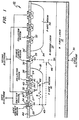
- FIG. 1 a cross section of a preferred cell, or repeated structure, of a semiconductor device 10 in accordance with my invention. Only the left-hand side of the illustrated cell of device 10 is described in detail herein, inasmuch as the right-hand side thereof is preferably symmetrical to the left-hand side, as illustrated.
- Device 10 includes a first layer 12, which is highly-doped with N-type impurities, designated "N + " in the art, and preferably comprises a bulk substrate.
- gate region 16 Adjoining the upper portion of the second layer 14 is gate region 16, doped with P-type impurities to a reference level, designated "P", and preferably formed by diffusion or ion implantation.
- P P-type impurities
- a P-N junction 18 exists between P gate region 16 and N - second layer 14.
- P-gate region 16 Adjoining the upper portion of P-gate region 16 are each of three regions: a P (or highly doped P-type) gate contact region 20, an N emitter region 22, and an N collector region 24.
- a P-N junction 26 exists between N + collector region 24 and P gate region 16, and a further P-N junction 27 exists between N emitter region 22 and P gate region 16.
- N + source contact region 28 also adjoins the upper portion of N - second layer 14.
- Device 10 advantageously is a three-electrode device, comprising a first electrode 30 adjoining the underside of N + substrate layer 12, a second electrode 32 adjoining N emitter region 22. and a gate electrode 34 adjoining P gate contact region 20. Additionally, an interconnection electrode 36 ohmically connects together N + collector region 24 and N + source contact region 28. Interconnection electrode 36 suitably comprises metallization adjoining both regions 24 and 28 and is preferably separated dielectrically from N - second layer 14 and P gate region 16 by an insulating layer 38, atop the device. Layer 38 suitably comprises, for example, silicon dioxide or silicon nitride. Further insulation layers 40, 42 and 44 respectively, perform similar dielectric separation functions between each of electrodes 36, 32 and 34 and P gate region 16.
- Insulation layers 38, 40, 42, and 44 formed in conventional fashion, additionally are useful as diffusion masks during the formation of the small regions at the upper portion of device 10: i.e., regions 20, 22, 24, and 28.
- the separation of the various electrodes on the upper surface of device 10, for example, 32 and 34, is suitably accomplished with photolithographic technique.
- an inherent, N-channel junction field-effect transistor (JFET) 46 in device 10 is formed from N + first layer 12, constituting a drain, designed D ; N + source contact region 28, constituting a source, designated S; and P gate region 16, constituting a gate, designated G.
- an N-P-N bipolar transistor 48 formed from N + collector region 24, designated C; N + emitter region 22, designated E; and the portion of P gate region 16 in the vicinity of emitter and collector regions 22 and 24, respectively, designated B.
- Base B of transistor 48 is connected to gate G of JFET 46 via the inherent resistance R, existing between base B and p+ gate contact region 20,the value of which increases with increasing separation of base B from P gate contact region 20.
- No-inherent resistance is shown between gate G and location 45 of P-N junction 18 directly beneath region 20, however, inasmuch as these points are extremely close together in a practical device, much more so than is illustrated in the schematic view of Fig. 1.
- Semiconductor device 10 incorporates inherent JFET 46, inherent bipolar transistor 48, and inherent resistance R in a compact semiconductor device.
- N + collector region 24 be interposed between N + emitter region 22 and N + source contact region 28.
- device 10 can be simple of construction if a cell of semiconductor device 10 includes a second.P gate region 50, adjoining the upper portion of N - second layer 14, with the right-hand side of device 10 including P gate region 50, as illustrated, being symmetrical to the illustrated left-hand side of device 10.
- device 10 In operation of semiconductor device 10, with gate electrode 34 shorted to second electrode 32, through a low resistance conductive path (not shown), device 10 cannot conduct "forward" current (that is, positive current from first electrode 30 to second electrode 32, with second electrode 32 more positive in potential than first electrode 30). Accordingly, device 10 operates in a normally-off fashion. This occurs because,with gate electrode 34 so shorted, P-N junction 18 is reverse biased and P-N junction 27 is shorted. Inasmuch as P-N junction 27 constitutes the base-to-emitter junction of bipolar transistor 48, this prevents such transistor from turning on and conducting current that would otherwise flow from N + source contact region 28 to N + collector region 24, via interconnection electrode 36.
- device 10 can conduct "reverse" current (that is, positive current from second electrode 32 to first electrode 30, with second electrode 32 sufficiently more positive in potential than first electrode 30). This is because a current path then exists through device 10 from second electrode 32, through shorted gate electrode 34, P gate contact region 20, P gate region 16, P-N junction 18 (which is sufficiently forward biased), and N-type layers 14 and 12, to first electride 30. Accordingly, device 10 functions as a reverse-conducting diode when it conducts reverse current, permitting device 10 to be utilized in electrical circuits (not shown) requiring reverse-conducting capability.
- P-N junction 26 To prevent forward current conduction in device 10 when gate electrode 34 is shorted to second electrode 32, P-N junction 26 must be able to support the potential on N + source contact region 28, which also exists on N + collector region 24 due to the electrical short therebetween provided by interconnection electrode 36. Because P-N junction 26 constitutes the base-to-collector junction of inherent transistor 48, this means that transistor 48 must have a breakdown voltage that can support the potential on N source contact region 28. Transistor 48, however, need only comprise a low breakdown voltage transistor, which advantageously can be made with low saturated on-resistance, a high current gain, and a fast switching speed. This is because the potential of N source contact region 28 is limited to a low value when gate electrode 34 is shorted to second electrode 32.
- Such merged depletion regions constitute a potential barrier betweeen N + first layer 12 and N + source contact region 28, whereby the potential of N + source contact region 28 remains low, (for example, below 50 volts), even when the potential of first electrode 30 is raised above 500 volts.
- N - layer 14 reduces the on-resistance of layer 14, the level of such on-resistance depending upon the level of bias voltage on gate electrode 34.
- the on-resistance is reduced to about one-tenth that of a comparable device without hole injection into layer 14, and, for a 1000-volt device, the on-resistance is reduced to about one-hundredth that of a comparable device without hole injection into layer 14. Accordingly, device 10 attains an extremely low on-resistance in its forward conduction state.
- Semiconductor device 10 can be turned off by shorting gate electrode 34 to second electrode 32. This removes the base drive of inherent bipolar transistor 48, thus turning off transistor 48 and terminating any current flow through device 10.
- the excess holes that are stored in N - second layer 14 cross over P-N junction 18 into P gate region 16, and are conducted via P gate contact region 20 to gate electrode 34 where they recombine with electrons therefrom. Excess electrons in N - second layer 14 are conducted via N + first layer 12 to first electrode 30.
- Depletion regions (not shown) extending into N - second layer 14 from P-N junctions 18 and 54 enable device 10 to block current flow once the excess charge is removed from N - second layer 14.
- the speed of turn-off of device 10 is very fast, with a 600-volt device expected to have a turn-off time of about one microsecond. Moreover, if the gate electrode 34 is supplied with a negative bias voltage rather than being shorted to second electrode 32, a substantially reduced turn-off time for a 600-volt device of about 500 nanoseconds is expected.
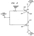
- Electrical circuit 210 is illustrated, which constitutes a circuit analogue of semiconductor device 10 (Fig. 1), at least insofar as circuit 210 is of the normally-off type and achieves low on-resistance.
- Electrical circuit 210 includes a JFET 212 of the high voltage, N-channel type; a bipolar transistor 214 of the low voltage N-P-N type; and an impedance means 216, preferably a resistor, JFET 212 includes a source electrode 216, a drain electrode 218, and a gate electrode 220.
- Bipolar transistor 214 includes a collector electrode 222, an emitter electrode 224, and a base electrode 226.
- Source electrode 216 is ohmically interconnected with collector electrode 222.
- Impedance means 216 is electrically interposed between base electrode 226 and gate electrode 220.
- Electrical circuit 210 advantageously constitutes a three-electrode circuit, with drain electrode 218 serving as a first main current electrode, emitter electrode 224 serving as a second main current electrode, and gate electrode 220 serving as a gate electrode for the entire circuit 210.
- electrical circuit 210 may be provided in discrete form, or they may be individually formed in an integrated circuit, such as semiconductor device 10 of Fig. 1.
- circuit 210 Shorting of gate electrode 220 to first electrode 218 by an appropriate means enables circuit 210 to block forward current (i.e., positive current from first electrode 218 to second electrode 224). Biasing of gate 220 with a positive voltage in excess of about 0.7 volts, at least for silicon devices 212 and 214, permits circuit 210 to conduct forward current with an extremely low on-resistance, inasmuch as the on-resistance of JFET 212 becomes reduced because its P-type gate region (not shown) inject holes into its N-type channel region (not shown).
Landscapes
- Junction Field-Effect Transistors (AREA)
- Bipolar Transistors (AREA)
- Bipolar Integrated Circuits (AREA)
Applications Claiming Priority (2)
| Application Number | Priority Date | Filing Date | Title |
|---|---|---|---|
| US06/455,174 US4506282A (en) | 1983-01-03 | 1983-01-03 | Normally-off semiconductor device with low on resistance and circuit analogue |
| US455174 | 1983-01-03 |
Publications (2)
| Publication Number | Publication Date |
|---|---|
| EP0113334A2 true EP0113334A2 (de) | 1984-07-11 |
| EP0113334A3 EP0113334A3 (de) | 1986-06-11 |
Family
ID=23807690
Family Applications (1)
| Application Number | Title | Priority Date | Filing Date |
|---|---|---|---|
| EP84100025A Withdrawn EP0113334A3 (de) | 1983-01-03 | 1984-01-03 | Im Normalstand abgeschaltete Halbleiteranordnung mit niedrigem Betriebswiderstand und analoge Schaltung |
Country Status (3)
| Country | Link |
|---|---|
| US (1) | US4506282A (de) |
| EP (1) | EP0113334A3 (de) |
| JP (1) | JPS59135760A (de) |
Cited By (2)
| Publication number | Priority date | Publication date | Assignee | Title |
|---|---|---|---|---|
| EP0598794A4 (en) * | 1991-07-30 | 1994-08-10 | Microwave Technology Inc | High frequency jfet and method for fabricating the same. |
| US5567961A (en) * | 1992-08-21 | 1996-10-22 | Hitachi, Ltd. | Semiconductor device |
Families Citing this family (14)
| Publication number | Priority date | Publication date | Assignee | Title |
|---|---|---|---|---|
| GB2174540B (en) * | 1985-05-02 | 1989-02-15 | Texas Instruments Ltd | Intergrated circuits |
| US4714876A (en) * | 1986-04-14 | 1987-12-22 | Ncr Corporation | Circuit for initiating test modes |
| US4799095A (en) * | 1987-07-06 | 1989-01-17 | General Electric Company | Metal oxide semiconductor gated turn off thyristor |
| US6355513B1 (en) * | 1999-10-29 | 2002-03-12 | Lovoltech, Inc. | Asymmetric depletion region for normally off JFET |
| US6492687B2 (en) * | 2001-05-07 | 2002-12-10 | Semiconductor Components Industries Llc | Merged semiconductor device and method |
| US6900506B1 (en) | 2002-04-04 | 2005-05-31 | Lovoltech, Inc. | Method and structure for a high voltage junction field effect transistor |
| US7262461B1 (en) | 2002-05-20 | 2007-08-28 | Qspeed Semiconductor Inc. | JFET and MESFET structures for low voltage, high current and high frequency applications |
| US6921932B1 (en) | 2002-05-20 | 2005-07-26 | Lovoltech, Inc. | JFET and MESFET structures for low voltage, high current and high frequency applications |
| US7268378B1 (en) | 2002-05-29 | 2007-09-11 | Qspeed Semiconductor Inc. | Structure for reduced gate capacitance in a JFET |
| US6777722B1 (en) | 2002-07-02 | 2004-08-17 | Lovoltech, Inc. | Method and structure for double dose gate in a JFET |
| US6696706B1 (en) | 2002-10-22 | 2004-02-24 | Lovoltech, Inc. | Structure and method for a junction field effect transistor with reduced gate capacitance |
| US7075132B1 (en) | 2002-12-30 | 2006-07-11 | Lovoltech, Inc. | Programmable junction field effect transistor and method for programming the same |
| US7038260B1 (en) | 2003-03-04 | 2006-05-02 | Lovoltech, Incorporated | Dual gate structure for a FET and method for fabricating same |
| US9331097B2 (en) * | 2014-03-03 | 2016-05-03 | International Business Machines Corporation | High speed bipolar junction transistor for high voltage applications |
Family Cites Families (2)
| Publication number | Priority date | Publication date | Assignee | Title |
|---|---|---|---|---|
| US4314267A (en) * | 1978-06-13 | 1982-02-02 | Ibm Corporation | Dense high performance JFET compatible with NPN transistor formation and merged BIFET |
| JPS568874A (en) * | 1979-07-04 | 1981-01-29 | Pioneer Electronic Corp | Bipolar transistor device |
-
1983
- 1983-01-03 US US06/455,174 patent/US4506282A/en not_active Expired - Lifetime
- 1983-12-27 JP JP58244958A patent/JPS59135760A/ja active Pending
-
1984
- 1984-01-03 EP EP84100025A patent/EP0113334A3/de not_active Withdrawn
Cited By (2)
| Publication number | Priority date | Publication date | Assignee | Title |
|---|---|---|---|---|
| EP0598794A4 (en) * | 1991-07-30 | 1994-08-10 | Microwave Technology Inc | High frequency jfet and method for fabricating the same. |
| US5567961A (en) * | 1992-08-21 | 1996-10-22 | Hitachi, Ltd. | Semiconductor device |
Also Published As
| Publication number | Publication date |
|---|---|
| US4506282A (en) | 1985-03-19 |
| JPS59135760A (ja) | 1984-08-04 |
| EP0113334A3 (de) | 1986-06-11 |
Similar Documents
| Publication | Publication Date | Title |
|---|---|---|
| US4523111A (en) | Normally-off, gate-controlled electrical circuit with low on-resistance | |
| US4967243A (en) | Power transistor structure with high speed integral antiparallel Schottky diode | |
| US4645957A (en) | Normally-off semiconductor device with low on resistance and circuit analogue | |
| US4969028A (en) | Gate enhanced rectifier | |
| US5014102A (en) | MOSFET-gated bipolar transistors and thyristors with both turn-on and turn-off capability having single-polarity gate input signal | |
| US5396087A (en) | Insulated gate bipolar transistor with reduced susceptibility to parasitic latch-up | |
| US6288424B1 (en) | Semiconductor device having LDMOS transistors and a screening layer | |
| US4961100A (en) | Bidirectional field effect semiconductor device and circuit | |
| US5413313A (en) | Integrated power switch structure having a vertical thyristor controlled by a lateral MOS transistor | |
| US4506282A (en) | Normally-off semiconductor device with low on resistance and circuit analogue | |
| US4969027A (en) | Power bipolar transistor device with integral antisaturation diode | |
| EP0697739B1 (de) | Bipolartransistor mit isolierter Steuerelektrode | |
| IE52758B1 (en) | Gate enhanced rectifier | |
| EP0084558A4 (de) | Monolytisch gemischt aufgebauter feldeffekttransistor und bipolartransistor. | |
| US4743952A (en) | Insulated-gate semiconductor device with low on-resistance | |
| US5294816A (en) | Unit cell arrangement for emitter switched thyristor with base resistance control | |
| US5245202A (en) | Conductivity modulation type misfet and a control circuit thereof | |
| US5412228A (en) | Multifunctional semiconductor switching device having gate-controlled regenerative and non-regenerative conduction modes, and method of operating same | |
| US5608238A (en) | Semiconductor device having two insulated gates and capable of thyristor function and method for operating the same | |
| US6023078A (en) | Bidirectional silicon carbide power devices having voltage supporting regions therein for providing improved blocking voltage capability | |
| US4942440A (en) | High voltage semiconductor devices with reduced on-resistance | |
| US5241194A (en) | Base resistance controlled thyristor with integrated single-polarity gate control | |
| US5440164A (en) | MOS/bipolar device | |
| US5306930A (en) | Emitter switched thyristor with buried dielectric layer | |
| US6975157B1 (en) | Starter device for normally off JFETs |
Legal Events
| Date | Code | Title | Description |
|---|---|---|---|
| PUAI | Public reference made under article 153(3) epc to a published international application that has entered the european phase |
Free format text: ORIGINAL CODE: 0009012 |
|
| AK | Designated contracting states |
Designated state(s): DE FR |
|
| PUAL | Search report despatched |
Free format text: ORIGINAL CODE: 0009013 |
|
| AK | Designated contracting states |
Kind code of ref document: A3 Designated state(s): DE FR |
|
| 17P | Request for examination filed |
Effective date: 19861127 |
|
| 17Q | First examination report despatched |
Effective date: 19881019 |
|
| STAA | Information on the status of an ep patent application or granted ep patent |
Free format text: STATUS: THE APPLICATION HAS BEEN WITHDRAWN |
|
| 18W | Application withdrawn |
Withdrawal date: 19890421 |
|
| R18W | Application withdrawn (corrected) |
Effective date: 19890421 |
|
| RIN1 | Information on inventor provided before grant (corrected) |
Inventor name: BALIGA, BANTVAL JAYANT |