EP0113974A2 - Verfahren und Gerät zur effektiven Hochspannungserzeugung mit Hilfe von Resonanzrücklauf - Google Patents
Verfahren und Gerät zur effektiven Hochspannungserzeugung mit Hilfe von Resonanzrücklauf Download PDFInfo
- Publication number
- EP0113974A2 EP0113974A2 EP83307607A EP83307607A EP0113974A2 EP 0113974 A2 EP0113974 A2 EP 0113974A2 EP 83307607 A EP83307607 A EP 83307607A EP 83307607 A EP83307607 A EP 83307607A EP 0113974 A2 EP0113974 A2 EP 0113974A2
- Authority
- EP
- European Patent Office
- Prior art keywords
- voltage
- resonant
- energy
- frequency
- current
- Prior art date
- Legal status (The legal status is an assumption and is not a legal conclusion. Google has not performed a legal analysis and makes no representation as to the accuracy of the status listed.)
- Withdrawn
Links
- 238000000034 method Methods 0.000 title claims description 27
- 238000006243 chemical reaction Methods 0.000 claims abstract description 57
- 238000003860 storage Methods 0.000 claims abstract description 8
- 238000004804 winding Methods 0.000 claims description 10
- 230000005669 field effect Effects 0.000 claims description 2
- 230000004044 response Effects 0.000 claims description 2
- 230000001360 synchronised effect Effects 0.000 claims description 2
- 230000008901 benefit Effects 0.000 abstract description 7
- 239000003990 capacitor Substances 0.000 description 15
- 230000002441 reversible effect Effects 0.000 description 5
- 230000007423 decrease Effects 0.000 description 3
- 238000013461 design Methods 0.000 description 3
- 230000000694 effects Effects 0.000 description 3
- 230000009471 action Effects 0.000 description 2
- 238000013459 approach Methods 0.000 description 2
- 230000033228 biological regulation Effects 0.000 description 2
- 230000008859 change Effects 0.000 description 2
- 238000010586 diagram Methods 0.000 description 2
- 238000003780 insertion Methods 0.000 description 2
- 230000037431 insertion Effects 0.000 description 2
- 230000001105 regulatory effect Effects 0.000 description 2
- 238000006842 Henry reaction Methods 0.000 description 1
- 230000006978 adaptation Effects 0.000 description 1
- 238000004458 analytical method Methods 0.000 description 1
- 230000035559 beat frequency Effects 0.000 description 1
- 238000004364 calculation method Methods 0.000 description 1
- 238000010276 construction Methods 0.000 description 1
- 238000007796 conventional method Methods 0.000 description 1
- 239000013256 coordination polymer Substances 0.000 description 1
- 230000008878 coupling Effects 0.000 description 1
- 238000010168 coupling process Methods 0.000 description 1
- 238000005859 coupling reaction Methods 0.000 description 1
- 238000013016 damping Methods 0.000 description 1
- 230000003247 decreasing effect Effects 0.000 description 1
- 230000017525 heat dissipation Effects 0.000 description 1
- 230000001939 inductive effect Effects 0.000 description 1
- 238000004519 manufacturing process Methods 0.000 description 1
- 238000012986 modification Methods 0.000 description 1
- 230000004048 modification Effects 0.000 description 1
- 230000010355 oscillation Effects 0.000 description 1
- 230000008569 process Effects 0.000 description 1
- 238000005549 size reduction Methods 0.000 description 1
- 238000012546 transfer Methods 0.000 description 1
- 229910000859 α-Fe Inorganic materials 0.000 description 1
Images
Classifications
-
- H—ELECTRICITY
- H04—ELECTRIC COMMUNICATION TECHNIQUE
- H04N—PICTORIAL COMMUNICATION, e.g. TELEVISION
- H04N3/00—Scanning details of television systems; Combination thereof with generation of supply voltages
- H04N3/10—Scanning details of television systems; Combination thereof with generation of supply voltages by means not exclusively optical-mechanical
- H04N3/16—Scanning details of television systems; Combination thereof with generation of supply voltages by means not exclusively optical-mechanical by deflecting electron beam in cathode-ray tube, e.g. scanning corrections
- H04N3/18—Generation of supply voltages, in combination with electron beam deflecting
- H04N3/185—Maintaining DC voltage constant
Definitions
- the present invention relates to efficient high voltage generation for such applications as cathode-ray-tube (CRT) anode power supplies and the like and other high-voltage, low-current, high-impedance power supplies; being more particularly directed to new and improved methods of and apparatus for such purposes with adaptation for variable-period control and synchronization with external frequencies, if desired.
- CRT cathode-ray-tube
- the charging interval is nearly proportional to the load current at fixed output voltage, and inversely proportional to input voltage.
- the conversion period is the sum of these two intervals so that it, and the conversion frequency, become functions of input voltage and output load current.
- standard control chips such as the TL494, manufactured by Texas Instruments Company, for variable-frequency operation at the cost of a single low-power transistor, so that practical utilization of this technique is feasible with such 85 to 90% efficiencies and significant size reductions. Additionally, reduced temperature rise is attained for enhanced reliability.
- a further advantage is the speed of regulation which is about an order of magnitude faster than customary circuits used for such CRT and related high voltage supplies.
- An object of the invention accordingly, is to provide a new and improved method of and apparatus for high-impedance, very high voltage, very low current voltage generation that is capable of using high speed switching-mode techniques despite the significant stray capacitance and susceptibility to production of resonance at frequencies comparable with the power conversion frequencies, and at high efficiencies.
- a further object is to provide such a novel apparatus in which the expenditure of power for driving the capacitance of the high voltage transformer secondary circuit is advantageously minimized, wherein the secondary circuit is allowed to operate in resonance, and the inductance of the secondary is adjusted to control the resonant frequency to be compatible with the desired conversion frequency.
- the secondary inductance provides the reactive current and power to charge the secondary capacitance both positively and negatively with very little real power loss.
- this is accomplished in resonant flyback operation by injecting a controlled energy into the resonant circuit, as reflected into the primary of the high voltage transformer, during each conversion cycle, and then allowing the resonant circuit complete freedom to resonate or "ring" for a time between a half-cycle and a full-cycle.
- the initial energy less the energy delivered to the load at the voltage peak and less the small circuit losses, is returned to the power source.
- Energy is preferably injected by forcing the input voltage across the transformer primary with a transistor or other electronic switch for a controllable time. Most of the energy is stored in the form of current in the inductor at this point. Therefore, the "charging" time in each conversion cycle is variable over a wide range to accommodate changes in input voltage, output voltage, and load current. Since the resonant flyback interval is subject to less variation under the same changes, it is found that the conversion period and frequency must vary to accommodate input and output conditions. In fact, the circuit is necessarily driven with a variable frequency.
- this is preferably effected by insertion of a variable "dead time" into the conversion cycle by absorbing all of the remaining resonant energy into a resistor at the end of each resonant flyback pulse, so that the circuit may wait an arbitrary length of time before beginning the next conversion cycle.
- a variable "dead time" into the conversion cycle by absorbing all of the remaining resonant energy into a resistor at the end of each resonant flyback pulse, so that the circuit may wait an arbitrary length of time before beginning the next conversion cycle.
- One method of synchronization with the resonant flyback technique of the invention is through the use of a conversion period somewhat shorter than the sync period. This conversion period may then be extended to equal the external sync period by the insertion of a variable "dead time" produced by a heavy damper resistance switched across the inductor after resonant flyback. Such a technique may introduce minimal cost in efficiency of about 10% at full load.
- the invention embraces a method of low-current, high voltage generation for high-impedance application to a load with the aid of a resonant circuit, that comprises, successively switching input energy from a source into the resonant circuit during each power conversion cycle within a desired range of conversion frequencies; adjusting the resonant circuit to enable resonant flyback operation with the storage inductance thereof resonating with its stray capacitance such as to permit free ringing of the same in response to said input energy for a time between a half and a full conversion cycle; delivering energy from said circuit to a load at the voltage peak developed within the circuit; and returning to the source at the end of each conversion cycle the remainder of the input energy after such energy delivery to the load, thus generating high efficiency operation over wide input voltage ranges.
- Preferred constructions and best mode embodiments are hereinafter set forth.
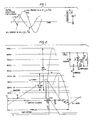
- Fig. 1 is a graph plotting current and voltage waveforms in an ideal lossless resonant LC circuit
- a capacitor C and inductor L are shown in parallel forming a resonant circuit. If electrical energy is injected into this circuit, a sinusoidal oscillation of voltage and current will result which will persist (or “ring") after the energy source is disconnected. The total energy remains constant as it alternates between electrostatic energy in the capacitance C and electromagnetic energy in the inductor C, with sinusoidal current (i) and voltage (e) waveforms 90 degrees apart as illustrated along the horizontal time axis in Fig. 1. At the current peak (ipk), the voltage is zero so that all of the resonant energy is stored in the inductor as current. At the voltage peak (epk), 90 degrees or a quarter-cycle later, the current has become zero and all the resonant energy is stored in the capacitor C as voltage. This situation establishes the basic relationship between the peak values of voltage and current.
- One method of injecting energy into the parallel resonant circuit of Fig. 1 is to connect a low-impedance DC voltage source E across the circuit for a time "t".
- the capacitor voltage quickly rises to the applied voltage and remains there, while the inductor current begins to rise from zero at a linear rate.
- the total energy W stored in the resonant circuit is:
- a 132-volt DC input voltage E is switched across the resonant circuit comprised of a 2.00mH inductor L and 9.39nF capacitor C by a switch S to ground which is closed for a time tl.
- the circuit is shown provided with a load R and a rectifier D connected across the resonant L-C circuit.
- the switch opens, the voltage "e" rises in resonance toward a peak of 919 volts from ground, or 787 volts given by the above equation above its reference of the +132-volt input.
- the inductor current "i” actually continues to increase slightly while voltage "e” is less than the 132- volt level, true to its resonant equations. Above the 132-volt point, the inductor current begins to decline as expected. When the voltage "e” reaches 318 volts above the 132-volt input and the rectifier D begins to conduct, the inductor current has dropped to 1.5 amperes from an initial 1.68 amperes.
- a filter capacitor Cf is connected across the load and is made large enough so that its voltage rises imperceptably in the waveform of Fig. 2 during conduction of the rectifier D.
- the rectifier D is able to divert the inductor current from its previous path through the resonant capacitor C to the filter capacitor Cf and its load R.
- Voltage "e” is then held constant at 318 volts above the 132-volt input while inductor current flows through the rectifier D.
- the voltage across C is constant so that its current is zero. Since the voltage across inductor L is also constant, its current is decreasing linearly with time rather than sinusoidally.
- the rectifier current is the same as the inductor current and has a linear sawtooth waveshape.
- the DC load current is the average of this sawtooth shape over a 56 ⁇ S conversion period, or 137mA.
- the inductor current reaches zero while moving negatively. There is no longer any current available for forward conduction in the rectifier D, and it becomes non-conductive. Since the inductor current is zero, its stored energy is also zero, and the only resonant energy that remains is the 318-volt charge on the capacitor A. A new "initial condition" has now been established on the resonant circuit in which the e 1 pk is now 318 volts above the 132-volt reference. The voltage "e” then falls in free resonance and reaches the 132-volt line in a quarter- period of resonance, then continues toward zero voltage while the inductor current becomes negative in sinusoidal fashion.
- Time interval t5 ends as "e” reaches zero and the switch S is closed once again to begin the following conversion cycle.
- the inductor current has now reached -0.63 amperes, and closure of the switch passes this current back to the 132- volt source.
- a fixed voltage of 132 volts now exists across the inductor L, so its current begins a positive linear change from the initial -0.63 ampere point.
- Energy is returned to the 132-volt source until the inductor current reaches zero at point t0, after which energy is once again withdrawn from this source.
- the current has changed from -0.63 to +1.68A and the switch S opens to repeat the above cycle of energy conversion, with the switch successively and repetitively applying the input voltage during each conversion cycle.
- the inductor energy at I 0 of 1.68A (2.822mJ) less the inductor energy at I 1 of 0.63A (0.397mJ) is the energy delivered to the load R, or 2.43mJ, since the energy in C is the same at toth points.
- This energy equals 318 volts DC output at 137mADC for 56 ⁇ S.
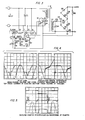
- Fig. 3 represents a simplified schematic of a resonant flyback high voltage power supply embodying the technique of the invention including the type of operation described in connection with Fig. 2.
- a four-rectifier voltage multiplier is shown at D 2 -D 5 which will deliver a HVDC output approaching twice the peak-to-peak voltage delivered by the secondary winding L S of power transformer Tl.
- any number of "full-wave" multiplier stages may be used, to at least seven, for a 50KV output.
- the secondary inductance L S is designed to deliver a peak-to-peak voltape equal to the maximum high voltage DC output divided by the number of full-wave multiplier stages (or by twice the number of rectifiers) at the lowest desired operating frequency.
- Fig. 2 illustrates a half-wave rectifier D in which energy flows to the load R through the rectifier D only during the positive flyback peaks
- the full-wave rectifiers D 2 -D 5 of Fig. 3 pass energy to the load on both the positive and negative peaks.
- the energy transferred on the positive peak is from resonant flyback action, while that transferred on the negative peak is by ordinary transformer action with switch Ql conducting and placing the full input voltage on the transformer primary L P .
- Capacitor Cs represents the unavoidable stray capacitance of capacitors C3 and C4 to ground, plus the internal winding capacitance of the transformer secondary L S itself. It is reflected into the transformer primaryL p as a capacitance N 2 times as large as C S , where N is the turns ratio of transformer T 1 (represented as capacitance "C" in Fig. 2).
- transformer T 1 may normally use a ferrite core which contains an air gap adjusted to obtain a secondary inductance IS which will resonate C S at the desired frequency.
- the value of I S is then reflected into the primary as 1/N 2 times L S (which is equivalent to "L" of Fig. 2).
- the transformer primary L P is designed so that its peak-to-peak voltage at minimum HV output is somewhat more than twice the maximum input voltage, say 2.2 times.
- the transformer turns ratio "N" is then the ratio of the peak-to-peak voltages of the secondary to that of the primary.
- Primary-to-secondary coupling must be "tight" to minimize leakage inductance while maintaining high-voltage integrity in the secondary L S . Energy stored in the leakage inductance cannot be delivered to the output but must be dissipated by damper resistor R4 converted with capacitor C 2 between the lower terminal of I P and the terminal of the input voltage.
- the switch Q 1 is illustrated in the form of field-effect transistor (FET), serving as the power switch.
- FET field-effect transistor
- the integral reverse diode in the FET is also of value in conducting the reverse current I 1 (Fig. 2) after the resonant flyback fall during t5.
- the FET power switch Q 1 may be driven directly by a conventional PWM integrated circuit such as the TL494 shown in Fig. 3, embodying a saw-tooth oscillator OSC, operational amplifier A and output transistor Q 3 for driving the FET switch Q 1 .
- the TL494 generates a positive-slope sawtooth (waveform shown at right of OSC) which is compared with the amplified error signal from the internal operational amplifier A.
- the output stage transistor Q 3 is turned on, and drives Q 1 on, when this sawtooth is more positive than the amplified error voltage terminal 3 of the TL494 Therefore, the desired negative feedback for voltage regulation is achieved by feeding the 5-volt sample of the high voltage output into the + terminal of the operational amplifier A; and the 5-volt reference, into the - terminal of A through R 8 .
- the damping of the regulating loop is controlled by C 7 and R 7 .
- This circuit is reasonably tolerant of timing errors.
- the reverse current I 1 in Fig. 2 will flow through the integral reverse diode of Q 1 and prevent the drain voltage "e" from passing negatively through ground.
- the gate of Q 1 may be turned on at any time between the end of interval t 5 and t 0 without changing the operating condition of the circuit.
- the output control of this resonant flyback circuit is primarily through modulation of the conversion frequency by Q 2 .
- the waveforms of Fig. 4 illustrate the performance of a resonant-flyback converter operating from a 160-volt DC input and delivering 24KV from a four-stage (full-wave) voltage multiplier of the type shown in Fig. 3.
- the "ringing" present in the current waveforms is at the frequency of resonance between the transformer leakage inductance and the secondary stray capacitance as reflected into the primary Lp.
- the current waveform is also seen to rise positively immediately after the drain voltage falls to zero, rather than flowing negatively as at 24 ⁇ A load. This positive rise represents current required for charging the voltage multiplier on its negative voltage peak using simple transformer conversion.
- a small positive spike will also be observed on the drain voltage waveform at the instant the drain current is cut off. This is the usual leakage inductance spike which is controlled with the damper C 2 and R 4 of Fig. 3.
- the usual starting point in a resonant flyback design of the invention is to define the parameters of input voltage range, output voltage range, output load range, maximum conversion period (minimum frequency), and secondary stray capacitance load, Cs.
- Cs is reflected to the primary as a capacitance N 2 larger .
- the primary inductance L may be calculated from the energy and timing relationships. This calculation should be made for the lowest input voltage, and maximum conversion period, output voltage, and load.
- KnowingL one may determine the timing requirements for tie driver under all input and output conditions, and the peak current rating for the switch transistor Q l .
- Sensing of the output load current by means of a resistor inserted in the ground return of the high voltage multiplier affords a signal which may be used in TL494 for the purpose of current-limiting and overload protection.
- a "current sense latch”, such as of the type SG1549, for example is very effective protection when used to monitor the source or drain current in Q 1 and drive terminal 4 of TL494 off when excessive currents are experienced.
- the drain current of Q 1 increases rapidly when it is turned on, limited only by the leakage inductance of T l .
- the SG1549 is able to respond quickly, and the FET used for Q 1 also shuts down very quickly because of its lack of storage time, so that continuous operation into a short circuit with very small input power consumption is possible.
- Such a system synchronized to a TV linescan frequency of 15.75KHz, for example, operates with the waveforms of Fig. 5. It is operating from a 134-volt input and generating a 24KV output of 24 ⁇ A.
- the bottom trace is the drain-source waveform of Q 1 at 100 volts per division and shows two flyback pulses with a "dead time" between them produced by a switched damper.
- the top trace is the damper control waveform, in which the negative portion switches the damper on.
- the center trace is the drain current in Q 1 at 1 ampere per division. Its ringing is at the frequency of resonance between the transformer leakage inductance and the secondary stray capacitance Cs as reflected into the primary.
- phase comparator uses a phase comparator to compare the conversion frequency with an external frequency.
- the output signal of the phase comparator is then used to control the conversion frequency by modulation of either or both of the resonant components, L or C, to form a phase-locked-loop system.
- the switching mode-resonant flyback technique of the invention thus provides a method of obtaining the considerable advantages of very high power efficiency over a wide input voltage range in the design of high voltage power supplied.
- this resonant flyback scheme may carefully be employed to convert power from low voltages, say 20 to 180VDC, to very high voltage, say 10KV to 50KV, at power levels from about 10 to 200 watts and with high impedance in the range of 1-250 Megohms. Power conversion efficiencies of 85 to 90% have been achieved which are almost constant over an unusually wide input voltage range. The advantages of small size and very low heat dissipation which have made switching-mode techniques so successful in low voltage power supplies are thus now accessible to designers of high voltage supplies.
- variable frequency (or Period) output control circuits with a resonant high-voltage transformer to enable efficient generation of high voltage power when the transformer resonant frequency is comparible with the desired range of conversion frequencies.
- the output power is in the form of an assymetric alternating voltage which may be used directly or may be applied to conventional voltage-multiplying rectifiers for generation of high D. C. voltages.
- Control may be open or closed loop for regulated performance. Through the use of a switched damper, residual resonant energy may be absorbed after each conversion cycle and synchronization may be attained with external frequencies.
- the variable-period control-resonant transformer system is particularly adapted to achieve frequency synchronization with the reactance switch control by phase locked loop.
Landscapes
- Engineering & Computer Science (AREA)
- Multimedia (AREA)
- Signal Processing (AREA)
- Dc-Dc Converters (AREA)
- Rectifiers (AREA)
- Details Of Television Scanning (AREA)
Applications Claiming Priority (2)
| Application Number | Priority Date | Filing Date | Title |
|---|---|---|---|
| US06/450,532 US4616300A (en) | 1982-12-17 | 1982-12-17 | Method of and apparatus for efficient high voltage generation by resonant fly back |
| US450532 | 1982-12-17 |
Publications (2)
| Publication Number | Publication Date |
|---|---|
| EP0113974A2 true EP0113974A2 (de) | 1984-07-25 |
| EP0113974A3 EP0113974A3 (de) | 1986-02-05 |
Family
ID=23788460
Family Applications (1)
| Application Number | Title | Priority Date | Filing Date |
|---|---|---|---|
| EP83307607A Withdrawn EP0113974A3 (de) | 1982-12-17 | 1983-12-14 | Verfahren und Gerät zur effektiven Hochspannungserzeugung mit Hilfe von Resonanzrücklauf |
Country Status (4)
| Country | Link |
|---|---|
| US (1) | US4616300A (de) |
| EP (1) | EP0113974A3 (de) |
| JP (1) | JPS59171365A (de) |
| CA (1) | CA1208284A (de) |
Cited By (3)
| Publication number | Priority date | Publication date | Assignee | Title |
|---|---|---|---|---|
| GB2209856A (en) * | 1985-05-10 | 1989-05-24 | Rca Licensing Corp | Regulating power supply for video display apparatus |
| EP0350191A3 (de) * | 1988-07-08 | 1990-10-31 | FERRANTI INTERNATIONAL plc | Push-pull-Resonanzschaltmodenleistungsversorgungssperrwandler |
| EP0356661A3 (de) * | 1988-08-26 | 1991-07-17 | GRUNDIG E.M.V. Elektro-Mechanische Versuchsanstalt Max Grundig holländ. Stiftung & Co. KG. | Geregeltes Schaltnetzteil mit Hochspannungsgenerator für ein Fernsehgerät |
Families Citing this family (37)
| Publication number | Priority date | Publication date | Assignee | Title |
|---|---|---|---|---|
| US4709316A (en) * | 1985-12-27 | 1987-11-24 | General Electric Company | Single-ended DC-to-DC converter with lossless switching |
| KR900008542B1 (ko) * | 1986-10-13 | 1990-11-24 | 가부시기가이샤 히다찌세이사구쇼 | 마이크로파 가열장치의 전원 |
| US4812960A (en) * | 1986-12-15 | 1989-03-14 | Matsushita Electric Industrial Co., Ltd. | Power feeding apparatus |
| US4757433A (en) * | 1987-01-07 | 1988-07-12 | Display Components, Inc. | Power supply |
| US4823248A (en) * | 1987-04-07 | 1989-04-18 | Murata Manufacturing Co., Ltd. | High voltage generator |
| US4945464A (en) * | 1987-06-15 | 1990-07-31 | Varian Associates, Inc. | High voltage DC power supply |
| EP0303994B1 (de) * | 1987-08-21 | 1993-05-05 | Nippon Telegraph And Telephone Corporation | Push-Pull-Stromgespeister Gleichstromwandler |
| US4888821A (en) * | 1988-12-09 | 1989-12-19 | Honeywell Inc. | Synchronization circuit for a resonant flyback high voltage supply |
| CA1316980C (en) * | 1988-12-27 | 1993-04-27 | Daniel C. Hughey | Power supply |
| US4964028A (en) * | 1989-10-26 | 1990-10-16 | Plessey Electronic Systems Corp. | Current limited quasi-resonant voltage converting power supply |
| US5003451A (en) * | 1989-12-21 | 1991-03-26 | At&T Bell Laboratories | Switched damper circuit for dc to dc power converters |
| DE4006441A1 (de) * | 1990-03-01 | 1991-09-05 | Eltex Elektrostatik Gmbh | Variabler hochspannungsgenerator |
| US5458217A (en) * | 1991-05-01 | 1995-10-17 | Bridgestone Corporation | Electrorheological fluid damping control system having high voltage power supply |
| IT1247356B (it) * | 1991-06-17 | 1994-12-12 | Plessey Spa | Apparecchiatura per la generazione di alta tensione continua stabilizzata in particolare per l'impiego in combinazione con una marmitta anti-inquinamento |
| US5455757A (en) * | 1994-01-28 | 1995-10-03 | Compaq Computer Corp. | Power converter having regeneration circuit for reducing oscillations |
| US5377091A (en) * | 1994-01-28 | 1994-12-27 | Compaq Computer Corporation | Power converter having regeneration circuit for reducing oscillations |
| SE512406C2 (sv) * | 1994-05-02 | 2000-03-13 | Ericsson Telefon Ab L M | Anordning och förfarande vid spänningsomvandlare |
| FR2724786B1 (fr) * | 1994-09-16 | 1996-12-20 | Sames Sa | Procede et dispositif d'elaboration de haute tension, notamment pour l'application electrostatique de produit de revetement |
| US5691889A (en) * | 1995-12-13 | 1997-11-25 | Unitrode Corporation | Controller having feed-forward and synchronization features |
| US5754414A (en) * | 1996-02-23 | 1998-05-19 | Hanington; Gary J. | Self-compensating switching power converter |
| US5680036A (en) * | 1996-03-19 | 1997-10-21 | Compaq Computer Corporation | Logarithmic power compensation for a switching power supply |
| US6067236A (en) * | 1997-11-03 | 2000-05-23 | Rantec Microwave & Electronics Inc. | Power supply for providing high voltage power from a low voltage source |
| JP2001218466A (ja) * | 2000-02-03 | 2001-08-10 | Sony Corp | 高電圧安定化回路 |
| US6483731B1 (en) * | 2000-07-31 | 2002-11-19 | Vanner, Inc. | Alexander topology resonance energy conversion and inversion circuit utilizing a series capacitance multi-voltage resonance section |
| AR030511A1 (es) * | 2000-12-22 | 2003-08-20 | Patricio Lagos Lehuede | Un inversor o convertidor por inyeccion de corriente provisto de un circuito cuya frecuencia de generacion de la tension alterna esta ajustada por la frecuencia de resonancia de la carga, ciclo a ciclo, sin retardos |
| KR100491599B1 (ko) * | 2002-08-29 | 2005-05-27 | 삼성전자주식회사 | 고압전원장치 |
| JP4774903B2 (ja) * | 2005-10-17 | 2011-09-21 | サンケン電気株式会社 | スイッチング電源装置 |
| EP2025051B1 (de) | 2006-06-06 | 2014-12-31 | Ideal Power Inc. | Universeller stromrichter |
| US8514601B2 (en) | 2009-08-17 | 2013-08-20 | Ideal Power Converters, Inc. | Power conversion with added pseudo-phase |
| CN102714465A (zh) | 2009-06-29 | 2012-10-03 | 理想能量转换器有限公司 | 带有旁路能量转移电抗的消弧开关的功率转移器件、方法和系统 |
| CA2808490C (en) | 2009-08-17 | 2015-02-03 | Ce+T Energy Solutions Inc. | Power conversion with added pseudo-phase |
| PH12013501097A1 (en) | 2010-11-30 | 2016-08-05 | Ideal Power Inc | Photovoltaic array systems, methods, and devices with bidirectional converter |
| US8531858B2 (en) | 2011-02-18 | 2013-09-10 | Ideal Power, Inc. | Power conversion with current sensing coupled through saturating element |
| US9808547B2 (en) | 2013-04-18 | 2017-11-07 | Dm Tec, Llc | Sanitizer |
| US9950086B2 (en) | 2014-03-12 | 2018-04-24 | Dm Tec, Llc | Fixture sanitizer |
| US9700643B2 (en) | 2014-05-16 | 2017-07-11 | Michael E. Robert | Sanitizer with an ion generator |
| US10124083B2 (en) | 2015-06-18 | 2018-11-13 | Dm Tec, Llc | Sanitizer with an ion generator and ion electrode assembly |
Family Cites Families (6)
| Publication number | Priority date | Publication date | Assignee | Title |
|---|---|---|---|---|
| FR1567257A (de) * | 1968-03-08 | 1968-05-16 | ||
| US4106086A (en) * | 1976-12-29 | 1978-08-08 | Rca Corporation | Voltage multiplier circuit |
| JPS5571355A (en) * | 1978-11-24 | 1980-05-29 | Toshiba Corp | High voltage generation circuit |
| DE3068361D1 (en) * | 1979-10-04 | 1984-08-02 | Ici Plc | A d.c. to d.c. converter |
| US4318165A (en) * | 1980-04-21 | 1982-03-02 | General Electric Company | Resonant-flyback power supply with filament winding for magnetron and the like loads |
| JPS5713965A (en) * | 1980-06-27 | 1982-01-25 | Morita Mfg Co Ltd | Direct current high voltage generating device |
-
1982
- 1982-12-17 US US06/450,532 patent/US4616300A/en not_active Expired - Fee Related
-
1983
- 1983-12-14 EP EP83307607A patent/EP0113974A3/de not_active Withdrawn
- 1983-12-16 CA CA000443545A patent/CA1208284A/en not_active Expired
- 1983-12-17 JP JP58238723A patent/JPS59171365A/ja active Pending
Cited By (4)
| Publication number | Priority date | Publication date | Assignee | Title |
|---|---|---|---|---|
| GB2209856A (en) * | 1985-05-10 | 1989-05-24 | Rca Licensing Corp | Regulating power supply for video display apparatus |
| GB2209856B (en) * | 1985-05-10 | 1990-01-04 | Rca Licensing Corp | Regulating power supply for video display apparatus |
| EP0350191A3 (de) * | 1988-07-08 | 1990-10-31 | FERRANTI INTERNATIONAL plc | Push-pull-Resonanzschaltmodenleistungsversorgungssperrwandler |
| EP0356661A3 (de) * | 1988-08-26 | 1991-07-17 | GRUNDIG E.M.V. Elektro-Mechanische Versuchsanstalt Max Grundig holländ. Stiftung & Co. KG. | Geregeltes Schaltnetzteil mit Hochspannungsgenerator für ein Fernsehgerät |
Also Published As
| Publication number | Publication date |
|---|---|
| CA1208284A (en) | 1986-07-22 |
| EP0113974A3 (de) | 1986-02-05 |
| US4616300A (en) | 1986-10-07 |
| JPS59171365A (ja) | 1984-09-27 |
Similar Documents
| Publication | Publication Date | Title |
|---|---|---|
| US4616300A (en) | Method of and apparatus for efficient high voltage generation by resonant fly back | |
| CN107979287B (zh) | 用于主开关切换转换的零电压开关式逆变器 | |
| EP0508664B1 (de) | Gleichspannungswandler | |
| EP0837546B1 (de) | Leistungsschaltung | |
| KR100354728B1 (ko) | 방전절연차단을위해전압펄스시퀀스를발생시키는회로장치 | |
| US6519168B2 (en) | High frequency DC to AC inverter | |
| US4845605A (en) | High-frequency DC-DC power converter with zero-voltage switching of single primary-side power device | |
| US5777859A (en) | Voltage converter | |
| US5909362A (en) | Resonant power converter | |
| CN1312833C (zh) | 直流电压变换电路 | |
| US6961256B2 (en) | Synchronous rectifier with dead time adjusting function | |
| JP2001197740A (ja) | スイッチング電源装置 | |
| US7414864B2 (en) | Switching power supply apparatus | |
| KR20010078125A (ko) | 고전압 안정화회로 | |
| US11043890B2 (en) | Controller with frequency to on-time converter | |
| Ivensky et al. | A resonant dc-dc transformer | |
| US4951186A (en) | Single-ended forward frequency converter with a transformer and a demagnetization means | |
| US4839915A (en) | Inverter type X-ray apparatus | |
| EP1032968B1 (de) | Schaltnetzteil | |
| US4227125A (en) | Regulated deflection system | |
| US4301394A (en) | Horizontal deflection circuit and power supply with regulation by horizontal output transistor turn-off delay control | |
| CN117175947A (zh) | 具有开关控制电路系统的电压转换器 | |
| US11146175B2 (en) | One-sided parallel LLC power converter | |
| KR100916488B1 (ko) | 입력 전원 스위칭과 동기화된 전원장치 | |
| Cheng et al. | Zero switching low output voltage power factor correction circuits |
Legal Events
| Date | Code | Title | Description |
|---|---|---|---|
| PUAI | Public reference made under article 153(3) epc to a published international application that has entered the european phase |
Free format text: ORIGINAL CODE: 0009012 |
|
| AK | Designated contracting states |
Designated state(s): AT BE CH DE FR GB IT LI LU NL SE |
|
| RBV | Designated contracting states (corrected) |
Designated state(s): DE FR GB IT SE |
|
| PUAL | Search report despatched |
Free format text: ORIGINAL CODE: 0009013 |
|
| AK | Designated contracting states |
Designated state(s): DE FR GB IT SE |
|
| STAA | Information on the status of an ep patent application or granted ep patent |
Free format text: STATUS: THE APPLICATION IS DEEMED TO BE WITHDRAWN |
|
| 18D | Application deemed to be withdrawn |
Effective date: 19861006 |
|
| RIN1 | Information on inventor provided before grant (corrected) |
Inventor name: SANTELMANN, WILLIAM FREDERICK, JR. |