EP0114228A2 - Procédé de réalisation d'un condensateur sur un substrat - Google Patents
Procédé de réalisation d'un condensateur sur un substrat Download PDFInfo
- Publication number
- EP0114228A2 EP0114228A2 EP83111406A EP83111406A EP0114228A2 EP 0114228 A2 EP0114228 A2 EP 0114228A2 EP 83111406 A EP83111406 A EP 83111406A EP 83111406 A EP83111406 A EP 83111406A EP 0114228 A2 EP0114228 A2 EP 0114228A2
- Authority
- EP
- European Patent Office
- Prior art keywords
- layer
- depositing
- thin film
- amorphous thin
- ferroelectric
- Prior art date
- Legal status (The legal status is an assumption and is not a legal conclusion. Google has not performed a legal analysis and makes no representation as to the accuracy of the status listed.)
- Granted
Links
Images
Classifications
-
- H—ELECTRICITY
- H01—ELECTRIC ELEMENTS
- H01G—CAPACITORS; CAPACITORS, RECTIFIERS, DETECTORS, SWITCHING DEVICES, LIGHT-SENSITIVE OR TEMPERATURE-SENSITIVE DEVICES OF THE ELECTROLYTIC TYPE
- H01G4/00—Fixed capacitors; Processes of their manufacture
- H01G4/002—Details
- H01G4/018—Dielectrics
- H01G4/20—Dielectrics using combinations of dielectrics from more than one of groups H01G4/02 - H01G4/06
-
- H—ELECTRICITY
- H10—SEMICONDUCTOR DEVICES; ELECTRIC SOLID-STATE DEVICES NOT OTHERWISE PROVIDED FOR
- H10B—ELECTRONIC MEMORY DEVICES
- H10B53/00—Ferroelectric RAM [FeRAM] devices comprising ferroelectric memory capacitors
-
- H—ELECTRICITY
- H10—SEMICONDUCTOR DEVICES; ELECTRIC SOLID-STATE DEVICES NOT OTHERWISE PROVIDED FOR
- H10D—INORGANIC ELECTRIC SEMICONDUCTOR DEVICES
- H10D1/00—Resistors, capacitors or inductors
- H10D1/60—Capacitors
- H10D1/68—Capacitors having no potential barriers
-
- Y—GENERAL TAGGING OF NEW TECHNOLOGICAL DEVELOPMENTS; GENERAL TAGGING OF CROSS-SECTIONAL TECHNOLOGIES SPANNING OVER SEVERAL SECTIONS OF THE IPC; TECHNICAL SUBJECTS COVERED BY FORMER USPC CROSS-REFERENCE ART COLLECTIONS [XRACs] AND DIGESTS
- Y10—TECHNICAL SUBJECTS COVERED BY FORMER USPC
- Y10T—TECHNICAL SUBJECTS COVERED BY FORMER US CLASSIFICATION
- Y10T29/00—Metal working
- Y10T29/43—Electric condenser making
- Y10T29/435—Solid dielectric type
Definitions
- This invention relates to a method of forming a capacitor on a substrate, and more particularly, to a method of forming a capacitor with dual dielectrics wherein one of the dielectric layers is formed by laser annealing.
- Titanates and zirconates are complex inorganic compounds which in crystalline form exhibit a high dielectric constant and ferroelectric properties. As a result of their high dielectric constants, the ferroelectric forming titanates and zirconates have been employed as capacitor dielectrics.
- Some common titanates used in capacitor applications include CaTi0 3 , SrTiO 3 , BaTi0 3 and PbTi0 3 .
- Some common zirconates used in capacitor applications include lead zirconate titanate (PZT) and lead zirconate lanthanum modified titanate (PZLT).
- titanates or zirconates In order to obtain the highest capacitance per unit area, it is necessary to prepare a thin crystalline film of the titanate or zirconate.
- ferroelectric forming titanates or zirconates are deposited in thin film form, they are generally amorphous, and exhibit low dielectric constants.
- the thin film In order to form crystalline thin films of titanates or zirconates, the thin film must be deposited at high temperatures, e.g., by sputtering, or deposited at low temperatures and subsequently annealed at high temperatures.
- high temperature deposition or high temperature post deposition annealing produce other undesirable effects.
- these high temperature processes produce Pb vacancies, oxygen diffusion or other stoichiometric changes in the thin film structure which effect the dielectric constant thereof. These changes vary from run to run so that large and unpredictable variations in dielectric constant result.
- high temperature processing has deleterious effects on the other active devices (e.g., transistors) on an integrated circuit chip so that overall chip performance is degraded.
- the invention as claimed is intended to remedy the mentioned drawbacks. It solves the problem of providing a method of forming a capacitor on a substrate, which capacitor has high dielectric constant and low leakage current. Furthermore the disclosed method does not produce other undesirable effects and provides capacitors having controllable and repeatable properties.
- the dual dielectric comprises a first dielectric layer adjacent one of the electrodes, for preventing the flow'of leakage currents across the electrodes.
- the second dielectric layer is a high dielectric constant layer which is formed by laser annealing an amorphous thin film layer of a ferroelectric forming titanate or zirconate to a ferroelectric.
- the capacitor structure of the present invention exhibits a low leakage value as a result of the leakage current blocking first dielectric layer, and a high dielectric constant as a result of the ferroelectric titanate or zirconate second dielectric layer.
- the second dielectric layer is formed by laser annealing a thin film of a ferroelectric forming titanate or zirconate to a ferroelectric, none of the undesirable effects of high temperature deposition or high temperature post annealing are present. More particularly, since laser pulse intensity and duration are easily controlled, uniform capacitor properties may be obtained from chip to chip. Laser annealing also produces instantaneous heating so that Pb vacancies, oxygen diffusion or other stoichiometric changes do not take place.
- a capacitor according to the present invention may be fabricated by a process of depositing a bottom electrode on an substrate, depositing an amorphous thin film layer of a ferroelectric forming titanate or zirconate on the bottom electrode and depositing a leakage current blocking dielectric layer on the amorphous thin film layer.
- the ferroelectric forming titanate or zirconate is then laser annealed to the ferroelectric phase and a top electrode is deposited on the dielectric layer.
- the leakage current blocking dielectric layer may also serve as an antireflective coating for the titanate or zirconate layer so that better coupling of the laser energy to the titanate or zirconate layer is obtained.
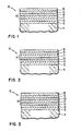
- Capacitor 10 is fabricated on silicon semiconductor or ceramic substrate 11, as a part of an integrated circuit chip or multilayer ceramic structure.
- Substrate 11 optionally may include a thin (approximately 50-500 nm) layer 12 of Si0 2 for isolating the capacitor therefrom.
- Capacitor 10 comprises bottom electrode 13, dielectric 14 and top electrode 15.
- Bottom electrode 13 is preferably a dual bottom electrode structure as will be described more particularly below.
- Dielectric 14 comprises a dual dielectric structure as described more particularly below.
- Top electrode 15 is here shown as a single layer although a multilayer structure may also be employed.
- a passivating layer 16'of SiO 2 may be formed on top electrode 15.
- capacitor 10 may be formed directly on substrate 11 or upon an Si0 2 passivating layer 12 grown thereon.
- Bottom electrode 13 is then formed. While bottom electrode 13 may be a single layer, e.g., PtSi, TiN or Ti 10 W 90 alloy directly on substrate 11, or TiN, TiW, Ti or Ta on SiO 2 passivating layer 12, it is preferably a dual bottom electrode structure as described in European patent application 81 105 741.3.
- bottom electrode 13 is formed by electron beam evaporating or sputtering a first layer of Zr, Hf or Ta (thickness 50-70 nm) on SiO 2 passivating layer 12 and then sputtering a Pt layer (thickness 1000 nm) thereon.
- the dual bottom electrode structure is then heat treated to form an intermetallic phase of Z r P t 3 , H f P t 3 , or TaPt3as described in the above referenced European patent application.
- Dielectric 14 is then formed on bottom electrode 13. Referring to Fig. 1, dielectric layer 14 comprises a high dielectric constant layer 17 and a leakage current preventing dielectric layer 18.
- High dielectric constant layer 17 comprises a thin film (approximately 20-80 nm) of a ferroelectric forming titanate or zirconate, e.g., PbTiO 3 , BaTiO 3 , CaTiO 3 , SrTiO 3 , PZT or PZLT.
- Amorphous thin films of BaTi03 may be formed by sputtering in an Rf diode (2kw) system using a target approximately 20 cm in diameter having a pressed target material of approximately 80% of the theoretical density. When sputtered in argon (AR) plasma at 750 or 1000 watts and 13 ⁇ bar total pressure, a deposition rate of 9.3-11 nm per minute is obtained.
- a refractive index of 1.91-1.93 and dielectric constant of approximately 18 is obtained.
- BaTi0 3 films of comparable thickness may be prepared in an Ar-10% 0 2 plasma.
- PZT or PZLT films may be prepared from an 20 cm target (80% theoretical density) using similar deposition conditions. For the same power levels, deposition rates of approximately 20 nm per minute are obtained.
- a refractive index of 1.9-2.2 and a dielectric constant of approximately 45 is obtained.
- Amorphous thin films of other ferroelectric forming zirconates and titanates may be prepared in a like manner.
- the amorphous thin film ferroelectric forming titanate or zironcate layer 17 is then laser annealed to the high dielectric constant ferroelectric phase.
- a cw-Ar, Q switched ruby, Nd-yag, C0 2 or other laser may be employed.
- a 420 nm dye laser in pulses of 10 nanoseconds having a peak power of approximately 65 watts may be employed to anneal a thin BaTiO 3 film. Under these conditions, laser annealing increases the BaTiO 3 dielectric constant from approximately 18 to over 500 for a thirty fold increase. Laser annealing other titanates or zirconates will increase the dielectric constant ten to fifty times.
- the laser may be used to anneal the entire layer 17.
- a thin laser beam may scan layer 17 to form alternate portions of laser annealed and unannealed titanate or zirconate.
- Layer 18 may comprise Si 3 N 4 , A1203, or SiO 2 (a pp roxi- mately 20-200 nm) and may be deposited by processes well known to those having skill in the art. It will be noted, however, that such deposition processes must be low temperature (less than about 350°C) deposition processes, e.g., low temperature chemical vapor deposition (CVD), plasma enhanced deposition, or rf sputtering on water cooled substrates so that the deleterious effects of high temperature processing on laser annealed dielectric layer 18 do not occur.
- CVD low temperature chemical vapor deposition
- plasma enhanced deposition or rf sputtering on water cooled substrates so that the deleterious effects of high temperature processing on laser annealed dielectric layer 18 do not occur.
- top electrode 15 which may be Al, alloys thereof, or multiple metal layers, is deposited thereon.
- An Si0 2 passivating layer 16 may be formed on top electrode 16.
- contacts to top electrode 16 may be made using standard photolithographic processes.
- leakage blocking dielectric layer 19 is first deposited, followed by laser annealed high dielectric constant layer 17.
- the composition and process of forming high dielectric constant layer 17 is the same as Fig. 2.
- the composition of leakage blocking dielectric layer 19 is the same as that of leakage blocking layer 18 of Fig. 2.
- leakage blocking layer 19 may be formed by high temperature (i.e., approximately 800°C) CVD, sputtering or other high temperature deposition techniques. This contrasts with Fig. 1 wherein leakage blocking layer 18 had to be formed by low temperature (i.e., less than about 350°C) techniques, to prevent undesirable stoichiometric effects in laser annealed layer 17.
- a dual dielectric A preferred method of forming a dual dielectric according to the present invention will now be described.
- an amorphous thin film layer 17 of ferroelectric forming zirconate or titanate is formed.
- Leakage current preventing dielectric layer 18 is then deposited on layer 17.
- Layer 17 is then laser annealed by passing a laser beam through layer 18 into layer 17.
- leakage current preventing dielectric layer 18 also functions as an antireflective coating (ARC) to minimize reflection and increase laser absorption in layer 17.
- ARC antireflective coating
- ARC Antireflective coatings
- Volume 11 of "Semiconductors and Semi- metals" by Harold J. Hovel, pgs. 203-207 discloses the use of ARC's in the design of solar cells and derives the equations for calculating optimum ARC composition and thickness for a given application.
- leakage current preventing dielectric layer 18 also functions as an ARC for ferroelectric forming zirconate or titanate layer 17.
- the composition and the thickness of ARC layer 18 is a function of the composition of layer 17 and the laser employed.
- the optimal composition and thickness of ARC layer 18 may be calculated as follows:
- R 0 if
- the thickness d 1 and refractive index n 1 of ARC 18 can be calculated using equations (3) and (5), given the laser wavelength ⁇ and the refractive index n 2 of layer 17. This calculation neglects the effect of bottom electrode 13, and will only be exact when none of the laser energy reaches bottom electrode 13.
- Equation (4) becomes under the conditions where n 1 , d 1 , n 2 and d 2 are the refractive indices and thicknesses of ARC layer 18 and titanate/zirconate layer 17, respectively, and n 3 , d 3 is the refractive index and thickness of bottom electrode 13.
- the condition for R 0 is
- equations (7) and (8) can be used for selecting a single layer antireflection coating 18 when the ferroelectric forming dielectric layer 17 is deposited onto an absorbing bottom electrode 13.
- equation (5) may be used to calculate the optimum ARC and the thickness thereof for various ferroelectric forming titanates and zirconates which are to be laser annealed.
- the preferred refractive index (n 1 ) for ARC layer 18 is 1.414
- Table 1 contains a list of potential ARC materials and their refractive index values (n).
- the dielectric constant ( E ) values are also included in Table 1. Note, that these dielectric materials are known to be appropriate low leakage dielectrics for capacitor applications as shown in P. J. Harrop and D. S. Cambell, "Thin Solid Films", Vol. 2, p. 273 (1968).
- other materials listed in table 1 may also be appropriate, because their less than optimal index of refraction may be somewhat compensated by their larger dielectric constants or other desirable properties.
- Si 3 N 4 (sputtered, low temperature CVD or plasma enhanced) is an excellent ARC despite its less than optimal index of refraction, because it has lower leakage, a higher dielectric constant and a higher breakdown voltage than SiO 2 .
- Si 3 N 4 acts as a diffusion barrier to retain the stoichiometry of layer 17.
- Si 3 N 4 does not adhere well to PZT or PZLT, so that a preferred ARC for these materials is a dual ARC layer comprising a thin SiO 2 layer on the PZT or PZLT, and an Si 3 N 4 layer on-the SiO 2 .
- Si 3 N 4 does adhere to BaTiO 3 so that an intervening SiO 2 layer may not be necessary.
- a leakage preventing dielectric layer 18 (Fig. 1) which also functions as an ARC, the separate functions can be performed by two separate layers. More particularly, referring to Fig. 3, leakage current preventing dielectric layer 21 may be deposited on bottom electrode 13. A ferroelectric forming zirconate or titanate layer 17 may then be deposited on layer 21. An ARC layer 20 is deposited on layer 17 and layer 17 is laser annealed through ARC 20.
- ARC 20 may be retained as part of the capacitor structure or may be removed prior to depositing top electrode 15. If ARC 20 is removed, it need not be one of the dielectrics listed in Table 1, but may be a semiconductor (e.g., amorphous or polycrystalline Si or Ge) or a low reflectivity metal.
- ARC parameters may be calculated using Equations (7) and (8).
- n 1 1.414 which is the index of refraction of SiO 2 (Table 2).
Landscapes
- Engineering & Computer Science (AREA)
- Power Engineering (AREA)
- Manufacturing & Machinery (AREA)
- Microelectronics & Electronic Packaging (AREA)
- Fixed Capacitors And Capacitor Manufacturing Machines (AREA)
- Semiconductor Integrated Circuits (AREA)
Applications Claiming Priority (2)
| Application Number | Priority Date | Filing Date | Title |
|---|---|---|---|
| US06/450,629 US4437139A (en) | 1982-12-17 | 1982-12-17 | Laser annealed dielectric for dual dielectric capacitor |
| US450629 | 1982-12-17 |
Publications (3)
| Publication Number | Publication Date |
|---|---|
| EP0114228A2 true EP0114228A2 (fr) | 1984-08-01 |
| EP0114228A3 EP0114228A3 (en) | 1987-03-25 |
| EP0114228B1 EP0114228B1 (fr) | 1990-01-24 |
Family
ID=23788871
Family Applications (1)
| Application Number | Title | Priority Date | Filing Date |
|---|---|---|---|
| EP83111406A Expired - Lifetime EP0114228B1 (fr) | 1982-12-17 | 1983-11-15 | Procédé de réalisation d'un condensateur sur un substrat |
Country Status (4)
| Country | Link |
|---|---|
| US (1) | US4437139A (fr) |
| EP (1) | EP0114228B1 (fr) |
| JP (1) | JPS59115511A (fr) |
| DE (1) | DE3381156D1 (fr) |
Cited By (7)
| Publication number | Priority date | Publication date | Assignee | Title |
|---|---|---|---|---|
| EP0173733A4 (fr) * | 1984-02-21 | 1988-02-17 | Mosaic Systems Inc | Dispositif capacitif. |
| US4847732A (en) * | 1983-09-15 | 1989-07-11 | Mosaic Systems, Inc. | Wafer and method of making same |
| EP0448151A1 (fr) * | 1990-03-16 | 1991-09-25 | Koninklijke Philips Electronics N.V. | Procédé de fabrication d'un dispositif semiconducteur comportant des condensateurs à diélectrique ferroÀ©lectrique constituant des éléments de mémoire |
| EP0490288A3 (en) * | 1990-12-11 | 1992-09-02 | Ramtron Corporation | Process for fabricating pzt capacitors as integrated circuit memory elements and a capacitor storage element |
| EP0618598A1 (fr) | 1993-03-31 | 1994-10-05 | Texas Instruments Incorporated | Interface d'électrode améliorée pour matériaux à haute constante diélectrique |
| GB2347788A (en) * | 1999-03-06 | 2000-09-13 | Secr Defence | Forming devices such as ferroelectric infra-red sensors by annealing |
| EP1150344A3 (fr) * | 2000-04-28 | 2004-07-14 | Sharp Kabushiki Kaisha | Dispositif semiconducteur avec une couche mince ferro-électrique et son procédé de fabrication |
Families Citing this family (71)
| Publication number | Priority date | Publication date | Assignee | Title |
|---|---|---|---|---|
| DE3442790A1 (de) * | 1984-11-23 | 1986-06-05 | Dieter Prof. Dr. Linz Bäuerle | Verfahren zur herstellung von duennschichtkondensatoren |
| JPS62222512A (ja) * | 1986-03-20 | 1987-09-30 | キヤノン株式会社 | 誘電体材料 |
| JPH0770431B2 (ja) * | 1987-04-22 | 1995-07-31 | 松下電器産業株式会社 | 薄膜コンデンサの製造方法 |
| JPH07120609B2 (ja) * | 1987-04-22 | 1995-12-20 | 松下電器産業株式会社 | 薄膜コンデンサの製造方法 |
| US5046043A (en) * | 1987-10-08 | 1991-09-03 | National Semiconductor Corporation | Ferroelectric capacitor and memory cell including barrier and isolation layers |
| US5459346A (en) * | 1988-06-28 | 1995-10-17 | Ricoh Co., Ltd. | Semiconductor substrate with electrical contact in groove |
| EP0356212B1 (fr) * | 1988-08-25 | 1993-04-28 | Matsushita Electric Industrial Co., Ltd. | Capacité en couche mince et méthode de fabrication d'un circuit intégré hybride pour micro-onde |
| KR940006708B1 (ko) * | 1989-01-26 | 1994-07-25 | 세이꼬 엡슨 가부시끼가이샤 | 반도체 장치의 제조 방법 |
| US5064684A (en) * | 1989-08-02 | 1991-11-12 | Eastman Kodak Company | Waveguides, interferometers, and methods of their formation |
| US5310446A (en) * | 1990-01-10 | 1994-05-10 | Ricoh Company, Ltd. | Method for producing semiconductor film |
| JP3092140B2 (ja) * | 1990-06-01 | 2000-09-25 | セイコーエプソン株式会社 | 半導体装置の製造方法 |
| JP3169599B2 (ja) * | 1990-08-03 | 2001-05-28 | 株式会社日立製作所 | 半導体装置、その駆動方法、その読み出し方法 |
| US5273927A (en) * | 1990-12-03 | 1993-12-28 | Micron Technology, Inc. | Method of making a ferroelectric capacitor and forming local interconnect |
| KR100215338B1 (ko) * | 1991-03-06 | 1999-08-16 | 가나이 쓰도무 | 반도체 장치의 제조방법 |
| US5262920A (en) * | 1991-05-16 | 1993-11-16 | Nec Corporation | Thin film capacitor |
| US5310990A (en) * | 1991-06-03 | 1994-05-10 | The United Stated Of America As Represented By The Secretary Of The Navy | Method of laser processing ferroelectric materials |
| KR930012120B1 (ko) * | 1991-07-03 | 1993-12-24 | 삼성전자 주식회사 | 반도체장치 및 그의 제조방법 |
| US5218512A (en) * | 1991-08-16 | 1993-06-08 | Rohm Co., Ltd. | Ferroelectric device |
| JPH0582801A (ja) * | 1991-09-20 | 1993-04-02 | Rohm Co Ltd | 半導体集積回路のキヤパシタおよびこれを用いた不揮発性メモリ |
| JPH05110024A (ja) * | 1991-10-18 | 1993-04-30 | Sharp Corp | 半導体装置及びその製造方法 |
| US5206788A (en) * | 1991-12-12 | 1993-04-27 | Ramtron Corporation | Series ferroelectric capacitor structure for monolithic integrated circuits and method |
| US5614018A (en) * | 1991-12-13 | 1997-03-25 | Symetrix Corporation | Integrated circuit capacitors and process for making the same |
| JPH05182857A (ja) * | 1991-12-27 | 1993-07-23 | Rohm Co Ltd | 薄膜コンデンサ |
| US5216572A (en) * | 1992-03-19 | 1993-06-01 | Ramtron International Corporation | Structure and method for increasing the dielectric constant of integrated ferroelectric capacitors |
| JP2877618B2 (ja) * | 1992-07-06 | 1999-03-31 | シャープ株式会社 | 強誘電体膜の形成方法 |
| US5572052A (en) * | 1992-07-24 | 1996-11-05 | Mitsubishi Denki Kabushiki Kaisha | Electronic device using zirconate titanate and barium titanate ferroelectrics in insulating layer |
| US5587870A (en) * | 1992-09-17 | 1996-12-24 | Research Foundation Of State University Of New York | Nanocrystalline layer thin film capacitors |
| US5390072A (en) * | 1992-09-17 | 1995-02-14 | Research Foundation Of State University Of New York | Thin film capacitors |
| US6133050A (en) * | 1992-10-23 | 2000-10-17 | Symetrix Corporation | UV radiation process for making electronic devices having low-leakage-current and low-polarization fatigue |
| US5338999A (en) * | 1993-05-05 | 1994-08-16 | Motorola, Inc. | Piezoelectric lead zirconium titanate device and method for forming same |
| US5438022A (en) | 1993-12-14 | 1995-08-01 | At&T Global Information Solutions Company | Method for using low dielectric constant material in integrated circuit fabrication |
| KR100416733B1 (ko) * | 1995-03-20 | 2004-07-05 | 삼성전자주식회사 | 강유전성캐패시터 |
| KR100360468B1 (ko) * | 1995-03-20 | 2003-01-24 | 삼성전자 주식회사 | 강유전성박막제조방법및이를적용한캐패시터및그제조방법 |
| US5590017A (en) * | 1995-04-03 | 1996-12-31 | Aluminum Company Of America | Alumina multilayer wiring substrate provided with high dielectric material layer |
| KR100215861B1 (ko) * | 1996-03-13 | 1999-08-16 | 구본준 | 유전체 박막 제조방법 및 이를 이용한 반도체 장치제조방법 |
| JP3067641B2 (ja) * | 1996-05-31 | 2000-07-17 | 日本電気株式会社 | 誘電体膜の製造方法 |
| US6340621B1 (en) * | 1996-10-30 | 2002-01-22 | The Research Foundation Of State University Of New York | Thin film capacitor and method of manufacture |
| US5978207A (en) * | 1996-10-30 | 1999-11-02 | The Research Foundation Of The State University Of New York | Thin film capacitor |
| KR19980031893A (ko) * | 1996-10-31 | 1998-07-25 | 김광호 | 계면 공학을 이용한 강유전체 캐패시터 및 그 제조 방법 |
| US5742471A (en) * | 1996-11-25 | 1998-04-21 | The Regents Of The University Of California | Nanostructure multilayer dielectric materials for capacitors and insulators |
| US5910880A (en) | 1997-08-20 | 1999-06-08 | Micron Technology, Inc. | Semiconductor circuit components and capacitors |
| US5983472A (en) * | 1997-11-12 | 1999-11-16 | Pacesetter, Inc. | Capacitor for an implantable cardiac defibrillator |
| US6191443B1 (en) | 1998-02-28 | 2001-02-20 | Micron Technology, Inc. | Capacitors, methods of forming capacitors, and DRAM memory cells |
| US6441419B1 (en) | 1998-03-31 | 2002-08-27 | Lsi Logic Corporation | Encapsulated-metal vertical-interdigitated capacitor and damascene method of manufacturing same |
| US6417535B1 (en) | 1998-12-23 | 2002-07-09 | Lsi Logic Corporation | Vertical interdigitated metal-insulator-metal capacitor for an integrated circuit |
| US6730559B2 (en) | 1998-04-10 | 2004-05-04 | Micron Technology, Inc. | Capacitors and methods of forming capacitors |
| US6361837B2 (en) | 1999-01-15 | 2002-03-26 | Advanced Micro Devices, Inc. | Method and system for modifying and densifying a porous film |
| US6640403B2 (en) * | 1999-03-22 | 2003-11-04 | Vanguard International Semiconductor Corporation | Method for forming a dielectric-constant-enchanced capacitor |
| US6504202B1 (en) | 2000-02-02 | 2003-01-07 | Lsi Logic Corporation | Interconnect-embedded metal-insulator-metal capacitor |
| US7005695B1 (en) * | 2000-02-23 | 2006-02-28 | Micron Technology, Inc. | Integrated circuitry including a capacitor with an amorphous and a crystalline high K capacitor dielectric region |
| JP4445091B2 (ja) * | 2000-04-07 | 2010-04-07 | 康夫 垂井 | 強誘電体記憶素子 |
| US6342734B1 (en) | 2000-04-27 | 2002-01-29 | Lsi Logic Corporation | Interconnect-integrated metal-insulator-metal capacitor and method of fabricating same |
| US6566186B1 (en) | 2000-05-17 | 2003-05-20 | Lsi Logic Corporation | Capacitor with stoichiometrically adjusted dielectric and method of fabricating same |
| US6341056B1 (en) * | 2000-05-17 | 2002-01-22 | Lsi Logic Corporation | Capacitor with multiple-component dielectric and method of fabricating same |
| JP4513172B2 (ja) * | 2000-05-26 | 2010-07-28 | 宇部興産株式会社 | Pzt系結晶膜素子およびその製造方法 |
| US6849909B1 (en) * | 2000-09-28 | 2005-02-01 | Intel Corporation | Method and apparatus for weak inversion mode MOS decoupling capacitor |
| JP4014819B2 (ja) * | 2001-05-14 | 2007-11-28 | Necトーキン株式会社 | チップ型コンデンサおよびその製造方法 |
| US6632729B1 (en) * | 2002-06-07 | 2003-10-14 | Advanced Micro Devices, Inc. | Laser thermal annealing of high-k gate oxide layers |
| KR100500940B1 (ko) * | 2002-06-21 | 2005-07-14 | 주식회사 하이닉스반도체 | 반도체 장치의 캐패시터 제조방법 |
| US7060557B1 (en) * | 2002-07-05 | 2006-06-13 | Newport Fab, Llc, Inc. | Fabrication of high-density capacitors for mixed signal/RF circuits |
| US6955997B1 (en) * | 2003-05-16 | 2005-10-18 | Advanced Micro Devices, Inc. | Laser thermal annealing method for forming semiconductor low-k dielectric layer |
| FR2859820B1 (fr) * | 2003-09-17 | 2006-06-09 | Commissariat Energie Atomique | Structure multi-zones apte a subir un recuit par irradiation lumineuse et procede de mise en oeuvre de ladite structure |
| US20060270166A1 (en) * | 2005-05-31 | 2006-11-30 | Liang-Gi Yao | Laser spike annealing for gate dielectric materials |
| US20080107885A1 (en) * | 2006-07-12 | 2008-05-08 | Alpay S P | High-capacity, low-leakage multilayer dielectric stacks |
| JP2007251210A (ja) * | 2007-06-20 | 2007-09-27 | Texas Instr Inc <Ti> | キャパシタ及びその製造方法 |
| US20120113561A1 (en) * | 2010-11-04 | 2012-05-10 | National Chiao Tung University | Capacitor device and method for forming the same |
| KR102926515B1 (ko) * | 2020-10-29 | 2026-02-10 | 삼성전자주식회사 | 커패시터 및 이를 포함하는 반도체 장치 |
| US12295151B2 (en) | 2021-03-09 | 2025-05-06 | Changxin Memory Technologies, Inc. | Semiconductor structure and manufacturing method thereof |
| CN113054105A (zh) * | 2021-03-09 | 2021-06-29 | 长鑫存储技术有限公司 | 半导体结构及其制作方法 |
| KR20230045291A (ko) * | 2021-09-28 | 2023-04-04 | 에스케이하이닉스 주식회사 | 반도체 장치 및 그 제조 방법 |
| US20240381662A1 (en) * | 2023-05-12 | 2024-11-14 | Taiwan Semiconductor Manufacturing Company, Ltd. | Ferroelectric memory device comprising a chimney seed structure |
Family Cites Families (12)
| Publication number | Priority date | Publication date | Assignee | Title |
|---|---|---|---|---|
| US3085052A (en) | 1960-09-09 | 1963-04-09 | Lockheed Aircraft Corp | Method for making film capacitors |
| US3201667A (en) | 1960-12-20 | 1965-08-17 | Texas Instruments Inc | Titanium dioxide capacitor and method for making same |
| US3257305A (en) | 1961-08-14 | 1966-06-21 | Texas Instruments Inc | Method of manufacturing a capacitor by reactive sputtering of tantalum oxide onto a silicon substrate |
| US3305394A (en) | 1964-06-30 | 1967-02-21 | Ibm | Method of making a capacitor with a multilayered ferroelectric dielectric |
| US3420719A (en) | 1965-05-27 | 1969-01-07 | Ibm | Method of making semiconductors by laser induced diffusion |
| US3568014A (en) | 1969-06-09 | 1971-03-02 | Fritz L Schuermeyer | Graded insulator thin film capacitor and method of making |
| JPS4870855A (fr) | 1971-12-29 | 1973-09-26 | ||
| US3969197A (en) | 1974-02-08 | 1976-07-13 | Texas Instruments Incorporated | Method for fabricating a thin film capacitor |
| US4151008A (en) | 1974-11-15 | 1979-04-24 | Spire Corporation | Method involving pulsed light processing of semiconductor devices |
| US4181538A (en) | 1978-09-26 | 1980-01-01 | The United States Of America As Represented By The United States Department Of Energy | Method for making defect-free zone by laser-annealing of doped silicon |
| US4267014A (en) | 1980-02-29 | 1981-05-12 | The United States Of America As Represented By The Secretary Of The Navy | Semiconductor encapsulant for annealing ion-implanted GaAs |
| JPS5745968A (en) * | 1980-08-29 | 1982-03-16 | Ibm | Capacitor with double dielectric unit |
-
1982
- 1982-12-17 US US06/450,629 patent/US4437139A/en not_active Expired - Lifetime
-
1983
- 1983-09-20 JP JP58172344A patent/JPS59115511A/ja active Granted
- 1983-11-15 DE DE8383111406T patent/DE3381156D1/de not_active Expired - Lifetime
- 1983-11-15 EP EP83111406A patent/EP0114228B1/fr not_active Expired - Lifetime
Cited By (11)
| Publication number | Priority date | Publication date | Assignee | Title |
|---|---|---|---|---|
| US4847732A (en) * | 1983-09-15 | 1989-07-11 | Mosaic Systems, Inc. | Wafer and method of making same |
| EP0173733A4 (fr) * | 1984-02-21 | 1988-02-17 | Mosaic Systems Inc | Dispositif capacitif. |
| EP0448151A1 (fr) * | 1990-03-16 | 1991-09-25 | Koninklijke Philips Electronics N.V. | Procédé de fabrication d'un dispositif semiconducteur comportant des condensateurs à diélectrique ferroÀ©lectrique constituant des éléments de mémoire |
| EP0490288A3 (en) * | 1990-12-11 | 1992-09-02 | Ramtron Corporation | Process for fabricating pzt capacitors as integrated circuit memory elements and a capacitor storage element |
| EP0618598A1 (fr) | 1993-03-31 | 1994-10-05 | Texas Instruments Incorporated | Interface d'électrode améliorée pour matériaux à haute constante diélectrique |
| US5471364A (en) * | 1993-03-31 | 1995-11-28 | Texas Instruments Incorporated | Electrode interface for high-dielectric-constant materials |
| US5781404A (en) * | 1993-03-31 | 1998-07-14 | Texas Instruments Incorporated | Electrode interface for high-dielectric-constant materials |
| GB2347788A (en) * | 1999-03-06 | 2000-09-13 | Secr Defence | Forming devices such as ferroelectric infra-red sensors by annealing |
| US6955925B1 (en) | 1999-03-06 | 2005-10-18 | Qinetiq Limited | Annealing |
| EP1150344A3 (fr) * | 2000-04-28 | 2004-07-14 | Sharp Kabushiki Kaisha | Dispositif semiconducteur avec une couche mince ferro-électrique et son procédé de fabrication |
| US6936876B2 (en) | 2000-04-28 | 2005-08-30 | Sharp Kabushiki Kaisha | Semiconductor device having ferroelectric thin film and fabricating method therefor |
Also Published As
| Publication number | Publication date |
|---|---|
| EP0114228B1 (fr) | 1990-01-24 |
| DE3381156D1 (de) | 1990-03-01 |
| JPH026205B2 (fr) | 1990-02-08 |
| US4437139A (en) | 1984-03-13 |
| EP0114228A3 (en) | 1987-03-25 |
| JPS59115511A (ja) | 1984-07-04 |
Similar Documents
| Publication | Publication Date | Title |
|---|---|---|
| EP0114228B1 (fr) | Procédé de réalisation d'un condensateur sur un substrat | |
| US5587870A (en) | Nanocrystalline layer thin film capacitors | |
| US5390072A (en) | Thin film capacitors | |
| US5837593A (en) | Methods of fabricating microelectronic capacitors having tantalum pentoxide dielectrics | |
| US5973911A (en) | Ferroelectric thin-film capacitor | |
| Lin et al. | Ta~ 2O~ 5 thin films with exceptionally high dielectric constant | |
| US5978207A (en) | Thin film capacitor | |
| US6743292B2 (en) | Oriented conductive oxide electrodes on SiO2/Si and glass | |
| US6075691A (en) | Thin film capacitors and process for making them | |
| US5873977A (en) | Dry etching of layer structure oxides | |
| EP0905723B1 (fr) | Matériaux diélectriques amorphes et condensateurs utilisant ceux-ci | |
| US4814289A (en) | Method for the manufacture of thin-film capacitors | |
| US5397446A (en) | Method of forming a ferroelectric film | |
| US5635420A (en) | Method of making a semiconductor device having a capacitive layer | |
| JPS6349907B2 (fr) | ||
| US6340621B1 (en) | Thin film capacitor and method of manufacture | |
| Kamada et al. | Prepared by Plasma-Enhanced Chemical Vapor Deposition Method | |
| EP0227183B1 (fr) | Condensateurs à film mince et procédé pour leur fabrication | |
| US6891217B1 (en) | Capacitor with discrete dielectric material | |
| Al-Shareef et al. | Metallization schemes for dielectric thin film capacitors | |
| EP0079437B1 (fr) | Condensateur à film minée | |
| Saenger et al. | Pulsed Laser Deposition of High-Epsilon Dielectrics: PMN and PMN-PT | |
| KR100269278B1 (ko) | 강유전체박막을이용한커패시터제조방법 | |
| US6998661B2 (en) | Integrated circuit structure including electrodes with PGO ferroelectric thin film thereon | |
| JP3226329B2 (ja) | 容量装置およびその製造方法 |
Legal Events
| Date | Code | Title | Description |
|---|---|---|---|
| PUAI | Public reference made under article 153(3) epc to a published international application that has entered the european phase |
Free format text: ORIGINAL CODE: 0009012 |
|
| AK | Designated contracting states |
Designated state(s): DE FR GB |
|
| 17P | Request for examination filed |
Effective date: 19841029 |
|
| PUAL | Search report despatched |
Free format text: ORIGINAL CODE: 0009013 |
|
| AK | Designated contracting states |
Kind code of ref document: A3 Designated state(s): DE FR GB |
|
| 17Q | First examination report despatched |
Effective date: 19881005 |
|
| GRAA | (expected) grant |
Free format text: ORIGINAL CODE: 0009210 |
|
| AK | Designated contracting states |
Kind code of ref document: B1 Designated state(s): DE FR GB |
|
| REF | Corresponds to: |
Ref document number: 3381156 Country of ref document: DE Date of ref document: 19900301 |
|
| ET | Fr: translation filed | ||
| PLBE | No opposition filed within time limit |
Free format text: ORIGINAL CODE: 0009261 |
|
| STAA | Information on the status of an ep patent application or granted ep patent |
Free format text: STATUS: NO OPPOSITION FILED WITHIN TIME LIMIT |
|
| 26N | No opposition filed | ||
| PGFP | Annual fee paid to national office [announced via postgrant information from national office to epo] |
Ref country code: FR Payment date: 19951107 Year of fee payment: 13 |
|
| PGFP | Annual fee paid to national office [announced via postgrant information from national office to epo] |
Ref country code: GB Payment date: 19961028 Year of fee payment: 14 |
|
| PGFP | Annual fee paid to national office [announced via postgrant information from national office to epo] |
Ref country code: DE Payment date: 19961127 Year of fee payment: 14 |
|
| PG25 | Lapsed in a contracting state [announced via postgrant information from national office to epo] |
Ref country code: FR Effective date: 19970731 |
|
| REG | Reference to a national code |
Ref country code: FR Ref legal event code: ST |
|
| PG25 | Lapsed in a contracting state [announced via postgrant information from national office to epo] |
Ref country code: GB Free format text: LAPSE BECAUSE OF NON-PAYMENT OF DUE FEES Effective date: 19971115 |
|
| GBPC | Gb: european patent ceased through non-payment of renewal fee |
Effective date: 19971115 |
|
| PG25 | Lapsed in a contracting state [announced via postgrant information from national office to epo] |
Ref country code: DE Free format text: LAPSE BECAUSE OF NON-PAYMENT OF DUE FEES Effective date: 19980801 |