EP0114371B1 - MISFET mit Eingangsverstärker - Google Patents
MISFET mit Eingangsverstärker Download PDFInfo
- Publication number
- EP0114371B1 EP0114371B1 EP83112934A EP83112934A EP0114371B1 EP 0114371 B1 EP0114371 B1 EP 0114371B1 EP 83112934 A EP83112934 A EP 83112934A EP 83112934 A EP83112934 A EP 83112934A EP 0114371 B1 EP0114371 B1 EP 0114371B1
- Authority
- EP
- European Patent Office
- Prior art keywords
- misfet
- zone
- substrate
- vertical
- lateral
- Prior art date
- Legal status (The legal status is an assumption and is not a legal conclusion. Google has not performed a legal analysis and makes no representation as to the accuracy of the status listed.)
- Expired
Links
- 239000000758 substrate Substances 0.000 claims description 33
- 239000004065 semiconductor Substances 0.000 claims description 12
- 238000010276 construction Methods 0.000 claims 1
- VYPSYNLAJGMNEJ-UHFFFAOYSA-N Silicium dioxide Chemical compound O=[Si]=O VYPSYNLAJGMNEJ-UHFFFAOYSA-N 0.000 description 2
- 238000010586 diagram Methods 0.000 description 2
- 230000001419 dependent effect Effects 0.000 description 1
- 238000011161 development Methods 0.000 description 1
- 230000018109 developmental process Effects 0.000 description 1
- 239000002184 metal Substances 0.000 description 1
- 238000000034 method Methods 0.000 description 1
- 235000012239 silicon dioxide Nutrition 0.000 description 1
- 239000000377 silicon dioxide Substances 0.000 description 1
Images

Classifications
-
- H—ELECTRICITY
- H10—SEMICONDUCTOR DEVICES; ELECTRIC SOLID-STATE DEVICES NOT OTHERWISE PROVIDED FOR
- H10D—INORGANIC ELECTRIC SEMICONDUCTOR DEVICES
- H10D84/00—Integrated devices formed in or on semiconductor substrates that comprise only semiconducting layers, e.g. on Si wafers or on GaAs-on-Si wafers
- H10D84/101—Integrated devices comprising main components and built-in components, e.g. IGBT having built-in freewheel diode
- H10D84/141—VDMOS having built-in components
-
- H—ELECTRICITY
- H10—SEMICONDUCTOR DEVICES; ELECTRIC SOLID-STATE DEVICES NOT OTHERWISE PROVIDED FOR
- H10D—INORGANIC ELECTRIC SEMICONDUCTOR DEVICES
- H10D30/00—Field-effect transistors [FET]
- H10D30/60—Insulated-gate field-effect transistors [IGFET]
- H10D30/64—Double-diffused metal-oxide semiconductor [DMOS] FETs
- H10D30/66—Vertical DMOS [VDMOS] FETs
-
- H—ELECTRICITY
- H10—SEMICONDUCTOR DEVICES; ELECTRIC SOLID-STATE DEVICES NOT OTHERWISE PROVIDED FOR
- H10D—INORGANIC ELECTRIC SEMICONDUCTOR DEVICES
- H10D30/00—Field-effect transistors [FET]
- H10D30/60—Insulated-gate field-effect transistors [IGFET]
- H10D30/64—Double-diffused metal-oxide semiconductor [DMOS] FETs
- H10D30/66—Vertical DMOS [VDMOS] FETs
- H10D30/665—Vertical DMOS [VDMOS] FETs having edge termination structures
-
- H—ELECTRICITY
- H10—SEMICONDUCTOR DEVICES; ELECTRIC SOLID-STATE DEVICES NOT OTHERWISE PROVIDED FOR
- H10D—INORGANIC ELECTRIC SEMICONDUCTOR DEVICES
- H10D84/00—Integrated devices formed in or on semiconductor substrates that comprise only semiconducting layers, e.g. on Si wafers or on GaAs-on-Si wafers
- H10D84/80—Integrated devices formed in or on semiconductor substrates that comprise only semiconducting layers, e.g. on Si wafers or on GaAs-on-Si wafers characterised by the integration of at least one component covered by groups H10D12/00 or H10D30/00, e.g. integration of IGFETs
- H10D84/82—Integrated devices formed in or on semiconductor substrates that comprise only semiconducting layers, e.g. on Si wafers or on GaAs-on-Si wafers characterised by the integration of at least one component covered by groups H10D12/00 or H10D30/00, e.g. integration of IGFETs of only field-effect components
- H10D84/83—Integrated devices formed in or on semiconductor substrates that comprise only semiconducting layers, e.g. on Si wafers or on GaAs-on-Si wafers characterised by the integration of at least one component covered by groups H10D12/00 or H10D30/00, e.g. integration of IGFETs of only field-effect components of only insulated-gate FETs [IGFET]
Definitions
- the invention relates to a semiconductor arrangement with a substrate, in which a first vertical MISFET of the first channel type is contained with a source zone lying on the surface of the substrate, a gate zone and a gate electrode, the drain zone of which is formed by the substrate.
- the invention is based on the object of developing a semiconductor arrangement of the type mentioned above in such a way that the switching speed is increased even with low input power without additional effort.
- the power MISFET is designated by 1. It has a resistance R on the drain side, which represents the sheet resistance of the substrate. On the drain side, FET 1 with terminal D is connected to a voltage + U via resistor R and a load L. On the source side, it is at terminal 5, for example at ground potential.
- the series connection consisting of a second MISFET 2 of the same channel type and a third MISFET 3 of the opposite channel type is connected in parallel to the FET 1 and its path resistance. MISFET 1 and 2 are shown as n-channel MISFET, while MISFET 3 is of the p-channel type.
- the source zones of MISFET 2 and 3 are on the one hand electrically connected to one another and on the other hand to the gate electrode of MISFET 1.
- the gate electrodes of MISFET 2 and 3 are electrically connected to one another and form a gate connection G.
- MISFET and 3 form a preamplifier for MISFET 1.
- the gate-source capacitance C GS of the first MISFET 1 was drawn in to explain the function.
- the second FET 2 is controlled to be conductive and a positive voltage appears at the gate electrode of the FET 1. This charges the capacitance C GS and the FET 1 is switched on. If the input voltage u E becomes zero again, the gate-source voltage at FET 1 initially remains positive due to the charge in C GS . The potential of the source zone of the FET 3 thus becomes positive relative to its gate potential and the FET 3 becomes conductive. The capacity CG s is thus quickly discharged and the FET 1 is blocked.
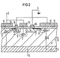
- the symbols of the FET 1, 2 and 3 are shown in the sectional view according to FIG. 2 for explanation.
- the semiconductor arrangement is arranged on a substrate 4 which, for. B. consists of an n + -doped zone 5 and an n - doped layer 6.
- the latter can be an epitaxial layer, for example.
- Two P-type zones 7 and 9 are embedded in the surface of the layer 6. Zones 7 and 9 form the drain zone and the source zone of FET 3. This is a lateral p-channel FET.
- N + -doped zones 8 and 10 are embedded in zones 7, 9. These are the source zones for the first vertical FET 1 and the second vertical FET 2. Zones 7, 9 also form the gate zones for FET 1 and 2.
- Zones 7, 8 and 9, 10 are each electrically connected to one another by a contact 16, 15.
- the surface of the substrate 4 is except for those places where the contacts 15 and 16 sit with an insulating layer 11, for. B. made of silicon dioxide.
- a gate electrode 12 is arranged on the layer 11 and covers the part of the gate zone 7 lying between the source zone 8 and zone 6.
- the gate electrode 12 is assigned to the FET 1.
- Two further gate electrodes 13, 14 are assigned to FET 3 and 2, respectively.
- FET 3 is a p-channel lateral FET, while FET 2 and FET 1 are n-channel vertical FET. FET 2 and 3 can be produced simultaneously with FET 1 without additional process steps by creating the two additional zones 9 and 10. To achieve a low channel resistance of the FET 3, the zones 7 and 9 have a small distance of z. B. 10 to 20 pm. The width of its channel should be as large as possible for the same reason.
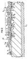
- the FET 2 and 3 forming the preamplifier of the semiconductor arrangement are preferably arranged on the edge of the substrate. Such an arrangement is shown in FIG. 3.
- the same parts as in Fig. 2 are given the same reference numerals here.
- the substrate 4 has a large number of first MISFETs, only a few of which are shown here. They have gate zones 18, 19 in which source zones 20, 21 are embedded. These first MISFETs are connected in parallel by a metal layer 17.
- Each of the first MISFETs has a gate electrode, only one of which is shown here and is designated by 22.
- the gate extrode 22 is electrically connected to any further gate electrodes and to the gate electrode 12. All gate electrodes are electrically connected to zones 9, 10 via contact 15.
- the control electrode 14 lying between the vertical MISFET 2 and the edge of the substrate 4 can be at a greater distance from the edge of the surface of the substrate than above the gate zone 9. This measure, together with a channel stopper 22 located at the edge and an auxiliary electrode 23 overlapping the gate electrode 14 and electrically separated from it by the insulating layer 11, serves to better distribute the edge field strength on the surface of the substrate.
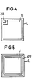
- the MISFET 2, 3 of the input amplifier can, as shown in FIG. 3, be arranged on the edge of the substrate. As shown in FIG. 4, the FET 2, 3 can be arranged within an area of the substrate 4 that is recessed from the main FET 1. However, it is also possible to design the preamplifier FET 2, 3 in a ring and to arrange them between the edge of the substrate 4 and the TEL 1. 4 and 5, a greatly simplified representation has been chosen which does not take into account the actual fine structure of FET 1, 2 and 3.
- the invention is e.g. B. for high-voltage MISFET with a reverse voltage z. B. usable from 500 V.
Landscapes
- Metal-Oxide And Bipolar Metal-Oxide Semiconductor Integrated Circuits (AREA)
- Junction Field-Effect Transistors (AREA)
Description
- Die Erfindung bezieht sich auf eine Halbleiteranordnung mit einem Substrat, in dem ein erster Vertikal-MISFET vom ersten Kanaltyp mit einer an der Oberfläche des Substrats liegenden Sourcezone, einer Gatezone und einer Gateelektrode enthalten ist, dessen Drainzone durch das Substrat gebildet ist.
- Vertikal-MISFET dieser Art eignen sich für Leistungsanwendungen und sind beispielsweise in der DE-OS-2 703 877 beschrieben worden. Bei einer Direktansteuerung z: B. durch IC's zeigt sich, daß sie wegen ihrer hohen Eingangskapazität nur relativ langsam eingeschaltet werden. Die Schaltgeschwindigkeit könnte durch äußere Treiberschaltungen erhöht werden. Das bedeutet jedoch einen zusätzlichen Aufwand.
- Der Erfindung liegt die Aufgabe zugrunde, eine Halbleiteranordnung der obengenannten Gattung derart weiterzubilden, daß die Schaltgeschwindigkeit auch bei geringer Eingangsleistung ohne zusätzlichen Aufwand erhöht wird.
- Diese Aufgabe wird gelöst durch die folgenden Merkmale:
- a) Das Substrat enthält einen weiteren Vertikal-MISFET vom ersten Kanaltyp mit einer an der Oberfläche des Substrats liegenden Sourcezone, einer Gatezone und einer Gateelektrode, dessen Drainzone durch das Substrat gebildet ist,
- b) das Substrat enthält einen Lateral-MISFET vom zweiten Kanaltyp mit einer an der Oberfläche des Substrats liegenden Sourcezone und einer an der Oberfläche des Substrats liegenden Drainzone,
- c) die Sourcezonen des weiteren Vertikal-MISFET und des Lateral-MISFET sind elektrisch miteinander und mit der Gateelektrode des ersten Vertikal-MISFET verbunden,
- d) die Gateelektroden des Lateral-MISFET und des weiteren Vertikal-MISFET sind elektrisch miteinander verbunden,
- e) die Drainzone des Lateral-MISFET ist elektrisch mit der Sourcezone des ersten Vertikal-MISFET verbunden.
- Weiterbildungen der Erfindung sind Gegenstand der Unteransprüche.
- Die Erfindung wird anhand einiger Ausführungsbeispiele in Verbindung mit den Fig. 1 bis 5 näher erläutert. Es zeigen:
- Fig. 1 ein Ersatzschaltbild der Halbleiteranordnung gemäß der Erfindung,
- Fig. 2 einen Schnitt durch eine prinzipielle Ausführungsform,
- Fig. 3 einen Schnitt durch ein Ausführungsbeispiel,
- Fig. 4 und 5 die Aufsichten auf zwei Ausführungsbeispiele mit verschiedenen Zuordnungen der Teile der Halbleiteranordnung.
- Im Ersatzschaltbild nach Fig. 1 ist der Leistungs-MISFET mit 1 bezeichnet. Er weist drainseitig einen Widerstand R auf, der den Bahnwiderstand des Substrats darstellt. Drainseitig liegt der FET 1 mit der Klemme D über den Widerstand R und eine Last L an einer Spannung +U. Sourceseitig liegt er über die Klemme 5 beispielsweise auf Massepotential. Dem FET 1 und seinem Bahnwiderstand ist die Reihenschaltung bestehend aus einem zweiten MISFET 2 vom gleichen Kanaltyp und einem dritten MISFET 3 vom entgegengesetzten Kanaltyp parallelgeschaltet. Die MISFET 1 und 2 sind als n-Kanal-MISFET dargestellt, während der MISFET 3 vom p-Kanaltyp ist. Die Sourcezonen der MISFET 2 und 3 sind einerseits elektrisch miteinander verbunden und andererseits mit der Gateelektrode des MISFET 1. Die Gateelektroden der MISFET 2 und 3 sind elektrisch miteinander verbunden und bilden einen Gateanschluß G. Die MISFET und 3 bilden einen Vorverstärker für den MISFET 1. Zur Erläuterung der Funktion wurde die Gate-Source-Kapazität CGS des ersten MISFET 1 eingezeichnet.
- Wird an den Gateanschluß G eine Signalspannung uE der gezeigten Form angelegt, so wird der zweite FET 2 leitend gesteuert und an der Gateelektrode des FET 1 erscheint eine positive Spannung. Diese lädt die Kapazität CGS auf und der FET 1 wird eingeschaltet. Wird die Eingangsspannung uE wieder Null, so bleibt die Gate-Source-Spannung am FET 1, bedingt durch die Ladung in CGS, zunächst positiv. Damit wird das Potential der Sourcezone des FET 3 gegenüber seinem Gatepotential positiv und der FET 3 wird leitend. Damit wird die Kapazität CGs schnell entladen und der FET 1 wird gesperrt.
- In die Schnittdarstellung nach Fig. 2 sind die Symbole der FET 1, 2 und 3 zur Erläuterung eingezeichnet. Die Halbleiteranordnung ist auf einem Substrat 4 angeordnet, das z. B. aus einer n+-dotierten Zone 5 und einer n--dotierten Schicht 6 besteht. Letztere kann beispielsweise eine Epitaxieschicht sein. In die Oberfläche der Schicht 6 sind zwei P-leitende Zonen 7 und 9 eingebettet. Die Zonen 7 und 9 bilden die Drainzone bzw. die Sourcezone des FET 3. Dieser ist ein lateraler p-Kanal-FET. In den Zonen 7, 9 sind n+-dotierte Zonen 8 bzw. 10 eingebettet. Diese sind die Sourcezonen für den ersten Vertikal-FET 1 bzw. den zweiten Vertikal-FET 2. Die Zonen 7, 9 bilden auch die Gatezonen für die FET 1 bzw. 2. Diese Anordnung ist besonders platzsparend; die Kanalzonen der FET 1 und 2 könnten jedoch auch von der Source- und Drainzone des FET 3 räumlich getrennt sein. Die Zonen 7, 8 und 9, 10 sind durch je einen Kontakt 16, 15 elektrisch miteinander verbunden. Die Oberfläche des Substrats 4 ist bis auf diejenigen Stellen, wo die Kontakte 15 und 16 sitzen, mit einer Isolierschicht 11, z. B. aus Siliciumdioxid, bedeckt. Auf der Schicht 11 ist eine Gateelektrode 12 angeordnet, die den zwischen Sourcezone 8 und Zone 6 liegenden Teil der Gatezone 7 überdeckt. Die Gateelektrode 12 ist den FET 1 zugeordnet. Zwei weitere Gateelektroden 13, 14 sind den FET 3 bzw. 2 zugeordnet.
- Der FET 3 ist ein p-Kanal-Lateral-FET, während FET 2 und FET 1 n-Kanal-Vertikal-FET sind. Die FET 2 und 3 lassen sich gleichzeitig mit dem FET 1 ohne zusätzliche Verfahrensschritte durch die Erzeugung der beiden zusätzlichen Zonen 9 und 10 herstellen. Zur Erzielung eines niedrigen Kanalwiderstands des FET 3 haben die Zonen 7 und 9 einen geringen Abstand von z. B. 10 bis 20 pm. Die Breite seines Kanals soll aus dem gleichen Grund möglichst groß sein.
- Die den Vorverstärker der Halbleiteranordnung bildenden FET 2 und 3 werden vorzugsweise am Rand des Substrats angeordnet. Eine solche Anordnung ist in Fig. 3 dargestellt. Gleiche Teile wie in Fig. 2 sind hier mit gleichen Bezugszeichen versehen. Das Substrat 4 weist eine Vielzahl von ersten MISFET auf, von denen hier nur einige dargestellt sind. Sie haben Gatezonen 18, 19, in die Sourcezonen 20, 21 eingebettet sind. Diese ersten MISFET sind durch eine Metallschicht 17 einander parallelgeschaltet. Zu jeden der ersten MISFET gehört eine Gateelektrode, von denen hier nur eine weitere dargestellt und mit 22 bezeichnet ist. Die Gateelextrode 22 ist mit eventuellen weiteren Gateelektroden und mit der Gateelektrode 12 elektrisch verbunden. Alle Gateelektroden sind über den Kontakt 15 elektrisch mit den Zonen 9, 10 verbunden.
- Die zwischen dem Vertikal-MISFET 2 und dem Rand des Substrats 4 liegende Steuerelektrode 14 kann zum Rand hin einen größeren Abstand zur Oberfläche des Substrats als über der Gatezone 9 aufweisen. Diese Maßnahme dient zusammen mit einem am Rand sitzenden Channel-Stopper 22 und einer die Gateelektrode 14 überlappenden und elektrisch durch die Isolierschicht 11 von ihr getrennten Hilfselektrode 23 einer besseren Verteilung der Randfeldstärke an der Oberfläche des Substrats.
- Die MISFET 2, 3 des Eingangsverstärkers können, wie in Fig 3 dargestellt, an Rand des Substrats angeordnet sein. Wie in Fig. 4 gezeigt, können die FET 2, 3 dabei innerhalb einer von den Haupt-FET 1 ausgesparten Fläche des Substrats 4 angeordnet sein. Es ist jedoch auch möglich, die Vorverstärker-FET 2, 3 ringförmig auszubilden und zwischen dem Rand des Substrats 4 und dem TEL 1 anzuordnen. In Fig. 4 und 5 wurde dabei eine stark vereinfachte Darstellung gewählt, die die tatsächliche Feinstruktur der FET 1, 2 und 3 außer Betracht läßt.
- Die Erfindung ist z. B. für Hochvolt-MISFET mit einer Sperrspannung z. B. ab 500 V brauchbar.
Claims (6)
Applications Claiming Priority (2)
| Application Number | Priority Date | Filing Date | Title |
|---|---|---|---|
| DE3301648 | 1983-01-19 | ||
| DE19833301648 DE3301648A1 (de) | 1983-01-19 | 1983-01-19 | Misfet mit eingangsverstaerker |
Publications (3)
| Publication Number | Publication Date |
|---|---|
| EP0114371A2 EP0114371A2 (de) | 1984-08-01 |
| EP0114371A3 EP0114371A3 (en) | 1986-03-12 |
| EP0114371B1 true EP0114371B1 (de) | 1989-03-08 |
Family
ID=6188643
Family Applications (1)
| Application Number | Title | Priority Date | Filing Date |
|---|---|---|---|
| EP83112934A Expired EP0114371B1 (de) | 1983-01-19 | 1983-12-21 | MISFET mit Eingangsverstärker |
Country Status (4)
| Country | Link |
|---|---|
| US (1) | US4631565A (de) |
| EP (1) | EP0114371B1 (de) |
| JP (1) | JPS59138364A (de) |
| DE (2) | DE3301648A1 (de) |
Families Citing this family (60)
| Publication number | Priority date | Publication date | Assignee | Title |
|---|---|---|---|---|
| US4712124A (en) * | 1986-12-22 | 1987-12-08 | North American Philips Corporation | Complementary lateral insulated gate rectifiers with matched "on" resistances |
| DE19546562C1 (de) * | 1995-12-13 | 1997-04-03 | Leica Ag | Schaltungsanordnung zur Ansteuerung einer Impulsendstufe |
| EP0936674B1 (de) * | 1998-02-10 | 2006-04-26 | STMicroelectronics S.r.l. | Integrierte Schaltung mit einem VDMOS-Transistor, der gegen Überspannungen zwischen Source und Gate geschützt ist |
| JP2001094094A (ja) * | 1999-09-21 | 2001-04-06 | Hitachi Ltd | 半導体装置およびその製造方法 |
| JP2002217416A (ja) * | 2001-01-16 | 2002-08-02 | Hitachi Ltd | 半導体装置 |
| WO2002097888A1 (en) * | 2001-05-25 | 2002-12-05 | Mitsubishi Denki Kabushiki Kaisha | Power semiconductor device |
| US8067855B2 (en) * | 2003-05-06 | 2011-11-29 | Enecsys Limited | Power supply circuits |
| EP1623495B1 (de) | 2003-05-06 | 2009-10-07 | Enecsys Limited | Stromversorgungsschaltungen |
| GB2421847B (en) * | 2004-11-08 | 2006-12-27 | Enecsys Ltd | Integrated circuits |
| US11881814B2 (en) | 2005-12-05 | 2024-01-23 | Solaredge Technologies Ltd. | Testing of a photovoltaic panel |
| US10693415B2 (en) | 2007-12-05 | 2020-06-23 | Solaredge Technologies Ltd. | Testing of a photovoltaic panel |
| GB2440974B (en) * | 2006-08-04 | 2011-06-01 | Zetex Semiconductors Plc | Power supply circuit |
| US8816535B2 (en) | 2007-10-10 | 2014-08-26 | Solaredge Technologies, Ltd. | System and method for protection during inverter shutdown in distributed power installations |
| US11296650B2 (en) | 2006-12-06 | 2022-04-05 | Solaredge Technologies Ltd. | System and method for protection during inverter shutdown in distributed power installations |
| US8618692B2 (en) | 2007-12-04 | 2013-12-31 | Solaredge Technologies Ltd. | Distributed power system using direct current power sources |
| US11309832B2 (en) | 2006-12-06 | 2022-04-19 | Solaredge Technologies Ltd. | Distributed power harvesting systems using DC power sources |
| US11888387B2 (en) | 2006-12-06 | 2024-01-30 | Solaredge Technologies Ltd. | Safety mechanisms, wake up and shutdown methods in distributed power installations |
| US12316274B2 (en) | 2006-12-06 | 2025-05-27 | Solaredge Technologies Ltd. | Pairing of components in a direct current distributed power generation system |
| US9112379B2 (en) | 2006-12-06 | 2015-08-18 | Solaredge Technologies Ltd. | Pairing of components in a direct current distributed power generation system |
| US11569659B2 (en) | 2006-12-06 | 2023-01-31 | Solaredge Technologies Ltd. | Distributed power harvesting systems using DC power sources |
| US11855231B2 (en) | 2006-12-06 | 2023-12-26 | Solaredge Technologies Ltd. | Distributed power harvesting systems using DC power sources |
| US8319483B2 (en) | 2007-08-06 | 2012-11-27 | Solaredge Technologies Ltd. | Digital average input current control in power converter |
| US11687112B2 (en) | 2006-12-06 | 2023-06-27 | Solaredge Technologies Ltd. | Distributed power harvesting systems using DC power sources |
| US11735910B2 (en) | 2006-12-06 | 2023-08-22 | Solaredge Technologies Ltd. | Distributed power system using direct current power sources |
| US8963369B2 (en) | 2007-12-04 | 2015-02-24 | Solaredge Technologies Ltd. | Distributed power harvesting systems using DC power sources |
| US8384243B2 (en) | 2007-12-04 | 2013-02-26 | Solaredge Technologies Ltd. | Distributed power harvesting systems using DC power sources |
| US8947194B2 (en) | 2009-05-26 | 2015-02-03 | Solaredge Technologies Ltd. | Theft detection and prevention in a power generation system |
| US9088178B2 (en) | 2006-12-06 | 2015-07-21 | Solaredge Technologies Ltd | Distributed power harvesting systems using DC power sources |
| US8319471B2 (en) | 2006-12-06 | 2012-11-27 | Solaredge, Ltd. | Battery power delivery module |
| US9130401B2 (en) | 2006-12-06 | 2015-09-08 | Solaredge Technologies Ltd. | Distributed power harvesting systems using DC power sources |
| US8013472B2 (en) | 2006-12-06 | 2011-09-06 | Solaredge, Ltd. | Method for distributed power harvesting using DC power sources |
| US8473250B2 (en) | 2006-12-06 | 2013-06-25 | Solaredge, Ltd. | Monitoring of distributed power harvesting systems using DC power sources |
| EP3496258B1 (de) | 2007-12-05 | 2025-02-05 | Solaredge Technologies Ltd. | Sicherheitsmechanismus in verteilten strominstallationen |
| US8049523B2 (en) | 2007-12-05 | 2011-11-01 | Solaredge Technologies Ltd. | Current sensing on a MOSFET |
| US11264947B2 (en) | 2007-12-05 | 2022-03-01 | Solaredge Technologies Ltd. | Testing of a photovoltaic panel |
| WO2009072075A2 (en) | 2007-12-05 | 2009-06-11 | Solaredge Technologies Ltd. | Photovoltaic system power tracking method |
| EP2232690B1 (de) | 2007-12-05 | 2016-08-31 | Solaredge Technologies Ltd. | Parallel geschaltete umrichter |
| EP4145691A1 (de) | 2008-03-24 | 2023-03-08 | Solaredge Technologies Ltd. | Schaltwandler mit einem hilfskommutierungsschaltkreis zur nullstromschaltung |
| EP3121922B1 (de) | 2008-05-05 | 2020-03-04 | Solaredge Technologies Ltd. | Gleichstromleistungskombinierer |
| US12418177B2 (en) | 2009-10-24 | 2025-09-16 | Solaredge Technologies Ltd. | Distributed power system using direct current power sources |
| US10673222B2 (en) | 2010-11-09 | 2020-06-02 | Solaredge Technologies Ltd. | Arc detection and prevention in a power generation system |
| US10230310B2 (en) | 2016-04-05 | 2019-03-12 | Solaredge Technologies Ltd | Safety switch for photovoltaic systems |
| US10673229B2 (en) | 2010-11-09 | 2020-06-02 | Solaredge Technologies Ltd. | Arc detection and prevention in a power generation system |
| GB2485527B (en) | 2010-11-09 | 2012-12-19 | Solaredge Technologies Ltd | Arc detection and prevention in a power generation system |
| GB2486408A (en) | 2010-12-09 | 2012-06-20 | Solaredge Technologies Ltd | Disconnection of a string carrying direct current |
| GB2483317B (en) | 2011-01-12 | 2012-08-22 | Solaredge Technologies Ltd | Serially connected inverters |
| US8570005B2 (en) | 2011-09-12 | 2013-10-29 | Solaredge Technologies Ltd. | Direct current link circuit |
| GB2498365A (en) | 2012-01-11 | 2013-07-17 | Solaredge Technologies Ltd | Photovoltaic module |
| GB2498791A (en) | 2012-01-30 | 2013-07-31 | Solaredge Technologies Ltd | Photovoltaic panel circuitry |
| GB2498790A (en) | 2012-01-30 | 2013-07-31 | Solaredge Technologies Ltd | Maximising power in a photovoltaic distributed power system |
| US9853565B2 (en) | 2012-01-30 | 2017-12-26 | Solaredge Technologies Ltd. | Maximized power in a photovoltaic distributed power system |
| GB2499991A (en) | 2012-03-05 | 2013-09-11 | Solaredge Technologies Ltd | DC link circuit for photovoltaic array |
| US10115841B2 (en) | 2012-06-04 | 2018-10-30 | Solaredge Technologies Ltd. | Integrated photovoltaic panel circuitry |
| US9941813B2 (en) | 2013-03-14 | 2018-04-10 | Solaredge Technologies Ltd. | High frequency multi-level inverter |
| US9548619B2 (en) | 2013-03-14 | 2017-01-17 | Solaredge Technologies Ltd. | Method and apparatus for storing and depleting energy |
| EP2779251B1 (de) | 2013-03-15 | 2019-02-27 | Solaredge Technologies Ltd. | Umgehungsmechanismus |
| US9318974B2 (en) | 2014-03-26 | 2016-04-19 | Solaredge Technologies Ltd. | Multi-level inverter with flying capacitor topology |
| US11177663B2 (en) | 2016-04-05 | 2021-11-16 | Solaredge Technologies Ltd. | Chain of power devices |
| US11018623B2 (en) | 2016-04-05 | 2021-05-25 | Solaredge Technologies Ltd. | Safety switch for photovoltaic systems |
| US12057807B2 (en) | 2016-04-05 | 2024-08-06 | Solaredge Technologies Ltd. | Chain of power devices |
Family Cites Families (9)
| Publication number | Priority date | Publication date | Assignee | Title |
|---|---|---|---|---|
| DE2703877C2 (de) * | 1977-01-31 | 1982-06-03 | Siemens Ag, 1000 Berlin Und 8000 Muenchen | MIS-Transistor von kurzer Kanallänge und Verfahren zu seiner Herstellung |
| US4199774A (en) * | 1978-09-18 | 1980-04-22 | The Board Of Trustees Of The Leland Stanford Junior University | Monolithic semiconductor switching device |
| US4455565A (en) * | 1980-02-22 | 1984-06-19 | Rca Corporation | Vertical MOSFET with an aligned gate electrode and aligned drain shield electrode |
| US4345265A (en) * | 1980-04-14 | 1982-08-17 | Supertex, Inc. | MOS Power transistor with improved high-voltage capability |
| DE3114971A1 (de) * | 1980-04-14 | 1982-01-14 | Supertex, Inc., 94086 Sunnyvale, Calif. | Dmos-halbleiterbauelement |
| US4402003A (en) * | 1981-01-12 | 1983-08-30 | Supertex, Inc. | Composite MOS/bipolar power device |
| FR2505102B1 (fr) * | 1981-04-29 | 1986-01-24 | Radiotechnique Compelec | Amplificateur de type darlington forme d'un transistor a effet de champ et d'un transistor bipolaire, et sa realisation en structure semi-conductrice integree |
| JPS57186833A (en) * | 1981-05-13 | 1982-11-17 | Hitachi Ltd | Switching element |
| US4541001A (en) * | 1982-09-23 | 1985-09-10 | Eaton Corporation | Bidirectional power FET with substrate-referenced shield |
-
1983
- 1983-01-19 DE DE19833301648 patent/DE3301648A1/de not_active Withdrawn
- 1983-12-02 US US06/557,712 patent/US4631565A/en not_active Expired - Fee Related
- 1983-12-21 DE DE8383112934T patent/DE3379365D1/de not_active Expired
- 1983-12-21 EP EP83112934A patent/EP0114371B1/de not_active Expired
-
1984
- 1984-01-19 JP JP59007907A patent/JPS59138364A/ja active Pending
Also Published As
| Publication number | Publication date |
|---|---|
| DE3301648A1 (de) | 1984-07-19 |
| EP0114371A2 (de) | 1984-08-01 |
| US4631565A (en) | 1986-12-23 |
| JPS59138364A (ja) | 1984-08-08 |
| EP0114371A3 (en) | 1986-03-12 |
| DE3379365D1 (en) | 1989-04-13 |
Similar Documents
| Publication | Publication Date | Title |
|---|---|---|
| EP0114371B1 (de) | MISFET mit Eingangsverstärker | |
| EP0239862B1 (de) | Ansteuerschaltung für einen Leistungs-MOSFET mit sourceseitiger Last | |
| DE2009102C3 (de) | Integrierte Halbleiteranordnung mit komplementären Feldeffekttransistoren | |
| DE102013213734B4 (de) | Strom-Sense-Transistor mit Einbettung von Sense-Transistorzellen und Verfahren zur Herstellung | |
| DE2706623C2 (de) | ||
| EP0236967B1 (de) | Schaltungsanordnung zum Ansteuern eines mit sourceseitiger Last verbundenen Mosfet | |
| EP0050773A2 (de) | Steuerbares MIS-Bauelement | |
| DE2740203C2 (de) | Ladungsgekoppelte Halbleiteranordnung | |
| DE19735425A1 (de) | Mosfet | |
| DE3326423A1 (de) | Integrierter schaltkreis | |
| DE2158270C3 (de) | Kontaktloser Schalter mit einem Feldeffekt-Thyristor | |
| DE1906324C3 (de) | Integrierte Halbleiteranordnung mit vier auf dem gleichen Halbleitersubstrat angeordneten und elektrisch miteinander verbundenen Feldeffekttransistorelementen | |
| DE2653484A1 (de) | Integrierbarer konstantwiderstand | |
| DE2451364C2 (de) | Digital steuerbarer MOS-Feldeffektkondensator | |
| EP0044021B1 (de) | Aus MIS-Feldeffekttransistoren bestehender elektrischer Widerstand für integrierte Halbleiterschaltungen | |
| DE2728532A1 (de) | Sperrschicht-feldeffekttransistor | |
| WO2005076366A2 (de) | Soi-halbleiterbauelement mit erhöhter spannungsfestigkeit | |
| DE2830437A1 (de) | Ladungsgekoppeltes filter | |
| EP0089527A2 (de) | Monolithisch integrierte Darlingtonschaltung | |
| EP0156022A2 (de) | Durch Feldeffekt steuerbares Halbleiterbauelement | |
| EP1285483A1 (de) | Halbleiter-bauelement | |
| DE102006048625B4 (de) | Halbleiterbauelement | |
| DE102016109971B3 (de) | Spinning-current-verfahren für magfet-sensor | |
| DE2105479A1 (de) | Schaltung und Aufbau eines Halbleiterspeicherelementes | |
| CH683388A5 (de) | Anordnung zur Eigenschaftsverbesserung von mit P/N-Uebergängen versehenen Halbleiterstrukturen. |
Legal Events
| Date | Code | Title | Description |
|---|---|---|---|
| PUAI | Public reference made under article 153(3) epc to a published international application that has entered the european phase |
Free format text: ORIGINAL CODE: 0009012 |
|
| AK | Designated contracting states |
Designated state(s): CH DE FR GB IT LI |
|
| 17P | Request for examination filed |
Effective date: 19841221 |
|
| PUAL | Search report despatched |
Free format text: ORIGINAL CODE: 0009013 |
|
| AK | Designated contracting states |
Kind code of ref document: A3 Designated state(s): CH DE FR GB IT LI |
|
| 17Q | First examination report despatched |
Effective date: 19880316 |
|
| GRAA | (expected) grant |
Free format text: ORIGINAL CODE: 0009210 |
|
| AK | Designated contracting states |
Kind code of ref document: B1 Designated state(s): CH DE FR GB IT LI |
|
| REF | Corresponds to: |
Ref document number: 3379365 Country of ref document: DE Date of ref document: 19890413 |
|
| ITF | It: translation for a ep patent filed | ||
| GBT | Gb: translation of ep patent filed (gb section 77(6)(a)/1977) | ||
| ET | Fr: translation filed | ||
| PLBE | No opposition filed within time limit |
Free format text: ORIGINAL CODE: 0009261 |
|
| STAA | Information on the status of an ep patent application or granted ep patent |
Free format text: STATUS: NO OPPOSITION FILED WITHIN TIME LIMIT |
|
| 26N | No opposition filed | ||
| PGFP | Annual fee paid to national office [announced via postgrant information from national office to epo] |
Ref country code: CH Payment date: 19900323 Year of fee payment: 7 |
|
| PGFP | Annual fee paid to national office [announced via postgrant information from national office to epo] |
Ref country code: GB Payment date: 19901116 Year of fee payment: 8 |
|
| PGFP | Annual fee paid to national office [announced via postgrant information from national office to epo] |
Ref country code: FR Payment date: 19901219 Year of fee payment: 8 |
|
| ITTA | It: last paid annual fee | ||
| PG25 | Lapsed in a contracting state [announced via postgrant information from national office to epo] |
Ref country code: LI Effective date: 19901231 Ref country code: CH Effective date: 19901231 |
|
| PGFP | Annual fee paid to national office [announced via postgrant information from national office to epo] |
Ref country code: DE Payment date: 19910225 Year of fee payment: 8 |
|
| REG | Reference to a national code |
Ref country code: CH Ref legal event code: PL |
|
| PG25 | Lapsed in a contracting state [announced via postgrant information from national office to epo] |
Ref country code: GB Effective date: 19911221 |
|
| GBPC | Gb: european patent ceased through non-payment of renewal fee | ||
| PG25 | Lapsed in a contracting state [announced via postgrant information from national office to epo] |
Ref country code: FR Effective date: 19920831 |
|
| PG25 | Lapsed in a contracting state [announced via postgrant information from national office to epo] |
Ref country code: DE Effective date: 19920901 |
|
| REG | Reference to a national code |
Ref country code: FR Ref legal event code: ST |