EP0114493A1 - Cellule photo-électrochimique - Google Patents
Cellule photo-électrochimique Download PDFInfo
- Publication number
- EP0114493A1 EP0114493A1 EP83307731A EP83307731A EP0114493A1 EP 0114493 A1 EP0114493 A1 EP 0114493A1 EP 83307731 A EP83307731 A EP 83307731A EP 83307731 A EP83307731 A EP 83307731A EP 0114493 A1 EP0114493 A1 EP 0114493A1
- Authority
- EP
- European Patent Office
- Prior art keywords
- semiconductor
- cell according
- cell
- solvent
- solution
- Prior art date
- Legal status (The legal status is an assumption and is not a legal conclusion. Google has not performed a legal analysis and makes no representation as to the accuracy of the status listed.)
- Withdrawn
Links
- 239000002904 solvent Substances 0.000 claims abstract description 40
- 239000007788 liquid Substances 0.000 claims abstract description 36
- 239000003792 electrolyte Substances 0.000 claims abstract description 30
- 238000006243 chemical reaction Methods 0.000 claims abstract description 19
- 239000004065 semiconductor Substances 0.000 claims description 79
- OKKJLVBELUTLKV-UHFFFAOYSA-N Methanol Chemical group OC OKKJLVBELUTLKV-UHFFFAOYSA-N 0.000 claims description 45
- WEVYAHXRMPXWCK-UHFFFAOYSA-N Acetonitrile Chemical compound CC#N WEVYAHXRMPXWCK-UHFFFAOYSA-N 0.000 claims description 30
- 229910001868 water Inorganic materials 0.000 claims description 22
- 229910052710 silicon Inorganic materials 0.000 claims description 21
- 239000010703 silicon Substances 0.000 claims description 21
- XUIMIQQOPSSXEZ-UHFFFAOYSA-N Silicon Chemical group [Si] XUIMIQQOPSSXEZ-UHFFFAOYSA-N 0.000 claims description 17
- XLYOFNOQVPJJNP-UHFFFAOYSA-N water Substances O XLYOFNOQVPJJNP-UHFFFAOYSA-N 0.000 claims description 17
- 229910001218 Gallium arsenide Inorganic materials 0.000 claims description 15
- JBRZTFJDHDCESZ-UHFFFAOYSA-N AsGa Chemical compound [As]#[Ga] JBRZTFJDHDCESZ-UHFFFAOYSA-N 0.000 claims description 9
- 230000004907 flux Effects 0.000 claims description 9
- MHCFAGZWMAWTNR-UHFFFAOYSA-M lithium perchlorate Chemical group [Li+].[O-]Cl(=O)(=O)=O MHCFAGZWMAWTNR-UHFFFAOYSA-M 0.000 claims description 9
- 229910001486 lithium perchlorate Inorganic materials 0.000 claims description 9
- 239000000758 substrate Substances 0.000 claims description 7
- KTWOOEGAPBSYNW-UHFFFAOYSA-N ferrocene Chemical group [Fe+2].C=1C=C[CH-]C=1.C=1C=C[CH-]C=1 KTWOOEGAPBSYNW-UHFFFAOYSA-N 0.000 claims description 6
- -1 (1-hydroxyethyl)ferrocenium salt Chemical class 0.000 claims description 5
- 125000004432 carbon atom Chemical group C* 0.000 claims description 4
- 230000005855 radiation Effects 0.000 claims description 4
- MARUHZGHZWCEQU-UHFFFAOYSA-N 5-phenyl-2h-tetrazole Chemical compound C1=CC=CC=C1C1=NNN=N1 MARUHZGHZWCEQU-UHFFFAOYSA-N 0.000 claims description 3
- BOXSCYUXSBYGRD-UHFFFAOYSA-N cyclopenta-1,3-diene;iron(3+) Chemical class [Fe+3].C=1C=C[CH-]C=1.C=1C=C[CH-]C=1 BOXSCYUXSBYGRD-UHFFFAOYSA-N 0.000 claims description 3
- 230000005611 electricity Effects 0.000 claims description 3
- CBXCPBUEXACCNR-UHFFFAOYSA-N tetraethylammonium Chemical group CC[N+](CC)(CC)CC CBXCPBUEXACCNR-UHFFFAOYSA-N 0.000 claims description 3
- GPXJNWSHGFTCBW-UHFFFAOYSA-N Indium phosphide Chemical compound [In]#P GPXJNWSHGFTCBW-UHFFFAOYSA-N 0.000 claims description 2
- UHYPYGJEEGLRJD-UHFFFAOYSA-N cadmium(2+);selenium(2-) Chemical compound [Se-2].[Cd+2] UHYPYGJEEGLRJD-UHFFFAOYSA-N 0.000 claims description 2
- YDZCBKCOBVVHFT-UHFFFAOYSA-N cyclopenta-1,3-diene;1-cyclopenta-1,3-dien-1-ylethanol;iron(2+) Chemical group [Fe+2].C=1C=C[CH-]C=1.CC(O)C1=CC=C[CH-]1 YDZCBKCOBVVHFT-UHFFFAOYSA-N 0.000 claims description 2
- 150000002825 nitriles Chemical class 0.000 claims description 2
- 239000003795 chemical substances by application Substances 0.000 claims 2
- 150000001875 compounds Chemical class 0.000 claims 1
- 125000005207 tetraalkylammonium group Chemical group 0.000 claims 1
- 239000007791 liquid phase Substances 0.000 abstract description 2
- 239000000243 solution Substances 0.000 description 50
- 239000000523 sample Substances 0.000 description 15
- 239000011521 glass Substances 0.000 description 14
- 229910021417 amorphous silicon Inorganic materials 0.000 description 9
- 239000013078 crystal Substances 0.000 description 9
- 239000000463 material Substances 0.000 description 9
- 230000004888 barrier function Effects 0.000 description 7
- IJGRMHOSHXDMSA-UHFFFAOYSA-N Atomic nitrogen Chemical compound N#N IJGRMHOSHXDMSA-UHFFFAOYSA-N 0.000 description 6
- 239000004593 Epoxy Substances 0.000 description 6
- 238000000034 method Methods 0.000 description 6
- BASFCYQUMIYNBI-UHFFFAOYSA-N platinum Chemical compound [Pt] BASFCYQUMIYNBI-UHFFFAOYSA-N 0.000 description 6
- 238000009792 diffusion process Methods 0.000 description 5
- 238000010521 absorption reaction Methods 0.000 description 4
- 238000010586 diagram Methods 0.000 description 4
- 229910052736 halogen Inorganic materials 0.000 description 4
- 238000010907 mechanical stirring Methods 0.000 description 4
- 238000010791 quenching Methods 0.000 description 4
- 239000007787 solid Substances 0.000 description 4
- 238000003756 stirring Methods 0.000 description 4
- 239000000126 substance Substances 0.000 description 4
- 238000012546 transfer Methods 0.000 description 4
- RYGMFSIKBFXOCR-UHFFFAOYSA-N Copper Chemical compound [Cu] RYGMFSIKBFXOCR-UHFFFAOYSA-N 0.000 description 3
- BQCADISMDOOEFD-UHFFFAOYSA-N Silver Chemical compound [Ag] BQCADISMDOOEFD-UHFFFAOYSA-N 0.000 description 3
- 230000015572 biosynthetic process Effects 0.000 description 3
- 238000005530 etching Methods 0.000 description 3
- 238000005286 illumination Methods 0.000 description 3
- 150000002500 ions Chemical class 0.000 description 3
- 229910021421 monocrystalline silicon Inorganic materials 0.000 description 3
- 229910052757 nitrogen Inorganic materials 0.000 description 3
- 230000009467 reduction Effects 0.000 description 3
- 230000027756 respiratory electron transport chain Effects 0.000 description 3
- 229910052709 silver Inorganic materials 0.000 description 3
- 239000004332 silver Substances 0.000 description 3
- 238000002835 absorbance Methods 0.000 description 2
- 125000003158 alcohol group Chemical group 0.000 description 2
- 229910052782 aluminium Inorganic materials 0.000 description 2
- XAGFODPZIPBFFR-UHFFFAOYSA-N aluminium Chemical compound [Al] XAGFODPZIPBFFR-UHFFFAOYSA-N 0.000 description 2
- 125000003277 amino group Chemical group 0.000 description 2
- 235000013405 beer Nutrition 0.000 description 2
- 239000013626 chemical specie Substances 0.000 description 2
- 238000007796 conventional method Methods 0.000 description 2
- 238000000354 decomposition reaction Methods 0.000 description 2
- 230000008021 deposition Effects 0.000 description 2
- ZOMNIUBKTOKEHS-UHFFFAOYSA-L dimercury dichloride Chemical class Cl[Hg][Hg]Cl ZOMNIUBKTOKEHS-UHFFFAOYSA-L 0.000 description 2
- 238000002848 electrochemical method Methods 0.000 description 2
- 230000005518 electrochemistry Effects 0.000 description 2
- 230000005496 eutectics Effects 0.000 description 2
- 238000001704 evaporation Methods 0.000 description 2
- 239000005337 ground glass Substances 0.000 description 2
- 230000006872 improvement Effects 0.000 description 2
- 239000004615 ingredient Substances 0.000 description 2
- 239000012212 insulator Substances 0.000 description 2
- 238000002161 passivation Methods 0.000 description 2
- 229920002120 photoresistant polymer Polymers 0.000 description 2
- 229910052697 platinum Inorganic materials 0.000 description 2
- 229910021420 polycrystalline silicon Inorganic materials 0.000 description 2
- 230000004044 response Effects 0.000 description 2
- 150000003839 salts Chemical class 0.000 description 2
- 230000003595 spectral effect Effects 0.000 description 2
- 229910001220 stainless steel Inorganic materials 0.000 description 2
- 239000010935 stainless steel Substances 0.000 description 2
- 125000001424 substituent group Chemical group 0.000 description 2
- 238000002834 transmittance Methods 0.000 description 2
- 229910052721 tungsten Inorganic materials 0.000 description 2
- 239000010937 tungsten Substances 0.000 description 2
- 235000012431 wafers Nutrition 0.000 description 2
- ZOXJGFHDIHLPTG-UHFFFAOYSA-N Boron Chemical compound [B] ZOXJGFHDIHLPTG-UHFFFAOYSA-N 0.000 description 1
- BNPJNOLDKSAJSD-UHFFFAOYSA-N C(C)[N+](CC)(CC)CC.[B+3] Chemical compound C(C)[N+](CC)(CC)CC.[B+3] BNPJNOLDKSAJSD-UHFFFAOYSA-N 0.000 description 1
- SCMDKDGVHDAFGO-UHFFFAOYSA-M Cl(=O)(=O)(=O)[O-].C1(C=CC=C1)[Co+]C1C=CC=C1 Chemical compound Cl(=O)(=O)(=O)[O-].C1(C=CC=C1)[Co+]C1C=CC=C1 SCMDKDGVHDAFGO-UHFFFAOYSA-M 0.000 description 1
- LFQSCWFLJHTTHZ-UHFFFAOYSA-N Ethanol Chemical compound CCO LFQSCWFLJHTTHZ-UHFFFAOYSA-N 0.000 description 1
- 206010022998 Irritability Diseases 0.000 description 1
- 229910010084 LiAlH4 Inorganic materials 0.000 description 1
- FYYHWMGAXLPEAU-UHFFFAOYSA-N Magnesium Chemical compound [Mg] FYYHWMGAXLPEAU-UHFFFAOYSA-N 0.000 description 1
- QAOWNCQODCNURD-UHFFFAOYSA-N Sulfuric acid Chemical compound OS(O)(=O)=O QAOWNCQODCNURD-UHFFFAOYSA-N 0.000 description 1
- 229920004482 WACKER® Polymers 0.000 description 1
- SPAHBIMNXMGCMI-UHFFFAOYSA-N [Ga].[In] Chemical compound [Ga].[In] SPAHBIMNXMGCMI-UHFFFAOYSA-N 0.000 description 1
- 238000013019 agitation Methods 0.000 description 1
- 150000001408 amides Chemical class 0.000 description 1
- 238000004458 analytical method Methods 0.000 description 1
- 238000000137 annealing Methods 0.000 description 1
- QVGXLLKOCUKJST-UHFFFAOYSA-N atomic oxygen Chemical compound [O] QVGXLLKOCUKJST-UHFFFAOYSA-N 0.000 description 1
- 238000005452 bending Methods 0.000 description 1
- 230000008033 biological extinction Effects 0.000 description 1
- 230000005540 biological transmission Effects 0.000 description 1
- 229910052796 boron Inorganic materials 0.000 description 1
- 239000005388 borosilicate glass Substances 0.000 description 1
- 150000001735 carboxylic acids Chemical class 0.000 description 1
- 239000000969 carrier Substances 0.000 description 1
- 230000008859 change Effects 0.000 description 1
- 238000010351 charge transfer process Methods 0.000 description 1
- 239000003153 chemical reaction reagent Substances 0.000 description 1
- 239000003638 chemical reducing agent Substances 0.000 description 1
- 239000004020 conductor Substances 0.000 description 1
- 238000012937 correction Methods 0.000 description 1
- 230000007797 corrosion Effects 0.000 description 1
- 238000005260 corrosion Methods 0.000 description 1
- SPKJCVZOZISLEI-UHFFFAOYSA-N cyclopenta-1,3-diene;1-cyclopenta-1,3-dien-1-ylethanone;iron(2+) Chemical compound [Fe+2].C=1C=C[CH-]C=1.CC(=O)C1=CC=C[CH-]1 SPKJCVZOZISLEI-UHFFFAOYSA-N 0.000 description 1
- 239000002274 desiccant Substances 0.000 description 1
- 229910003460 diamond Inorganic materials 0.000 description 1
- 239000010432 diamond Substances 0.000 description 1
- 238000010494 dissociation reaction Methods 0.000 description 1
- 230000005593 dissociations Effects 0.000 description 1
- 239000002019 doping agent Substances 0.000 description 1
- 238000001035 drying Methods 0.000 description 1
- 230000000694 effects Effects 0.000 description 1
- 239000008151 electrolyte solution Substances 0.000 description 1
- 238000006056 electrooxidation reaction Methods 0.000 description 1
- 229920006333 epoxy cement Polymers 0.000 description 1
- 150000002148 esters Chemical class 0.000 description 1
- 230000008020 evaporation Effects 0.000 description 1
- 238000002474 experimental method Methods 0.000 description 1
- 230000004927 fusion Effects 0.000 description 1
- BHEPBYXIRTUNPN-UHFFFAOYSA-N hydridophosphorus(.) (triplet) Chemical compound [PH] BHEPBYXIRTUNPN-UHFFFAOYSA-N 0.000 description 1
- AMGQUBHHOARCQH-UHFFFAOYSA-N indium;oxotin Chemical compound [In].[Sn]=O AMGQUBHHOARCQH-UHFFFAOYSA-N 0.000 description 1
- 238000002347 injection Methods 0.000 description 1
- 239000007924 injection Substances 0.000 description 1
- 150000002576 ketones Chemical class 0.000 description 1
- 230000031700 light absorption Effects 0.000 description 1
- 239000006193 liquid solution Substances 0.000 description 1
- 239000012280 lithium aluminium hydride Substances 0.000 description 1
- SIBGTNDYBZZMHL-UHFFFAOYSA-M lithium;methanol;perchlorate Chemical compound [Li+].OC.[O-]Cl(=O)(=O)=O SIBGTNDYBZZMHL-UHFFFAOYSA-M 0.000 description 1
- 238000004519 manufacturing process Methods 0.000 description 1
- 230000000873 masking effect Effects 0.000 description 1
- 229910052751 metal Inorganic materials 0.000 description 1
- 239000002184 metal Substances 0.000 description 1
- 239000000203 mixture Substances 0.000 description 1
- 239000003960 organic solvent Substances 0.000 description 1
- 230000003647 oxidation Effects 0.000 description 1
- 238000007254 oxidation reaction Methods 0.000 description 1
- 229910052760 oxygen Inorganic materials 0.000 description 1
- 239000001301 oxygen Substances 0.000 description 1
- 239000003973 paint Substances 0.000 description 1
- 230000035515 penetration Effects 0.000 description 1
- 125000002467 phosphate group Chemical group [H]OP(=O)(O[H])O[*] 0.000 description 1
- 238000002360 preparation method Methods 0.000 description 1
- 230000008569 process Effects 0.000 description 1
- 125000001453 quaternary ammonium group Chemical group 0.000 description 1
- 150000003242 quaternary ammonium salts Chemical class 0.000 description 1
- 239000000376 reactant Substances 0.000 description 1
- 238000002310 reflectometry Methods 0.000 description 1
- 230000007561 response to light intensity Effects 0.000 description 1
- 238000000926 separation method Methods 0.000 description 1
- 238000005245 sintering Methods 0.000 description 1
- 238000000859 sublimation Methods 0.000 description 1
- 230000008022 sublimation Effects 0.000 description 1
- 238000004381 surface treatment Methods 0.000 description 1
- 239000012808 vapor phase Substances 0.000 description 1
Images



Classifications
-
- H—ELECTRICITY
- H01—ELECTRIC ELEMENTS
- H01M—PROCESSES OR MEANS, e.g. BATTERIES, FOR THE DIRECT CONVERSION OF CHEMICAL ENERGY INTO ELECTRICAL ENERGY
- H01M14/00—Electrochemical current or voltage generators not provided for in groups H01M6/00 - H01M12/00; Manufacture thereof
- H01M14/005—Photoelectrochemical storage cells
-
- H—ELECTRICITY
- H01—ELECTRIC ELEMENTS
- H01G—CAPACITORS; CAPACITORS, RECTIFIERS, DETECTORS, SWITCHING DEVICES, LIGHT-SENSITIVE OR TEMPERATURE-SENSITIVE DEVICES OF THE ELECTROLYTIC TYPE
- H01G9/00—Electrolytic capacitors, rectifiers, detectors, switching devices, light-sensitive or temperature-sensitive devices; Processes of their manufacture
- H01G9/20—Light-sensitive devices
Definitions
- the present invention relates to photoelectrochemical cells, and in particular, to nonaqueous liquid junction cells useful as solar cells.
- the width of this depletion region is related to the amount of band bending, the dopant density of the semiconductor and the dielectric constant of the semiconductor.
- the field created in the depletion region may be of a physical dimension such that it will be effective in separating photogenerated electron-hole pairs created by light absorption at the semiconductor-liquid interface. ,Therefore, if the semiconductor is an n-type, for example, photogenerated holes will be driven by the space charge field to the semiconductor surface toward the solid- liquid interface. The electrons will be driven into the bulk of the semiconductor.
- the holes will be consumed by electron donation from the electroactive species in the liquid (oxidation of the redox species), while the electrons can be withdrawn from the semiconductor, passed through a load, and reinjected into the liquid. If the injection of the electrons back into the liquid results by reduction of the redox species in the production of the same chemical species which was used to quench the photogenerated hole, then there will be no net chemical change in the liquid and the overall conversion will be light to electrical power.
- electrons may produce a different chemical species from that used to quench the photogenerated holes, in which case the cell may function as a battery in storing energy for later use.
- the present invention is directed to semiconductor liquid junction photoelectrochemical cells containing a nonaqueous solvent and an electrolyte which form an ionically con - ductive solution, and further containing a redox couple dissolved in the solution which is suitable to accept and donate electrons from and to the electrodes of the cell upon exposure of the cell by an external source of light.
- the redox couple should be present in an amount sufficient to sustain a predetermined current, and that the concentrations of the electrolyte and the redox couple in the solution must provide a small voltage drop compared to the output voltage.
- the efficiency of the photoelectrochemical cell may be improved by one or more of a combination of factors, including, minimization of the ohmic losses due to the liquid and solute components of the cell, and improvement of the mass and charge transfer processes at the solid liquid interface and in the solution.
- the holes are consumed by a solution reductant, resulting in the flow of current.
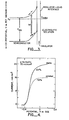
- the voltage difference between the energy at the edge of the semiconductor conduction band, E CB , and the redox potential, E Redox determines the barrier height of the cell.
- the band gap for semiconductor materials in solar cells is preferably 1.0 to 2.3 electron volts.
- the band diagram for an LIS junction is shown in FIG. 3. for an n-type semiconductor.
- the insulator region may be a limited thickness, deliberately formed oxide layer resulting from the limitation of the total water content of the solution. The presence of such an oxide insulator layer may improve the short circuit current, I sC , and open circuit voltage, Voc , of the cell by acting as a barrier to majority carriers.
- the formal analysis of an LIS structure is analogous to the solid state treatment of an MIS structure.
- the photoelectrochemical cells according to the present invention comprise a semiconductor photoactive electrode, a nonaqueous solvent containing a dissolved electrolyte forming an ionically conductive solution, an electrode providing an electrical connection from the solution to the photoactive electrode, and a redox couple dissolved in the solution which is suitable to accept and donate electrons from and to the electrodes upon exposure the cell by an external source of light, such as solar radiation.
- the solvent used in the liquid phase of the semiconductor liquid photoelectrochemical cells according to the present invention are nonaqueous.
- the nonaqueous solvent may be of the type which self-dissociates into solvent molecules which are ionically conductive or may be a solvent such that an electrolyte added thereto will be substantially dissociated to form an ionically conductive solution.
- the solvent it is preferable that the solvent have a relatively high dielectric constant in order to achieve substantial dissociation of the electrolyte.
- the solvent have a relatively low viscosity in order to facilitate mass transfer of the electrolyte ions through the liquid.
- preferred solvents should have dielectric constants greater than about 20 and viscosities less than about 2 centipoise.
- a preferred class of solvents comprises the alkanols of 1 to 6 carbon atoms, particularly methanol.
- a second preferred class of solvents comprises nitriles of 2 to 6 carbon atoms, particularly acetonitrile.
- the solvent will be a _ matter of choice within the-ordinary skill of those in the art, utilizing conventional tables of solvent viscosities and dielectric constants, such as, Experimental Electrochemistry for Chemists, Sawyer, Donald T., and Roberts, Julian L., Jr.,-John Willey & Sons, New York (1974), Chapter IV.
- n in a given volume of solution, V, to insure that there is insufficient water present to form an insulating oxide layer on a semiconductor may be calculated. If there are 10 16 molecules per centimeter square on the electrode surface, 0 formation of 40 A of oxide, or about 8 monolayers, would require 8 x 10 16 molecules of water per square centimeter of exposed electrode area. Assuming a rectangular geometry for the cell, either the thickness of the liquid, t, or the concentration of water, M, can be determined if the other is given, according to the following equation:
- This equation should be general for any given volume and geometry of cell. Since according to conventional methods, it is unlikely that the solvent could be dried of water below about .01 ppm (10 8 moles/liter or 6.02X 10 molecules per liter), this places an upper limit on the volume of the nonaqueous solvent permitted to be in contact with the semiconductor.
- the restricted amount of water present in the solvent may be arranged to be sufficient to form a limited amount of oxide to create an LIS junction as shown in Figure 3.
- the power output of a two-electrode LIS cell will not degrade substantially over time.
- an oxide layer in the range of 20-40 0 A is preferred for the LIS junction.
- the electrolytes utilized in accordance with the present invention should be of the nature which are substantially dissociated in the solvent to form an ionically conductive solution. Furthermore, the amount of electrolyte present is to be selected in an amount sufficient to provide no greater than a predetermined maximum electrical resistance due to the solution. The resistance of the nonaqueous solution, including the solutes dissolved therein, to current flow should be minimized in order to prevent large resistive losses. The electrolyte must therefore dissolve in the solvent and dissociate to yield conductive ions and must result in conductivities large enough to meet the resistivity spec'ifications at the given concentration.
- t where R is resistance and p is the resistivity in ohm-cm.
- R resistance
- p the resistivity in ohm-cm.
- IR the voltage loss due to any particular solution resistance
- a typical cell may have an output voltage of around 0.50 volts.
- a predetermined limit for IR losses due to the solution may be selected to be 10% or less. Therefore, if the voltage loss is 0.05V, and the current is 0.05 A/cm 2 R should be 1 ohm or less for a 1 cm 2 area.
- a preferred electrolyte according to the present invention is lithium perchlorate because of its solubility and conductivity.
- the preferred electrolytes are the quaternary ammonium salts, particularly quaternary ammonium borontetrafluoride salts.
- a preferred electrolyte is tetraethyl ammonium borontetrafluoride.
- the electroactive species, or redox couple, dissolved in the liquid in accordance with the present invention should have a redox potential such that it is suitable to accept and donate electrons from and to the electrodes in the cell upon exposure of the cell to an external source of light.
- the redox couple should be present in an amount sufficient to sustain a predetermined maximum current flux relative to the maximum photon flux of the incident light. Also, as a solute in the liquid, the redox couple should meet the limitations as to imparting no greater than a predetermined maximum electrical resistance due to the solution.
- the solution will present in the cell a thin layer, preferably having a thickness less than 100 microns, usually in the range of 10 to 100 microns.
- a cell having a thin solution layer is advantageous since the liquid volume between the electrodes is relatively small, therefore giving a higher permissible water concentration, wherein the limit of water present is determined as described above in connection with the formation of an LIS junction.
- the predetermined maximum permissible resistance of the solution may be satisfied by a thin layer, given that electrolyte conductivities are usually less than 100 mmho cm -1 .
- mechanical stirring of a thin layer is not required since natural diffusion and thermal stirring caused by impingement of solar radiation on the solution will usually be sufficient.
- the rate of diffusion is characterized by the diffusion coefficient, D, of a molecular species in a particular solvent.
- D is typically 10 6 cm 2 per second.
- the solubility limits of both the oxidized and the reduced forms of the redox couple must be separately considered, since the lower of the two values will limit the available current density.
- the redox potential of the redox couple should be, in the case of n-type semiconductors, positive enough on the electrochemical scale to provide a substantial barrier height with the conduction bands of the n-type semiconductor.
- the redox species should have a redox potential which is electropositive in order to form a substantial barrier at the interface cf the p-type semiconductor interface.
- the redox potentials of many classes of molecules are known in tabulations available to those of ordinary skill in the art and may be also be predicted based on molecular calculations or structural analogies to known molecules.
- redox couples which have redox potential more positive than -0.2 volts versus a saturated calomel electrode would be satisfactory with the semiconductor.
- the redox couple in the case of utilization with an n-type semiconductor if the redox couple is extremely oxidizable, it may react with the semiconductor in the dark as well as in the light, thereby causing corrosion.
- redox couple should have a rate of electron transfer to the surface of the semiconductor rapid enough to allow significant current to flow.
- the theory which relates electron transfer rates at surfaces with molecular electron exchange rates is well known, such as described by R. A Marcus. Many heterogenous rates for redox molecules are tabulated. Therefore, if the rates of electron transfer to and from the redox couple to the respective electrodes are too slow, the current flux will be limited not by the physical diffusion of the molecules to the electrode surface or by photon flux, but by the probability that a given redox molecule near the electrode surface will donate or receive charge to electrode surface.
- the preferred redox couples are ferrocene-ferrocenium couples, however, many redox couples may be selected which satisfy the above conditions. If the redox couple having an appropriate redox potential does not have the requisite solubility in the solvent of choice, then the redox couple may be chemically modified to impart greater solubility in the solvent.
- the ferrocene molecule may be modified by.introducing an alcohol side chain thereto according to conventional methods to make it more soluble in an alcohol solvent.
- appropriate substituents may be introduced by known techniques to meet solubility requirements. Such substituents may include carboxylic acids, esters, amides, alcohol groups, amino groups, substituted amino groups, sulfoxy groups, ketones, phosphate groups and the like.
- the solutes dissolved in the solution should not appreciably absorb light in the wavelength regions which induce photogeneration at the semiconductor surface, if the configuration of the cell requires that the light pass through the solution in order to penetrate to the semiconductor.
- the solutes should not absorb light below the semiconductor band gap energy frequency or above wavelengths about 300 nm.
- the solutes should not absorb light between about 1100 and 400 nm. If the solutes do absorb to an appreciable extent within an undesired region, proper concentration and solution thickness may be selected according to Beer's Law so that the absorbants do not substantially reduce efficiency of penetration of the light to the semiconductor surface.
- the maximum values of e are in the order of 10 5 , usually between 10 and 10 for molecules which absorb in the visible wavelengths. If a typical value of e is chosen at 10 3 then t should be less than 10 centimeters in order for the absorption by the solute to be acceptable within the predetermined limit (80%).
- etching may increase the short circuit current by up to 50%.
- This treatment involves the use of etch solutions according to known techniques which preferentially etch particular crystal planes of the semiconductor, such as silicon.
- etching may not be necessary.
- the first etch treatment of a single crystal semiconductor may also be followed by a second etch to remove oxide.
- FIG. 2 there is shown a cross section of a photoelectrochemical cell according to the present invention.
- the semiconductor photoactive electrode 10 n-type, as shown
- ionically conducting solution 11 containing electrolyte and redox species are contained within nonconductive casing 12, such as glass.
- Electrolyte solution 11 is in contact with transparent counterelectrode 13.
- a transparent sheet 14 overlays the cell and permits light to pass into the cell to contact the semiconductor 10.
- Current collector 15 is connected to lead 18.
- Leads 17 and 18 to the counterelectrode 13 and current collector 15, respectively, may be connected to a load 19 to perform work, or to a battery to store energy generated by the cell.
- the following examples fall into two distinct catagories: The two electrode and three electrode configurations.
- the two electrode configuration presents a prototype working cell and is represented in Figure 2.
- the three electrode configuration requires the use of a reference electrode in addition to the working and counter electrodes.
- An electronic feedback system is employed to compensate any limiting reaction or overpotential which occurs at the counterelectrode so that the electrochemistry of the working electrode may be isolated.
- concentration of the oxidized form of the redox species may be artificially low.
- This configuration does not present a prototype working cell, but it is useful as a tool for study.
- a two electrode configuration of the same system, designed with the rules set forth above often leads to further increases in conversion efficiencies.
- Example 1 A 3-electrode LIS Cell With Single Crystal Silicon Semiconductor.
- Photoelectrochemical cells were constructed utilizing silicon electrodes fashioned from polished wafers of 1.3 to 1.7 ohm-cm resistivity, phosphorous-doped, (100) oriented single crystal material obtained from Monsanto Inc.
- Typical electrodes consisted of squares four millimeters on each side, rubbed on the unpolished side with Ga-In eutectic to form an ohmic contact.
- Shiny electrode surfaces were obtained by etching in concentrated (48%) aqueous HF for 20 seconds followed by a methanol rinse. The sample was then contacted, using silver epoxy, to a copper wire threaded through a glass rod. The backside and the front perimeter of the sample were coated with insulating epoxy to define the electrode area.
- Matte electrode surfaces were prepared by exposing unmounted silicon to Transene Corp., Rowley, Massachusetts, Solar Cell Etchant type 200 for 60 minutes at 80(°C), and were mounted as in the case for shiny surfaces.
- the matte electrodes were etched with 48% HF and rinsed with methanol immediately before use.
- Methanol was Baker Chemical Company reagent grade, and was distilled under nitrogen from magnesium powder immediately before use.
- Ferrocene was obtained from Aldrich Chemical Company, and was purified by sublimation.
- Ferricenium + PF 6 was prepared by the method of Wahl, J. Am. Chem. Soc. 79, 2049-2052 (1975), the disclosure of which is incorporated herein by reference in its entirety.
- (1-Hydroxy)-ethylferrocene (hereinafter referred to as Fc-OH) was prepared by reduction of acetylferrocene (Aldrich) with LiAlH 4 according to the procedure of Arimoto, J. Am. Chem. Soc. 77, 6295-6297 (1955), and was dried in vacuo and stored under nitrogen.
- the ferricenium salt derivative (Fc +- OH) was prepared by electrochemical oxidation in methanol at +0.7 volts against a saturated calomel electrode (SCE) at a large area platinum electrode.
- SCE saturated calomel electrode
- a Luggin probe was fashioned from a borosilicate glass pipette and had a measured outer diameter 0.2 millimeters.
- the reference electrode (SCE) was connected to the cell by a salt bridge (1.0 M lithium perchlorate in methanol) to the Luggin probe.
- the SCE was replaced with a platinum wire reference electrode connected directly to the cell compartment.
- the counterelectrode was a large area (over 5 square centimeters) platinum electrode.
- the conductivity of 1.0 M lithium perchlorate methanol solution was measured to be 35 mmho/cm.
- the light source was anELH-type tungsten halogen bulb with a ground glass diffuser.
- a cell was assembled containing (100) oriented n-type silicon electrodes in 1.0 M lithium perchlorate/methanol with 0.2 molar Fc-OH, 0.5 mM Fc +- OH.
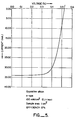
- the current voltage characteristic (50 mV/second) of the cell in response to light intensity of 70 mW/cm 2 from a calibrated solar simulator ELH-type tungsten halogen source is. shown in Figure 4. Efficiency of 10.1% was observed for the matte surfaced cells and 7.8% for the polished surface cells.
- an analogous 2- electrode cell was constructed as set forth below in Example 2.
- Example 2 A 2-electrode LIS Junction Cell With Single Crystal Silicon Semiconductor.
- a thin cell was constructed in the following manner:
- the working electrode was fashioned from an n-type polished single crystal wafer with crystalline orientation (100) and resistivity 4-9 ohm-cm.
- First the same was oxidized in wet oxygen at 1100 °C to form a dense oxide on both sides of ° approximately 8000 A in thickness.
- the perimeter of the sample was coated with positive photoresist to define an uncoated square area slightly larger than one square centimeter. After baking at 90°C for 30 minutes (to harden the photoresist), the sample was etched for 12 minutes in semiconductor grade buffered oxide etch to remove the oxide in the defined square.
- Example 2 the sample was treated in Transene solar cell etchant type 200 in the manner described in Example 1 to provide the defined area with a matte finish.
- An ohmic contact to the backside was made as described in Example 1, and immediately prior to use, the sample was etched in 1:10 HF:H 2 0 and rinsed in methanol.
- the counter electrode was fashioned with indium tin oxide (ITO) coated glass obtained from OCLI having a sheet resistivity of approximately 10 ohms per square and an integrated transmission of 85-90%.
- ITO indium tin oxide
- two .5 mm holes were drilled in the ITO coated glass with an ultrasonic impact grinder made by Raytheon Corporation.
- four .25 square centimeter stainless steel masks were placed on the sample such that they defined a total area slightly larger than 1 square centimeter and equal to the area previously defined on the 0 silicon electrode.
- a 150 A layer of Ti (for its adhesion 0 properties) followed by a 1000 A layer of Au (for its conductive properties) were then evaporated in a filament evaporator at a pressure of 5 x 10 -6 torr.
- the removal of the masks left four .25 square centimeter transparent areas separated by two crossed grid lines of approximately 1 mm in width.
- the working and counter electrodes were then clamped together and glued with 5 minute epoxy.
- Two syringe needles were epoxied into the holes in the ITO coated glass to provide a means for introducing the solution.
- the contents of the solution were identical to whose used in Example 1, however, the concentrations were modified to suit the two electrode configuration using the conditions as set forth above.
- the solvent was methanol with 1.5M lithium perchlorate electrolyte, .12M Fc-OH and .16M Fc + -OH .
- a semiconductor photoanode was prepared of the formula n-GaAs. ⁇ .72 P 0.28 obtained as an epilayer deposited on n +- GaAs or n -GaP substrate by vapor phase epitaxial techniques. The layer thickness was large enough (0.1 mm) such that no photoelectrochemical effects would be ascribable to the substrate material. Samples (0.1 cm 2 ) were mounted as photoelectrodes by forming ohmic contacts to the substrates by evaporation of In at 1 X 10 -6 torr and annealing them under nitrogen at 400°C for 15 minutes. Samples were attached to a copper wire with silver paint and insulated with epoxy cement. Light sources utilized were either sunlight or a calibrated W-halogen ELH lamp with a ground glass diffuser. The samples were etched with 1:1 HF:H 2 O 2 for 15 seconds, rinsed with H 2 0 and air dried before use.
- Example 4 A 3-electrode Cell With n-GaAs Semiconductor
- Photoelectrochemical cells were prepared utilizing n-GaAs semiconductor electrodes in 0.1 M ferrocene (Fc),0.5 mM ferrocenium (Fc ) in acetonitrile and 1.0 M [(C 2 H 5 ) 4 N] + [BF 4 - ].
- Example 5 A 3-electrode Cell With Single Crystal p-type Silicon
- Electrodes were fashioned from 4-9 ohm-cm boron doped (100) oriented single crystal silicon obtained from Siltec. The preparation was identical to that described in Example 1 0 except that ohmic contact was made by evaporating 2000 A of aluminum and sintering at 650 degrees centigrade for 15 minutes. A solution of .15 M bis(cyclopentadienyl)cobalt perchlorate and .5mM bis(cyclopentadienyl)cobalt was dissolved in acetonitrile with 1M tetraethylammonium boron terafluoride as electrolyte. The redox potential of the solution was -0.78 volts vs. SCE, as measured through a Luggin capillary vs. a platinum foil electrode.
- Example 1 A sample, mounted as described in Example 1 and measured to be .143 square centimeters in area, was etched in 48% HF for 15 seconds, rinsed with water, then with acetonitrile, air dried and inserted into a three electrode cell fitted with a Luggin capillary as described in Example 1. Under 88 mW/cm2 of ELH illumination, we observe an open circuit voltage of .49 V, a short circuit current of 26 mA/cm2 and a conversion efficiency of 6%. It is predicted that this result will be improved with the addition of a matte etch to the surface treatment and further improved in a two electrode configuration similar to that described in Example 2.
- Example 6 A 3-electrode LIS Cell With Amorphous Silicon Semiconductor.
- a layer of amorphous silicon was deposited by rf plasma de- composition on a stainless steel substrate.
- a 100 A layer of phosphorous doped amorphous silicon followed by a .5 micron layer of intrinsic amorphous silicon characterized the deposition.
- the backside was contacted with a copper wire threaded through a glass rod.
- An electrical connection to the backside was made with silver epoxy and then the electrode was attached to the rod with insulating epoxy.
- the backside and the perimeter of the front side were also covered with insulating and opaque epoxy to define the electrode area. The area was measured to be .28 square centimeters.
- the solution used in this cell had the same ingredients as described in Example 1.
- the solution was methanol with 1M lithium perchlorate and the redox pair was .15 M Fc-OH, .5 mM Fc -OH.
- a Luggin capillary was used to minimize uncompensated resistance.
- the low current values were attributed to solution absorption.
- Example 7 A 2-electrode LIS Cell With Amorphous Silicon Semiconductor.
- a thin layer of amorphous silicon was deposited by rf plasma decomposition on a degenerately doped n-type single 0 crystal silicon substrate.
- a 1000 A layer of n+ amorphous silicon followed by a 0.5 micron layer of intrinsic amorphous silicon characterized the deposition.
- An ohmic back contact was accomplished as in Examples 1 and 2 with Ga-In eutectic.
- the counter electrode was fashioned with ITO coated glass supplied by OCLI having the characteristics described in Example 2. As in Example 2, first two holes were ultrasonically drilled in the ITO coated glass. Then the glass was masked with a square silicon slice of area .065 square centimeters.
- the masked glass was placed in a filament evaporator and, at a system pressure of 5 X 10 -6 torr, 0 5000 A of aluminum was evaporated onto it.
- a larger square silicon mask of area .15 square centimeters was then placed on the ITO coated glass and the region surrounding the mask 0 was coated with an 8000 A insulating film of chemical-vapor- deposited Si0 2 .
- the counter electrode and the working electrode were then clamped together and epoxied (as in Example 2).
- the solution identical to the one in Example 2, was introduced by means of syringes which were epoxied to the previously drilled holes.
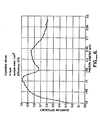
- a conversion efficiency of 3.1% was observed under 100 mw/cm 2 of ELH-type irradiation. As shown in Figure 7, there was observed an increase in efficiency after the cell was held at maximum power for approximately 1.5 hours. Open circuit voltage increased from .77 volts to .85 volts while short circuit current increased from 6.9 mA/cm 2 to 7.2 mA/cm 2 . The corresponding increase in efficiency was from 3.1% to 3.5%. The increase in efficiency was attributed to the formation of an optimized thickness of oxide on the working electrode surface which creates the optimized LIS structure discussed in this application. It was noted that the characteristics of the amorphous silicon used were less than optimal. It is expected that a reflecting substrate and an optimized thickness will yield a dramatic improvement in conversion efficiency.
- Example 8 A 2-electrode Cell With n-type Polycrystalline Silicon Semiconductor.
- Samples of n-type polycrystalline silicon were obtained from Wacker Siltronic. The samples were characterized by a resistivity of 1-3 ohm-cm and a preferred crystal orientation of (100). They were diced into one square centimeter squares with a diamond saw, then treated for 1.5 hours in the Transene matte etch under the conditions described in Example 1. Following the matte etch a sample was further etched in 10:1 H 2 O:HF for 10 minutes and rinsed in H 2 O. A square mask of approximate area .36 square centimeters was then placed in the center of the sample and the sample was : covered with a 7000 A insulating layer of chemical-vapor- deposited Si0 2 . Upon removal of the mask, a working electrode with a bare silicon area surrounded by an insulating oxide was obtained. Ohmic contact to the backside was made with gallium indium eutectic as in Example 2.
- the counter electrode was fashioned with ITO coated glass in the general manner described in Example 2; however, only one masking square was used, and the resulting cell area was therefore .25 square centimeters.
- Example 2 After a 30 second etch in 10:1 H 2 O:HF followed by a methanol rinse the working electrode was clamped to the counter electrode and epoxied. As in Example 2, syringe needles were epoxied to holes in the ITO coated glass, and the solution was introduced. The solution was identical to the one described in Example 2.
Landscapes
- Engineering & Computer Science (AREA)
- Power Engineering (AREA)
- Chemical & Material Sciences (AREA)
- Chemical Kinetics & Catalysis (AREA)
- Electrochemistry (AREA)
- General Chemical & Material Sciences (AREA)
- Microelectronics & Electronic Packaging (AREA)
- Photovoltaic Devices (AREA)
- Hybrid Cells (AREA)
Applications Claiming Priority (2)
| Application Number | Priority Date | Filing Date | Title |
|---|---|---|---|
| US451336 | 1982-12-20 | ||
| US06/451,336 US4459343A (en) | 1982-12-20 | 1982-12-20 | Nonaqueous electrolyte photoelectrochemical cell |
Publications (1)
| Publication Number | Publication Date |
|---|---|
| EP0114493A1 true EP0114493A1 (fr) | 1984-08-01 |
Family
ID=23791813
Family Applications (1)
| Application Number | Title | Priority Date | Filing Date |
|---|---|---|---|
| EP83307731A Withdrawn EP0114493A1 (fr) | 1982-12-20 | 1983-12-20 | Cellule photo-électrochimique |
Country Status (5)
| Country | Link |
|---|---|
| US (1) | US4459343A (fr) |
| EP (1) | EP0114493A1 (fr) |
| JP (1) | JPS59167975A (fr) |
| CA (1) | CA1192293A (fr) |
| IL (1) | IL70453A0 (fr) |
Families Citing this family (5)
| Publication number | Priority date | Publication date | Assignee | Title |
|---|---|---|---|---|
| US4764439A (en) * | 1982-12-20 | 1988-08-16 | Sera Solar Corporation | Photoelectrochemical cell |
| EP0319182B1 (fr) * | 1987-11-30 | 1993-09-29 | EIC Laboratories, Inc. | Protection contre une surcharge de batteries secondaires non aqueuses |
| US4857423A (en) * | 1987-11-30 | 1989-08-15 | Eic Labotatories, Inc. | Overcharge protection of secondary, non-aqueous batteries |
| US5348627A (en) * | 1993-05-12 | 1994-09-20 | Georgia Tech Reserach Corporation | Process and system for the photoelectrochemical etching of silicon in an anhydrous environment |
| JP3713900B2 (ja) * | 1996-07-19 | 2005-11-09 | ソニー株式会社 | 負極材料及びこれを用いた非水電解液二次電池 |
-
1982
- 1982-12-20 US US06/451,336 patent/US4459343A/en not_active Expired - Fee Related
-
1983
- 1983-12-15 IL IL70453A patent/IL70453A0/xx unknown
- 1983-12-19 CA CA000443599A patent/CA1192293A/fr not_active Expired
- 1983-12-20 JP JP58240802A patent/JPS59167975A/ja active Pending
- 1983-12-20 EP EP83307731A patent/EP0114493A1/fr not_active Withdrawn
Non-Patent Citations (7)
| Title |
|---|
| APPLIED PHYSICS LETTERS, vol. 38, no. 9, May 1981 New York, USA S. MENEZES et al. "Electrolyte-oxide-semiconductor junction at the p/-InP/V2+-V3+interface" pages 710-712 * |
| EXTENDED ABSTRACTS, vol. 80-2, October 1980, Princeton, USA H.J. BYKER et al. "Photoelectrochemical corrosion of n-type silicon in nonaqueous electrolytes" abstract no. 292, pages 750, 751 * * |
| JOURNAL OF THE ELCTROCHEMICAL SOCIETY, vol. 128, no. 8, August 1981, Manchester, USA P. SINGH et al. "Mechanisms of charge transfer at the n-GaAs/room temperature molten salt electrolyte interface", pages 1724-1731 * |
| JOURNAL OF THE ELECTROCHEMICAL SOCIETY, vol. 128, no. 11, November 1981, Manchester, USA R. NOUFI et al. "Photoelectrochemical evaluation of the n-CdSe/methanol/ferro-ferricyanide system", pages 2363-2366 * |
| JOURNAL OF THE ELECTROCHEMICAL SOCIETY, vol. 128, no. 6, June 1981, Princeton, USA Y. NAKATO et al. "Surface intermediates of an n-type gallium phosphide electrode as related with the shifts of the surface band energy induced by oxidants in solution", pages 1300-1304 * |
| JOURNAL OF THE ELECTROCHEMICAL SOCIETY, vol. 129, no. 8, August 1982, Manchester, USA M.E. LANGMUIR et al. "Electrochemical photovoltaic cells based on n-GaAs and the triiodide/lodide redox couple in acetonitrile", pages 1705-1710 * |
| JOURNAL OF THE ELECTROCHEMICAL SOCIETY, vol. 129, no. 9, September 1982, Manchester, USA R.E. MALPAS "The electrochemistry and photoelectrochemistry of an aqueous ferrocene/ferricenium redox couple at platinum, N-silicon and N-indium phosphide electrodes" * |
Also Published As
| Publication number | Publication date |
|---|---|
| CA1192293A (fr) | 1985-08-20 |
| US4459343A (en) | 1984-07-10 |
| JPS59167975A (ja) | 1984-09-21 |
| IL70453A0 (en) | 1984-03-30 |
Similar Documents
| Publication | Publication Date | Title |
|---|---|---|
| Aharon‐Shalom et al. | Efficient p‐InP (Rh‐H alloy) and p‐InP (Re‐H alloy) hydrogen evolving photocathodes | |
| Heller et al. | Spectral response and efficiency relations in semiconductor liquid junction solar cells | |
| EP0002109B1 (fr) | Procédé pour la fabrication des couches minces et photoconductives et des cellules solaires en employant lesdites couches minces et photoconductives | |
| US4436558A (en) | Electrochemical photovoltaic cell having ternary alloy film | |
| Bockris et al. | The Rate of the Photoelectrochemical Generation of Hydrogen at p‐Type Semiconductors | |
| Bard et al. | The concept of Fermi level pinning at semiconductor/liquid junctions. Consequences for energy conversion efficiency and selection of useful solution redox couples in solar devices | |
| US4225408A (en) | Process for electrolytically preparing a semiconducting film on a flexible substrate | |
| Hodes et al. | Heterojunction silicon/indium tin oxide photoelectrodes: development of stable systems in aqueous electrolytes and their applicability to solar energy conversion and storage | |
| US4656103A (en) | Liquid junction photoelectrodes using amorphous silicon-based thin film semiconductor | |
| US4613417A (en) | Semiconductor etching process | |
| Anderson et al. | Becquerel effect solar cell | |
| US4492811A (en) | Heterojunction photovoltaic device | |
| Takahashi et al. | Resistivity, carrier concentration, and carrier mobility of electrochemically deposited CdTe films | |
| US4084044A (en) | Liquid-semiconductor photocell using sintered electrode | |
| US4459343A (en) | Nonaqueous electrolyte photoelectrochemical cell | |
| Nakato et al. | Photovoltage and stability of an n-type silicon semiconductor coated with metal or metal-free phthalocyanine thin films in aqueous redox solutions | |
| US3271198A (en) | Electrolytic semiconductor photocell | |
| US4764439A (en) | Photoelectrochemical cell | |
| Neumann‐Spallart et al. | Photoelectrochemical properties of semiconducting cadmium mercury telluride thin films with bandgaps between 1.47 and 1.08 eV | |
| Thompson et al. | Photoelectrochemical Generation of Chlorine on Catalytically Modified n‐Silicon/Indium Tin Oxide Anodes | |
| Nakato et al. | pn Junction silicon electrode coated with noble metal for efficient solar photoelectrolysis of hydrogen iodide. | |
| Chartier et al. | Photoassisted interfacial charge transfers at inhomogeneous semiconducting film-electrolyte junction in photoelectrochemical cells: Case of CdS and CdS (Al) sprayed films on to conductive glass | |
| US4628013A (en) | Photoelectrochemical cell | |
| CA1138080A (fr) | Cellule photoelectrique a semiconducteur a jonction liquide utilisant une electrode en gaas a surface modifiee | |
| US4608750A (en) | Preparation of photovoltaic device by electrochemical deposition |
Legal Events
| Date | Code | Title | Description |
|---|---|---|---|
| PUAI | Public reference made under article 153(3) epc to a published international application that has entered the european phase |
Free format text: ORIGINAL CODE: 0009012 |
|
| AK | Designated contracting states |
Designated state(s): DE FR GB IT |
|
| 17P | Request for examination filed |
Effective date: 19841206 |
|
| 17Q | First examination report despatched |
Effective date: 19860505 |
|
| STAA | Information on the status of an ep patent application or granted ep patent |
Free format text: STATUS: THE APPLICATION IS DEEMED TO BE WITHDRAWN |
|
| 18D | Application deemed to be withdrawn |
Effective date: 19861117 |
|
| RIN1 | Information on inventor provided before grant (corrected) |
Inventor name: GRONET, CHRISTIAN MATTHEW Inventor name: COGAN, GEORGE WILLIAM Inventor name: GIBBONS, JAMES FRANKLIN Inventor name: LEWIS, NATHAN SAUL |