EP0114736A1 - Méthode pour doper, d'une façon contrôlée et uniforme, du silicium obtenu par fusion par zone - Google Patents
Méthode pour doper, d'une façon contrôlée et uniforme, du silicium obtenu par fusion par zone Download PDFInfo
- Publication number
- EP0114736A1 EP0114736A1 EP19840300221 EP84300221A EP0114736A1 EP 0114736 A1 EP0114736 A1 EP 0114736A1 EP 19840300221 EP19840300221 EP 19840300221 EP 84300221 A EP84300221 A EP 84300221A EP 0114736 A1 EP0114736 A1 EP 0114736A1
- Authority
- EP
- European Patent Office
- Prior art keywords
- silicon
- rod
- polycrystalline silicon
- oxygen
- accordance
- Prior art date
- Legal status (The legal status is an assumption and is not a legal conclusion. Google has not performed a legal analysis and makes no representation as to the accuracy of the status listed.)
- Granted
Links
- 0 CC(C)CC*1CCCC1 Chemical compound CC(C)CC*1CCCC1 0.000 description 2
Images

Classifications
-
- C—CHEMISTRY; METALLURGY
- C30—CRYSTAL GROWTH
- C30B—SINGLE-CRYSTAL GROWTH; UNIDIRECTIONAL SOLIDIFICATION OF EUTECTIC MATERIAL OR UNIDIRECTIONAL DEMIXING OF EUTECTOID MATERIAL; REFINING BY ZONE-MELTING OF MATERIAL; PRODUCTION OF A HOMOGENEOUS POLYCRYSTALLINE MATERIAL WITH DEFINED STRUCTURE; SINGLE CRYSTALS OR HOMOGENEOUS POLYCRYSTALLINE MATERIAL WITH DEFINED STRUCTURE; AFTER-TREATMENT OF SINGLE CRYSTALS OR A HOMOGENEOUS POLYCRYSTALLINE MATERIAL WITH DEFINED STRUCTURE; APPARATUS THEREFOR
- C30B13/00—Single-crystal growth by zone-melting; Refining by zone-melting
- C30B13/08—Single-crystal growth by zone-melting; Refining by zone-melting adding crystallising materials or reactants forming it in situ to the molten zone
- C30B13/10—Single-crystal growth by zone-melting; Refining by zone-melting adding crystallising materials or reactants forming it in situ to the molten zone with addition of doping materials
Definitions
- the present invention relates generally to the making of silicon crystal rods from which silicon wafers are sectioned for use in the fabrication of semiconductor integrated circuits, and more particularly to a method of producing a single crystal rod of silicon with a controlled content of a desired impurity distributed substantially uniformly throughout the silicon single crystal rod.
- the crucible 10 may be made of a material such as fused silica (or quartz).
- a very pure seed crystal 11 is dipped into the molten silicon 12 contained in the crucible 10 and thereafter pulled from the molten silicon 12 at a controlled rate as denoted by the arrows 14, while the melt is cooled at a controlled rate.
- a crystalline rod 16 of solid silicon As the crystal 11 moves upward it brings along with it (i.e. grows) a crystalline rod 16 of solid silicon.
- the end 18 of the rod 16 closest to the pure crystal 11 is referred to as the seed end.
- the other end 20 closest to the silicon melt 12 is referred to as the tang end.
- the middle section 22 of the rod 16 is referred to as the middle.
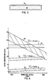
- the curves A, B, C are representative of typical oxygen distribution across the diameter of the crystal rod at the seed, middle, and tang ends of-the -rod 16, respectively.
- the oxygen distribution may range from 30 to 50 parts per million and at the tang end the range is reduced to from 10 to 20 parts per million.
- the oxygen doped silicon produced by the Czochralski process yielded certain characteristics particularly advantageous for use in semicondutor integrated circuit fabrication. More specifically, the oxygen present in the grown silicon rod is beneficial in avoiding warpage of a silicon wafer sectioned therefrom during the multiple heat-cycles of the integrated circuit fabrication process, and in providing an "intrinsic" gettering mechanism for lifetime killing of metallic impurities which may be present in such silicon wafers, as a result of contamination during growth or are introduced during subsequent integrated circuit processing steps.
- Intrinsic gettering is a thermal processing step in which a silicon wafer taken from the crystal rod 16 is exposed to a high temperature anneal in an inert atmosphere during the integrated circuit fabrication process.
- A' cross-sectional view of a typical silicon wafer is shown in Figure 3.
- a region 34 called a denuded zone, relatively free of crystalline defects, forms near the surface of the wafer while crystalline imperfections associated with the silicon oxide precipitates form in the bulk region 36 of the silicon substrate or wafer. These crystalline imperfections act as self-gettering sites and are believed to be an important factor in maintaining high carrier lifetimes throughout a large scale integrated circuit fabrication process.
- the oxygen doped silicon yielded by the Czochralski process also has its disadvantages especially in its application to current very large scale integrated (VLSI) circuit fabrication.
- the silicon produced is not very pure usually containing on the order of 10 14 -10 15 cm -3 boron and 10 16 -10 17 cm 3 carbon impurities.
- the Czochralski silcon growth method neither provides for uniform oxygen distribution nor permits easy control of oxygen content of the silicon grown boules (see Figure 2, for example).
- the nonuniform oxygen concentrations in the grown silicon boules may give rise to relatively large numbers of microdefects in the denuded zone of the silicon wafers sliced therefrom.
- Such high densities of deleterious defects in this active device region are not compatible with large scale, high speed integrated circuits which generally require nearly defect-free silicon surfaces in which uniform oxygen contents not greater than 10 to 20 parts per million may be required.
- float zone process Another well known technique for preparing large diameter _silicon crystals is the float zone process which is capable of producing very pure, low defect density silicon.
- the resulting silicon is used primarily for semiconductor devices requiring excellent bulk properties and high minority carrier lifetimes, such as power devices, for example.
- a polycrystalline silicon rod is passed through a heating zone which melts the portion of the silicon rod being heated which upon cooling becomes of.a single crystalline structure.
- the resulting single crystal silicon boule contains substantially no oxygen (typically 0.1 ppma) and therefore, is not used for integrated circuit fabrication since the wafers taken therefrom exhibit a high degree of warpage after multiple fabrication heat-cycles and in addition, exhibit no intrinsic gettering mechanism due to the lack of oxygen therein.
- oxygen doping of high purity float zone polycrystalline silicon has been tried in the past by, for example, float zoning in an oxygen ambient, but these attempts have been unsuccessful due to melt instabilities associated with the formation of an oxide "scum" on the molten silicon heating zone surface, which results in a lack of single crystalline growth.
- the Czochralski process provides the unintentional oxygen doping of the silicon crystals which allow for their use in integrated circuit fabrication due to the aforementioned advantages of the oxygen doping therein.
- the inability to control the absolute amounts and the uniformity of the oxygen concentrations throughout the silicon crystal grown by the Czochralski process results in various disadvantages.
- the float zone process for producing silicon crystals provides essentially no oxygen thus reducing the application thereof in the semiconductor area to only devices which require certain bulk property characteristics.
- the invention resides broadly in a method of producing a single crystal rod of silicon with a controlled content of a desired impurity distributed substantially uniformly throughout said silicon crystal rod, said method including the steps of: diffusing a polyatomic gaseous element as a desired impurity into the bulk of a polycrystalline rod of silicon, characterized by converting said diffused polycrystalline silicon rod into a single crystal rod of silicon by a float-zoning process.
- the step of diffusing includes the steps of doping the polycrystalline silicon rod with the desired impurity by diffusing the atoms of the polyatomic gaseous element along the grain-boundary surfaces of the small crystallites in a spatially heterogeneous fashion within the polycrystalline silicon rod; and controlling the concentration of the desired impurity dopant in the polycrystalline silicon rod by performing the diffusion of the gaseous element for a predetermined time at a predetermined temperature.
- the polycrystalline silicon rod is placed into a diffusion furnace set at a predetermined temperature; and thereafter, a controlled flow of the polyatomic gaseous element is established across the polycrystalline silicon rod for a predetermined time duration.
- the polycrystalline silicon rod may be diffused in a substantially wet or dry oxygen environment.
- the polycrystalline silicon rod may be diffused in a substantially nitrogen environment.
- the step of converting may be performed in either a substantially inert gas or vacuum environment..
- the method of producing a single crystal rod of silicon with a controlled content of a desired impurity distributed substantially uniformly throughout the silicon crystal rod is exhibited in the illustrations of Figures 4 and 5 which relate to a two-step process including the controlled diffusion of a polyatomic gaseous element like oxygen or nitrogen, for example, into a polycrystalline silicon rod ( Figure 4) and, the subsequent conversion of the diffused rod into a single crystal of silicon by a float-zone method of crystal growth ( Figure 5).
- the present method results in a reproducible technique for the fabrication of silicon crystals containing a controlled amount of the desired impurity which is distributed substantially uniformly throughout the crystal. For example if oxygen is desired, the process may be controlled to diffuse up to 20 parts per million of oxygen substantially uniformly throughout the crystal.
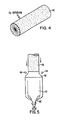
- a polycrystalline rod 40 is diffused in a controlled environment of a polyatomic gaseous element, like oxygen, for example.
- a polyatomic gaseous element like oxygen, for example.
- the oxygen doping concentration is governed by the phenomenon of enhanced diffusion of oxygen atoms along the grain-boundary surfaces of the small crystallites in the rod 40.
- This process may be carried out by placing the polycrystalline silicon rod 40 in a diffusion furnace at a temperature preferably set at 1200 to 1300°C in which a flow of dry or wet oxygen is established. This thermal diffusion process distributes the oxygen in a spatially hetrogeneous fashion throughout the bulk of the silicon rod 40.
- a polycrystalline rod on the order of 1 to 2 inches in diameter was diffused in a diffusion furnace with a flow of dry oxygen at approximately 600 cm 3 per minute at a temperature along the order of 1200°C for a time duration of 336 hours. It is understood however that the magnitude of the oxygen content in the polycrystalline silicon rod is determined by the environmental temperature and duration of time at which the diffusion is carried out.
- the polycrystalline silicon rod 40 which contains a level of oxygen as determined by the diffusion time and temperature of the first step, described hereabove, may be placed in a conventional float-zoning apparatus in an inert gas or vacuum ambient and converted by the float-zoning procedures thereof into an oxygen doped single crystal of silicon as shown at 42.
- This process is performed by moving the oxygen diffused polycrystalline silicon rod 40 through heating elements 44, such as RF coils, for example, which render a molten silicon zone 46 in the polysilicon rod 40.
- heating elements 44 such as RF coils, for example, which render a molten silicon zone 46 in the polysilicon rod 40.
- the final oxygen concentration of the float-zoned crystal at 42 is dependent primarily on the environmental diffusion parameters as described in connection with process step 1..
- the crux of the inventive process is that in this crucible-free, float-zoning process owing to its near unity segregation coefficient, the oxygen will be distributed substantially uniformly both radially and axially throughout the silicon crystal as opposed to the silicon crystals grown by the conventional Czochralski technique which exhibits spatially nonuniform oxygen distributions.
- the high background purity characteristic of silicon produced by the conventional float-zoning process will be maintained substantially in the oxygen-doped, float-zoned silicon crystal formed since any deleterious heavy metal contamination resulting from the diffusion step 1 is removed during the float-zoning step of the process.
- the graph of Figure 6 exhibits various experimental results in fabricating single silicon crystal boules with controlled, uniform oxygen concentrations.
- Curve portions 50, 52 and 54 depict the axial variations of the oxygen concentration of three oxygen-doped silicon crystals fabricated by the aforementioned float-zone procedure compared to the oxygen distribution of a typical silicon boule grown by the Czochralski method as shown by the curve region 56.
- a 30 millimeter diameter polycrystalline rod (Dow-Corning 111-0749-6) was diffusion annealed under a flow of dry-ultra-high purity oxygen in a 3 inch diameter diffusion furnace for 336 hours at 1200°C.
- the oxygen doped rod was then placed in a Westech (Model 145) float-zone refiner and float-zoned in the ⁇ 111> orientation under an inert ultra high purity argon ambient at a pressure of 1000 Torr using a zoning rate of 2 millimeters/minute to produce a 30 millimeter diameter ⁇ 111> oriented silicon crystal (see j Figure 5).
- the oxygen concentrations in the resulting silicon crystal were determined by Fourier-transform infrared spectrometry using Digilab (FTS-14) IR spectrometer.
- the oxygen level at the crystal seed end was about 1 x 10 17 cm -3 (2 ppma) and 2 x 10 17 cm -3 (4 ppma) at the tail end.
- the curve region 50 corresponds to a 25 millimeter diameter polycrystalline silicon rod (Topsil). This rod was diffusion annealed under the same conditions as used for curve region 52. After float-zoning in the ⁇ 100> orientation under an inert argon ambient, the polysilicon rod yielded a 30 millimeter diameter silicon crystal having an oxygen concentration of 16 ppma (8 x 10 17 cm -3 ) at the seed end and a concentration of 18 ppma ( 9 x 10 17 cm -3 ) at the tang end.
- the curve 54 corresponds to a polycrystalline silicon rod of similar dimensions as that of the other two rods associated with curves 50 and 52 and was diffusion- annealed under similar conditions.
- the diametric spread of oxygen concentration for this experimental example was centered about a level of approximately 32 ppma with very little axial change from the seed end to the tang end.
- Polycrystalline silicon rods having varying amounts of residual carbon content were investigated during the experimental process involving the above- described two-step method.
- the specific carbon content of the silicon rods ranged from ⁇ .26 ppma to approximately 1.5 ppma. While the diffused oxygen content in the silicon rods was observed to vary with a changing residual carbon content, the effect of the carbon content on oxygen incorporation in the silicon crystal was inconclusive.
- the preferred method disclosed hereabove is intended for fabricating impurity doped float-zoned silicon boules which exhibit uniform concentrations of the desired impurity.
- This method when applied to polycrystalline silicon rods, results in the production of high-purity float-zone silicon crystals with substantially uniform oxygen concentrations of up to 32 ppma which are not currently attainable utilizing the conventional Czochralski silicon boule fabrication methods of the semiconductor industry.
- the controlled doped silicon material resulting from the preferred process is of special interest in view of its potential as a high quality silicon substrate wafer material for very large scale, high speed integrated circuit applications.
Landscapes
- Chemical & Material Sciences (AREA)
- Engineering & Computer Science (AREA)
- Crystallography & Structural Chemistry (AREA)
- Materials Engineering (AREA)
- Metallurgy (AREA)
- Organic Chemistry (AREA)
- Crystals, And After-Treatments Of Crystals (AREA)
Applications Claiming Priority (2)
| Application Number | Priority Date | Filing Date | Title |
|---|---|---|---|
| US45822283A | 1983-01-14 | 1983-01-14 | |
| US458222 | 1983-01-14 |
Publications (2)
| Publication Number | Publication Date |
|---|---|
| EP0114736A1 true EP0114736A1 (fr) | 1984-08-01 |
| EP0114736B1 EP0114736B1 (fr) | 1986-10-22 |
Family
ID=23819871
Family Applications (1)
| Application Number | Title | Priority Date | Filing Date |
|---|---|---|---|
| EP19840300221 Expired EP0114736B1 (fr) | 1983-01-14 | 1984-01-13 | Méthode pour doper, d'une façon contrôlée et uniforme, du silicium obtenu par fusion par zone |
Country Status (5)
| Country | Link |
|---|---|
| EP (1) | EP0114736B1 (fr) |
| JP (1) | JPS59137393A (fr) |
| CA (1) | CA1237641A (fr) |
| DE (1) | DE3461033D1 (fr) |
| IE (1) | IE56157B1 (fr) |
Cited By (2)
| Publication number | Priority date | Publication date | Assignee | Title |
|---|---|---|---|---|
| CN103160912A (zh) * | 2011-12-08 | 2013-06-19 | 有研半导体材料股份有限公司 | 一种掺杂区熔单晶的制备工艺 |
| WO2014093087A1 (fr) * | 2012-12-11 | 2014-06-19 | Hemlock Semiconductor Corporation | Procédés de formation et d'analyse de silicium dopé |
Families Citing this family (1)
| Publication number | Priority date | Publication date | Assignee | Title |
|---|---|---|---|---|
| JP2000082679A (ja) | 1998-07-08 | 2000-03-21 | Canon Inc | 半導体基板とその作製方法 |
Citations (2)
| Publication number | Priority date | Publication date | Assignee | Title |
|---|---|---|---|---|
| FR1236935A (fr) * | 1958-10-04 | 1960-07-22 | Philips Nv | Procédé de préparation d'une matière, dans lequel au moins une impureté significative est répartie dans une matière fondamentale |
| DE2415717A1 (de) * | 1974-04-01 | 1975-10-16 | Siemens Ag | Verfahren zum gezielten einbringen von dotierungsmaterial in einen halbleiterkristallstab |
-
1983
- 1983-12-14 IE IE294383A patent/IE56157B1/en unknown
- 1983-12-19 CA CA000443597A patent/CA1237641A/fr not_active Expired
-
1984
- 1984-01-11 JP JP423184A patent/JPS59137393A/ja active Pending
- 1984-01-13 EP EP19840300221 patent/EP0114736B1/fr not_active Expired
- 1984-01-13 DE DE8484300221T patent/DE3461033D1/de not_active Expired
Patent Citations (2)
| Publication number | Priority date | Publication date | Assignee | Title |
|---|---|---|---|---|
| FR1236935A (fr) * | 1958-10-04 | 1960-07-22 | Philips Nv | Procédé de préparation d'une matière, dans lequel au moins une impureté significative est répartie dans une matière fondamentale |
| DE2415717A1 (de) * | 1974-04-01 | 1975-10-16 | Siemens Ag | Verfahren zum gezielten einbringen von dotierungsmaterial in einen halbleiterkristallstab |
Cited By (3)
| Publication number | Priority date | Publication date | Assignee | Title |
|---|---|---|---|---|
| CN103160912A (zh) * | 2011-12-08 | 2013-06-19 | 有研半导体材料股份有限公司 | 一种掺杂区熔单晶的制备工艺 |
| CN103160912B (zh) * | 2011-12-08 | 2015-11-11 | 有研半导体材料有限公司 | 一种掺杂区熔单晶的制备工艺 |
| WO2014093087A1 (fr) * | 2012-12-11 | 2014-06-19 | Hemlock Semiconductor Corporation | Procédés de formation et d'analyse de silicium dopé |
Also Published As
| Publication number | Publication date |
|---|---|
| DE3461033D1 (en) | 1986-11-27 |
| JPS59137393A (ja) | 1984-08-07 |
| IE832943L (en) | 1984-07-14 |
| CA1237641A (fr) | 1988-06-07 |
| IE56157B1 (en) | 1991-05-08 |
| EP0114736B1 (fr) | 1986-10-22 |
Similar Documents
| Publication | Publication Date | Title |
|---|---|---|
| CN101187058B (zh) | 硅半导体晶片及其制造方法 | |
| US4040895A (en) | Control of oxygen in silicon crystals | |
| EP1926134B1 (fr) | Procédé de fabrication de tranches de silicium épitaxiale | |
| US4010064A (en) | Controlling the oxygen content of Czochralski process of silicon crystals by sandblasting silica vessel | |
| US6821344B2 (en) | Czochralski pullers including heat shield housings having sloping top and bottom | |
| US7326658B2 (en) | Method for preparing nitrogen-doped annealed wafer and nitrogen-doped and annealed wafer | |
| EP1498517B1 (fr) | Procédé de production de silicium monocristallin, silicium monocristallin et plaquette de silicium | |
| US4436577A (en) | Method of regulating concentration and distribution of oxygen in Czochralski grown silicon | |
| KR100720366B1 (ko) | 에피텍셜 웨이퍼 기판에 사용되는 증가형 n-타입 실리콘물질 및 이의 제조방법 | |
| US6365461B1 (en) | Method of manufacturing epitaxial wafer | |
| EP0206541B1 (fr) | Monocristaux d'arséniure de gallium et procédé pour sa fabrication | |
| KR20100061360A (ko) | 실리콘 단결정 및 그 육성방법, 실리콘 웨이퍼 및 그 제조방법 | |
| US6802899B1 (en) | Silicon single crystal wafer and manufacturing process therefor | |
| KR19990045179A (ko) | 실리콘 기판 및 그 제조 방법 | |
| US6056931A (en) | Silicon wafer for hydrogen heat treatment and method for manufacturing the same | |
| US5392729A (en) | Method of producing silicon single crystal | |
| EP0114736B1 (fr) | Méthode pour doper, d'une façon contrôlée et uniforme, du silicium obtenu par fusion par zone | |
| KR20030019472A (ko) | 디누디드 존을 갖는 에피택셜 실리콘 웨이퍼를 형성하는방법 및 장치 | |
| US4545849A (en) | Method for control of oxygen in silicon crystals | |
| EP1746186B1 (fr) | Procede de fabrication d'un monocristal de silicium | |
| US6669777B2 (en) | Method of producing a high resistivity silicon wafer utilizing heat treatment that occurs during device fabrication | |
| JP4080657B2 (ja) | シリコン単結晶インゴットの製造方法 | |
| CN100430531C (zh) | 丘克拉斯基提拉器 | |
| JP4463950B2 (ja) | シリコンウエーハの製造方法 | |
| JPH08290995A (ja) | シリコン単結晶及びその製造方法 |
Legal Events
| Date | Code | Title | Description |
|---|---|---|---|
| PUAI | Public reference made under article 153(3) epc to a published international application that has entered the european phase |
Free format text: ORIGINAL CODE: 0009012 |
|
| AK | Designated contracting states |
Designated state(s): BE DE FR GB |
|
| 17P | Request for examination filed |
Effective date: 19850130 |
|
| GRAA | (expected) grant |
Free format text: ORIGINAL CODE: 0009210 |
|
| AK | Designated contracting states |
Kind code of ref document: B1 Designated state(s): BE DE FR GB |
|
| REF | Corresponds to: |
Ref document number: 3461033 Country of ref document: DE Date of ref document: 19861127 |
|
| ET | Fr: translation filed | ||
| PLBE | No opposition filed within time limit |
Free format text: ORIGINAL CODE: 0009261 |
|
| STAA | Information on the status of an ep patent application or granted ep patent |
Free format text: STATUS: NO OPPOSITION FILED WITHIN TIME LIMIT |
|
| 26N | No opposition filed | ||
| BERE | Be: lapsed |
Owner name: WESTINGHOUSE ELECTRIC CORP. Effective date: 19880131 |
|
| PG25 | Lapsed in a contracting state [announced via postgrant information from national office to epo] |
Ref country code: FR Free format text: LAPSE BECAUSE OF NON-PAYMENT OF DUE FEES Effective date: 19880930 |
|
| REG | Reference to a national code |
Ref country code: FR Ref legal event code: ST |
|
| PG25 | Lapsed in a contracting state [announced via postgrant information from national office to epo] |
Ref country code: GB Effective date: 19890113 |
|
| PG25 | Lapsed in a contracting state [announced via postgrant information from national office to epo] |
Ref country code: BE Effective date: 19890131 |
|
| GBPC | Gb: european patent ceased through non-payment of renewal fee | ||
| PG25 | Lapsed in a contracting state [announced via postgrant information from national office to epo] |
Ref country code: DE Effective date: 19891003 |