EP0114765A2 - Verfahren und Vorrichtung für die Ionenanalyse von nichtleitenden Proben - Google Patents
Verfahren und Vorrichtung für die Ionenanalyse von nichtleitenden Proben Download PDFInfo
- Publication number
- EP0114765A2 EP0114765A2 EP84400078A EP84400078A EP0114765A2 EP 0114765 A2 EP0114765 A2 EP 0114765A2 EP 84400078 A EP84400078 A EP 84400078A EP 84400078 A EP84400078 A EP 84400078A EP 0114765 A2 EP0114765 A2 EP 0114765A2
- Authority
- EP
- European Patent Office
- Prior art keywords
- target
- sample
- bombarded
- ions
- electron beam
- Prior art date
- Legal status (The legal status is an assumption and is not a legal conclusion. Google has not performed a legal analysis and makes no representation as to the accuracy of the status listed.)
- Granted
Links
- 238000000034 method Methods 0.000 title claims abstract description 13
- 238000004458 analytical method Methods 0.000 title claims abstract description 12
- 150000002500 ions Chemical class 0.000 claims abstract description 31
- 238000010884 ion-beam technique Methods 0.000 claims abstract description 7
- 238000010894 electron beam technology Methods 0.000 claims description 13
- 230000003287 optical effect Effects 0.000 claims description 12
- 238000000605 extraction Methods 0.000 abstract description 5
- 238000006386 neutralization reaction Methods 0.000 abstract 1
- PNEYBMLMFCGWSK-UHFFFAOYSA-N aluminium oxide Inorganic materials [O-2].[O-2].[O-2].[Al+3].[Al+3] PNEYBMLMFCGWSK-UHFFFAOYSA-N 0.000 description 4
- 239000002244 precipitate Substances 0.000 description 4
- XEEYBQQBJWHFJM-UHFFFAOYSA-N Iron Chemical compound [Fe] XEEYBQQBJWHFJM-UHFFFAOYSA-N 0.000 description 3
- 230000000694 effects Effects 0.000 description 3
- 230000005684 electric field Effects 0.000 description 3
- 238000010849 ion bombardment Methods 0.000 description 3
- VYPSYNLAJGMNEJ-UHFFFAOYSA-N Silicium dioxide Chemical compound O=[Si]=O VYPSYNLAJGMNEJ-UHFFFAOYSA-N 0.000 description 2
- 238000009792 diffusion process Methods 0.000 description 2
- 238000009826 distribution Methods 0.000 description 2
- 230000003993 interaction Effects 0.000 description 2
- 229910052760 oxygen Inorganic materials 0.000 description 2
- 239000001301 oxygen Substances 0.000 description 2
- 230000006978 adaptation Effects 0.000 description 1
- QVGXLLKOCUKJST-UHFFFAOYSA-N atomic oxygen Chemical compound [O] QVGXLLKOCUKJST-UHFFFAOYSA-N 0.000 description 1
- 238000007664 blowing Methods 0.000 description 1
- 210000000988 bone and bone Anatomy 0.000 description 1
- 150000001875 compounds Chemical class 0.000 description 1
- 238000005336 cracking Methods 0.000 description 1
- 230000007423 decrease Effects 0.000 description 1
- 230000001066 destructive effect Effects 0.000 description 1
- 238000010586 diagram Methods 0.000 description 1
- 238000007599 discharging Methods 0.000 description 1
- 239000000428 dust Substances 0.000 description 1
- 230000005686 electrostatic field Effects 0.000 description 1
- 238000001704 evaporation Methods 0.000 description 1
- 230000008020 evaporation Effects 0.000 description 1
- 239000000284 extract Substances 0.000 description 1
- 238000001914 filtration Methods 0.000 description 1
- 230000004907 flux Effects 0.000 description 1
- 238000002513 implantation Methods 0.000 description 1
- 238000010249 in-situ analysis Methods 0.000 description 1
- 229910052500 inorganic mineral Inorganic materials 0.000 description 1
- 239000011810 insulating material Substances 0.000 description 1
- 238000001886 ion microscopy Methods 0.000 description 1
- 229910052742 iron Inorganic materials 0.000 description 1
- 230000000155 isotopic effect Effects 0.000 description 1
- 239000011159 matrix material Substances 0.000 description 1
- 239000002184 metal Substances 0.000 description 1
- 229910052751 metal Inorganic materials 0.000 description 1
- 230000005012 migration Effects 0.000 description 1
- 238000013508 migration Methods 0.000 description 1
- 239000011707 mineral Substances 0.000 description 1
- 239000000203 mixture Substances 0.000 description 1
- 230000003472 neutralizing effect Effects 0.000 description 1
- -1 oxygen ions Chemical class 0.000 description 1
- 239000002245 particle Substances 0.000 description 1
- 238000002161 passivation Methods 0.000 description 1
- 238000002360 preparation method Methods 0.000 description 1
- 239000011435 rock Substances 0.000 description 1
- 239000004065 semiconductor Substances 0.000 description 1
- 150000004760 silicates Chemical class 0.000 description 1
- 239000000377 silicon dioxide Substances 0.000 description 1
- 238000004611 spectroscopical analysis Methods 0.000 description 1
- 239000000126 substance Substances 0.000 description 1
- 230000001629 suppression Effects 0.000 description 1
- 210000001519 tissue Anatomy 0.000 description 1
Images

Classifications
-
- H—ELECTRICITY
- H01—ELECTRIC ELEMENTS
- H01J—ELECTRIC DISCHARGE TUBES OR DISCHARGE LAMPS
- H01J37/00—Discharge tubes with provision for introducing objects or material to be exposed to the discharge, e.g. for the purpose of examination or processing thereof
- H01J37/02—Details
- H01J37/026—Means for avoiding or neutralising unwanted electrical charges on tube components
-
- G—PHYSICS
- G01—MEASURING; TESTING
- G01N—INVESTIGATING OR ANALYSING MATERIALS BY DETERMINING THEIR CHEMICAL OR PHYSICAL PROPERTIES
- G01N23/00—Investigating or analysing materials by the use of wave or particle radiation, e.g. X-rays or neutrons, not covered by groups G01N3/00 – G01N17/00, G01N21/00 or G01N22/00
- G01N23/22—Investigating or analysing materials by the use of wave or particle radiation, e.g. X-rays or neutrons, not covered by groups G01N3/00 – G01N17/00, G01N21/00 or G01N22/00 by measuring secondary emission from the material
- G01N23/225—Investigating or analysing materials by the use of wave or particle radiation, e.g. X-rays or neutrons, not covered by groups G01N3/00 – G01N17/00, G01N21/00 or G01N22/00 by measuring secondary emission from the material using electron or ion
Definitions
- the invention relates to a method and a device for ionic analysis of an insulating sample.
- a target is bombarded with a beam of primary ions on the surface of the sample to be analyzed.
- the target then emits negative ions which are collected by a system which gives the distribution map of the elements present on the surface of the sample.
- the electrons produced on the extraction electrode are repelled by the sample and, on the other hand, the electrostatic field extracts at the same time secondary electrons emitted by the target: the emission of secondary electrons is much more intense than the ionic emission, so that, whatever the sign of the primary bombardment ions, there always appears a positive charge on the surface. This emission is further increased when the output work is lowered by Cs +, K + bombardment or a blowing of Cs vapors. In addition, on heterogeneous samples, this charge can vary from one place to another depending on the yield of secondary electrons of the place considered. Experience shows that this positive charge is such that any ion microscopy from negative secondary ions is impossible with traditional methods.
- the object of the invention is to overcome this impossibility and to propose a method allowing the effective suppression of the load effects.
- a major advantage of the invention is therefore to supply the surface of the sample with electrons without these having any harmful interaction with the sample (such as the problems of diffusion of certain elements under electronic bombardment too much energy, or cracking problems).
- a filament brought to substantially the same negative potential as the sample emits said electron beam.
- the electron beam is, after emission, deflected by a magnetic prism to be brought into coincidence with the optical axis of the negative ion beam emitted by the target.
- the electrons leaving the target in the optical axis are used to obtain an electronic image of the sample.
- the invention also provides a device for the ionic analysis of an insulating sample brought to a predetermined negative potential, of the type which comprises a source of primary bombardment ions directed at a target on the surface of the sample to be analyzed, and, in the optical axis of the device, a mass spectrograph.
- said device also comprises a source brought substantially to the potential of the sample emitting an electron beam, and means for directing said beam on said target perpendicular to the bombarded surface.
- said means consist of a magnetic prism, and magnetic compensation is provided for the deviation by said prism of the trajectory of the negative ions emitted by the target.
- the prism is a double magnetic prism, deflecting the electrons which leave the target in the optical axis, and there is provided a second analyzer delivering an electronic image of the sample.
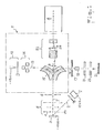
- the secondary negative ion beam emitted by the target is accelerated by the extracting electrode 4, brought to ground, passes through a collecting optic 5 then the diaphragm 6 located on the cross-over.
- a collecting optic 5 On the same optical axis 7 is arranged the mass spectrograph 8 on which the invention does not relate.
- the system 11 for suppressing the effects of load is interposed between the diaphragm 6 and the spectrograph 8.
- This system 11 comprises an electron source 12 located on an axis 13 intersecting the general optical axis 7 at an angle, which, in the figure, is 90 °.
- the electrons come from a filament brought to a potential of - 4,500 V; they are accelerated by an extracting electrode at zero potential, and pass through a conventional centering device 14. They are deflected by a magnetic prism 15 which thus brings them back to the optical axis.
- the electron beam passes through the diaphragm 6, a cross-over common to the ion beam and to the electron beam; then it crosses the emission lens 5 and arrives in the zone between the object 3 and the extraction electrode 4, zone where the electric field prevails which makes it possible to accelerate the negative particles emitted by the surface.
- This electric field then brakes the electrons, their energy gradually decreases and is substantially canceled out at the surface.
- the emission lens 5 acts on the electronic trajectories as it does on those of negative ions. It follows that the electrons arrive at the surface with a lateral component of the velocity which is very low, their normal component at the surface being zero or practically zero (and not creating, in any event, any harmful interaction with the sample). Electrons that are not used to neutralize the surface of the sample turn back, with secondary electrons emitted from the surface of the sample (and of course with negative ions).
- the magnetic prism 15 used to deflect the discharge electrons by 90 ° is advantageously twofold: it deflects the electrons leaving the target in the opposite direction, thus making it possible to observe the electronic image formed from the backscattered electrons. or reflected, or that of the image obtained with the secondary electrons produced either by the primary ion bombardment, or by the impact of the incident electrons.
- a conventional annex analyzer device is provided on the path of the deflected electron beam 16: selection blades 17, electrostatic centering 18, post-accelerating optics 19, projection optics 20, screen 21.
- the presence of the prism 15 on the optical axis 7 also produces a slight angle deviation 9 of the trajectory of the secondary ions.
- An additional magnetic system 22 is therefore provided to compensate for this rotation whatever the mass of the secondary ions.
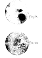
- FIG. 2A shows a global ion image - that is to say without mass filtering of the ions - obtained by ion bombardment of an iron matrix.
- the dark spots correspond to disturbances in the secondary ion emission induced by the presence of small precipitates of alumina (respective dimensions: approximately 10 and 20 / ⁇ m) with very low electrical conductivity.
- FIG. 2B shows an ion image obtained under the same ion bombardment conditions but, this time, with the intervention of a low energy electron beam ((10 eV) according to the invention.
- alumina becomes perceptible, providing information on the real dimensions of these objects and highlighting for each of them the existence of an internal structure.
- FIG. 3A is a global ionic image obtained, as before, by bombardment of an iron-metal target rich in insulating precipitates of alumina.
- this device for discharging insulating samples on a conventional ion analyzer allows the analysis, until now impossible, of negatively charged oxygen ions emitted from insulating materials, as are most of the compounds of the oxygen, oxides and silicates, and makes possible the punctual analysis of the isotopic composition of this element in objects of astrophysical interest: key mineral phases of meteorites, interplanetary dust.
- the method according to the invention which in no way modifies the physical or chemical appearance of the sample analyzed, allows all kinds of in situ analysis, the non-destructive nature of which is essential.
Landscapes
- Chemical & Material Sciences (AREA)
- Analytical Chemistry (AREA)
- Physics & Mathematics (AREA)
- Health & Medical Sciences (AREA)
- Life Sciences & Earth Sciences (AREA)
- Biochemistry (AREA)
- General Health & Medical Sciences (AREA)
- General Physics & Mathematics (AREA)
- Immunology (AREA)
- Pathology (AREA)
- Analysing Materials By The Use Of Radiation (AREA)
Applications Claiming Priority (2)
| Application Number | Priority Date | Filing Date | Title |
|---|---|---|---|
| FR8300538A FR2542089B1 (fr) | 1983-01-14 | 1983-01-14 | Procede et dispositif pour l'analyse ionique d'un echantillon isolant |
| FR8300538 | 1983-01-14 |
Publications (3)
| Publication Number | Publication Date |
|---|---|
| EP0114765A2 true EP0114765A2 (de) | 1984-08-01 |
| EP0114765A3 EP0114765A3 (en) | 1984-08-29 |
| EP0114765B1 EP0114765B1 (de) | 1987-11-19 |
Family
ID=9284946
Family Applications (1)
| Application Number | Title | Priority Date | Filing Date |
|---|---|---|---|
| EP19840400078 Expired EP0114765B1 (de) | 1983-01-14 | 1984-01-13 | Verfahren und Vorrichtung für die Ionenanalyse von nichtleitenden Proben |
Country Status (4)
| Country | Link |
|---|---|
| EP (1) | EP0114765B1 (de) |
| JP (1) | JPS59192946A (de) |
| DE (1) | DE3467624D1 (de) |
| FR (1) | FR2542089B1 (de) |
Cited By (4)
| Publication number | Priority date | Publication date | Assignee | Title |
|---|---|---|---|---|
| US4652753A (en) * | 1983-12-26 | 1987-03-24 | Anelva Corporation | Mass spectrometer capable of analyzing an insulator |
| EP0254128A3 (de) * | 1986-07-25 | 1990-01-03 | Siemens Aktiengesellschaft | Verfahren und Anordnung zur aufladungsfreien Untersuchung einer Probe |
| EP0417354A1 (de) * | 1989-09-15 | 1991-03-20 | Koninklijke Philips Electronics N.V. | Elektronenstrahlgerät mit Ausfladungskompensierung |
| FR2732464A1 (fr) * | 1995-03-30 | 1996-10-04 | Alcatel Cable | Procede et dispositif de verification de la conformite d'un element isolant donne avec un element isolant de reference |
Family Cites Families (2)
| Publication number | Priority date | Publication date | Assignee | Title |
|---|---|---|---|---|
| GB918297A (en) * | 1960-04-07 | 1963-02-13 | William Charles Nixon | Improvements in electron microscopes |
| US3665185A (en) * | 1970-10-19 | 1972-05-23 | Minnesota Mining & Mfg | Ion scattering spectrometer with neutralization |
-
1983
- 1983-01-14 FR FR8300538A patent/FR2542089B1/fr not_active Expired
-
1984
- 1984-01-13 DE DE8484400078T patent/DE3467624D1/de not_active Expired
- 1984-01-13 JP JP59003729A patent/JPS59192946A/ja active Granted
- 1984-01-13 EP EP19840400078 patent/EP0114765B1/de not_active Expired
Cited By (6)
| Publication number | Priority date | Publication date | Assignee | Title |
|---|---|---|---|---|
| US4652753A (en) * | 1983-12-26 | 1987-03-24 | Anelva Corporation | Mass spectrometer capable of analyzing an insulator |
| EP0254128A3 (de) * | 1986-07-25 | 1990-01-03 | Siemens Aktiengesellschaft | Verfahren und Anordnung zur aufladungsfreien Untersuchung einer Probe |
| EP0417354A1 (de) * | 1989-09-15 | 1991-03-20 | Koninklijke Philips Electronics N.V. | Elektronenstrahlgerät mit Ausfladungskompensierung |
| FR2732464A1 (fr) * | 1995-03-30 | 1996-10-04 | Alcatel Cable | Procede et dispositif de verification de la conformite d'un element isolant donne avec un element isolant de reference |
| EP0740148A1 (de) * | 1995-03-30 | 1996-10-30 | Alcatel Cable | Verfahren und Vorrichtung zur Überprüfung eines isolierenden Elementes |
| US5650620A (en) * | 1995-03-30 | 1997-07-22 | Alcatel Cable | Method and device for verifying that a given insulative element conforms to a reference insulative element |
Also Published As
| Publication number | Publication date |
|---|---|
| FR2542089B1 (fr) | 1985-11-08 |
| EP0114765B1 (de) | 1987-11-19 |
| JPH0262815B2 (de) | 1990-12-26 |
| FR2542089A1 (fr) | 1984-09-07 |
| DE3467624D1 (en) | 1987-12-23 |
| EP0114765A3 (en) | 1984-08-29 |
| JPS59192946A (ja) | 1984-11-01 |
Similar Documents
| Publication | Publication Date | Title |
|---|---|---|
| US4564758A (en) | Process and device for the ionic analysis of an insulating sample | |
| US4945236A (en) | Direct imaging type SIMS instrument having TOF mass spectrometric mode | |
| US5128543A (en) | Particle analyzer apparatus and method | |
| JPH07507418A (ja) | マスアナライザーの大気圧イオン・インターフェイス | |
| JP3333533B2 (ja) | 荷電粒子抽出装置 | |
| JPS60105155A (ja) | イオン注入装置 | |
| EP0188961A1 (de) | Gerät zur Höchstauflösungsmikroanalyse einer festen Probe | |
| US5665967A (en) | Apparatus and method for surface analysis | |
| JP2564404B2 (ja) | 質量分析方法 | |
| JP2013101918A (ja) | 質量分析装置 | |
| JP2002506201A (ja) | 大気中粒子の分析器 | |
| US4973842A (en) | Lens system for a photo ion spectrometer | |
| EP0114765B1 (de) | Verfahren und Vorrichtung für die Ionenanalyse von nichtleitenden Proben | |
| EP0254625B1 (de) | Verfahren und Vorrichtung zur Entladung nichtleitender Proben während einer Ionenstrahl-Analyse | |
| US5220167A (en) | Multiple ion multiplier detector for use in a mass spectrometer | |
| LU92980B1 (en) | Extraction system for charged secondary particles for use in a mass spectrometer or other charged particle device | |
| EP0003659A2 (de) | Vorrichtung und Verfahren zur Materialanalyse durch einen Strahl geladener Teilchen | |
| US6633034B1 (en) | Method and apparatus for imaging a specimen using low profile electron detector for charged particle beam imaging apparatus including electrostatic mirrors | |
| FR2942072A1 (fr) | Spectrometre de masse magnetique achromatique a double focalisation. | |
| Donohue et al. | Ion microprobe mass spectrometry using sputtering atomization and resonance ionization | |
| US7750312B2 (en) | Method and apparatus for generating ions for mass analysis | |
| US5097125A (en) | Photo ion spectrometer | |
| LU92981B1 (en) | Extraction system for charged secondary particles for use in a mass spectrometer or other charged particle device | |
| JPS60189150A (ja) | 質量分析計のイオン源 | |
| JP2574792B2 (ja) | 深さ方向の元素分布分析法 |
Legal Events
| Date | Code | Title | Description |
|---|---|---|---|
| PUAI | Public reference made under article 153(3) epc to a published international application that has entered the european phase |
Free format text: ORIGINAL CODE: 0009012 |
|
| PUAL | Search report despatched |
Free format text: ORIGINAL CODE: 0009013 |
|
| AK | Designated contracting states |
Designated state(s): DE GB |
|
| AK | Designated contracting states |
Designated state(s): DE GB |
|
| 17P | Request for examination filed |
Effective date: 19841208 |
|
| 17Q | First examination report despatched |
Effective date: 19860304 |
|
| GRAA | (expected) grant |
Free format text: ORIGINAL CODE: 0009210 |
|
| AK | Designated contracting states |
Kind code of ref document: B1 Designated state(s): DE GB |
|
| REF | Corresponds to: |
Ref document number: 3467624 Country of ref document: DE Date of ref document: 19871223 |
|
| GBT | Gb: translation of ep patent filed (gb section 77(6)(a)/1977) | ||
| PLBE | No opposition filed within time limit |
Free format text: ORIGINAL CODE: 0009261 |
|
| STAA | Information on the status of an ep patent application or granted ep patent |
Free format text: STATUS: NO OPPOSITION FILED WITHIN TIME LIMIT |
|
| 26N | No opposition filed | ||
| REG | Reference to a national code |
Ref country code: GB Ref legal event code: IF02 |
|
| PGFP | Annual fee paid to national office [announced via postgrant information from national office to epo] |
Ref country code: GB Payment date: 20030108 Year of fee payment: 20 |
|
| PGFP | Annual fee paid to national office [announced via postgrant information from national office to epo] |
Ref country code: DE Payment date: 20030123 Year of fee payment: 20 |
|
| PG25 | Lapsed in a contracting state [announced via postgrant information from national office to epo] |
Ref country code: GB Free format text: LAPSE BECAUSE OF EXPIRATION OF PROTECTION Effective date: 20040112 |
|
| REG | Reference to a national code |
Ref country code: GB Ref legal event code: PE20 |