EP0115143A2 - Circuit intégré comportant des circuits de protection contre le claquage électrostatique - Google Patents
Circuit intégré comportant des circuits de protection contre le claquage électrostatique Download PDFInfo
- Publication number
- EP0115143A2 EP0115143A2 EP83307627A EP83307627A EP0115143A2 EP 0115143 A2 EP0115143 A2 EP 0115143A2 EP 83307627 A EP83307627 A EP 83307627A EP 83307627 A EP83307627 A EP 83307627A EP 0115143 A2 EP0115143 A2 EP 0115143A2
- Authority
- EP
- European Patent Office
- Prior art keywords
- electrostatic breakdown
- integrated circuit
- breakdown prevention
- fuse element
- circuit
- Prior art date
- Legal status (The legal status is an assumption and is not a legal conclusion. Google has not performed a legal analysis and makes no representation as to the accuracy of the status listed.)
- Withdrawn
Links
Images

Classifications
-
- H—ELECTRICITY
- H10—SEMICONDUCTOR DEVICES; ELECTRIC SOLID-STATE DEVICES NOT OTHERWISE PROVIDED FOR
- H10D—INORGANIC ELECTRIC SEMICONDUCTOR DEVICES
- H10D89/00—Aspects of integrated devices not covered by groups H10D84/00 - H10D88/00
- H10D89/60—Integrated devices comprising arrangements for electrical or thermal protection, e.g. protection circuits against electrostatic discharge [ESD]
-
- H—ELECTRICITY
- H10—SEMICONDUCTOR DEVICES; ELECTRIC SOLID-STATE DEVICES NOT OTHERWISE PROVIDED FOR
- H10W—GENERIC PACKAGES, INTERCONNECTIONS, CONNECTORS OR OTHER CONSTRUCTIONAL DETAILS OF DEVICES COVERED BY CLASS H10
- H10W20/00—Interconnections in chips, wafers or substrates
- H10W20/40—Interconnections external to wafers or substrates, e.g. back-end-of-line [BEOL] metallisations or vias connecting to gate electrodes
- H10W20/49—Adaptable interconnections, e.g. fuses or antifuses
- H10W20/493—Fuses, i.e. interconnections changeable from conductive to non-conductive
-
- H—ELECTRICITY
- H10—SEMICONDUCTOR DEVICES; ELECTRIC SOLID-STATE DEVICES NOT OTHERWISE PROVIDED FOR
- H10W—GENERIC PACKAGES, INTERCONNECTIONS, CONNECTORS OR OTHER CONSTRUCTIONAL DETAILS OF DEVICES COVERED BY CLASS H10
- H10W42/00—Arrangements for protection of devices
- H10W42/60—Arrangements for protection of devices protecting against electrostatic charges or discharges, e.g. Faraday shields
-
- H—ELECTRICITY
- H10—SEMICONDUCTOR DEVICES; ELECTRIC SOLID-STATE DEVICES NOT OTHERWISE PROVIDED FOR
- H10W—GENERIC PACKAGES, INTERCONNECTIONS, CONNECTORS OR OTHER CONSTRUCTIONAL DETAILS OF DEVICES COVERED BY CLASS H10
- H10W42/00—Arrangements for protection of devices
- H10W42/80—Arrangements for protection of devices protecting against overcurrent or overload, e.g. fuses or shunts
Definitions
- the present invention relates to an integrated circuit (IC) provided with electrostatic breakdown prevention circuits, particularly to an IC with electrostatic breakdown prevention circuits which can be disconnected from other circuits of the IC after the IC is mounted.
- IC integrated circuit
- An / of the present invention can provide an IC with electrostatic breakdown prevention circuits which can be separated from the other circuits of the IC after mounting of the IC, thus eliminating the adverse effect of the same on the IC operation speed.
- an IC comprising an external terminal, a series connection circuit of a fuse element and an electrostatic breakdown prevention means between the external terminal and a power source line or a ground line.
- the fuse element is connected between the external terminal and the electrostatic breakdown prevention means, and an is inner circuit/connected to the external terminal.
- Electrostatic breakdown of an IC primarily occurs during the packaging, testing, transporting, or mounting to a printed circuit board or the like. Electrostatic breakdown of an IC rarely occurs after mounting to a printed circuit board. This is because the resistance to electrostatic breakdown is increased by the increased stray capacity arising from connection to external circuits and decreased impedance arising from the parallel connection of other parts. Also, of course, after mounting, the opportunities for direct contact of IC's by workers or tools decrease. This is another reason for the decrease in electrostatic breakdown. Therefore, after mounting an IC, the electrostatic largely breakdown prevention elements are/superfluous. The present invention was conceived of based on this fact.
- the electrostatic breakdown prevention circuits enable high resistance to electrostatic breakdown until IC mounting. After IC mounting, the electrostatic breakdown prevention circuits are separated from the other circuits of the IC, thus not obstructing high IC operation speed.
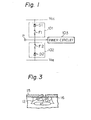
- FIG. 1 is a diagram of an electrostatic breakdown prevention circuit of an IC according to an embodiment of the present invention.
- the electrostatic breakdown prevention circuit (101, 102) of Fig. 1 is connected to a conductor connecting an input or output terminal P and an inner circuit of the IC.
- the circuit of Fig. 1 comprises a diode Dl and a fuse Fl series-connected between a power source V CC line having a voltage V CC and the conductor connecting terminal P to the inner circuit 103, and a fuse F2 and a diode D2 series-connected between the conductor connecting terminal P to the inner circuit'103 and a ground V EE line having a voltage V EE . Both fuses are connected on the side of the diode closest to the conductor connecting terminal P to the inner circuit 103.
- both the diodes Dl and D2 receive a backward bias voltage. Since the signal voltages at the input or output terminals of the IC have voltage values between V CC and V EE , the addition of the fuses and diodes has no effect on the static characteristics of the IC or on. the basic function thereof. When the terminal P receives an electrostatic surge voltage, however, the diodes Dl and D2 absorb electrostatic energy and act as protective elements to protect the inner circuit of the IC.
- the diodes Dl and D2 also work as elements having an electrostatic capacity, they decrease the operation speed of the IC.
- the decrease of the operation speed is very serious for a high-speed IC.
- the-fuses F1 and F2 are melted by applying a voltage slightly higher than the forward voltage drop of the_diodes Dl or D2 between the terminal P and the power source V CC line or ground VEE line. T hisdisconnects the diodes Dl and D2 from the terminal P. This technique enables one to use, as an electrostatic breakdown prevention element, an element with a high protection ability which would otherwise significantly reduce the operation speed of the IC.
- Figure 2 is a plan view of a pattern in the case where the electrostatic breakdown prevention circuit of Fig. 1 is formed on the semiconductor substrate of the IC using PN junction diodes.
- reference numeral 1 is the conductor pattern of the power source V CC
- 2 is a cathode contact hole of the diode D1 connected to the power source V CC line
- 3 is an N-type area isolated from the substrate for the diode Dl
- 4 is a metallized pattern of a bonding pad to connect the terminal P through a lead wire
- 5 is a P diffusion area for the diode Dl
- 6 is an anode contact hole of the diode D1
- 7 is a cover layer aperture for the fuse Fl
- 8 is a cover layer aperture for the bonding pad
- 9 is a pad area isolated from the substrate for the bonding pad
- 10 is a cover layer aperture for the fuse F2
- 11 is a cathode contact hole of the diode D2
- 12 is a P diffusion
- the fuses Fl and F2 are narrow patterns made of the same material as the wiring of the integrated circuit.
- the material is metal, polycrystalline silicon, or the like.
- PN junction diodes are shown as the diodes, Schottky diodes may be used instead.
- Figure 3 is a partial sectional view of the pattern of Fig. 2 along the line A-A. In the Figure, the hatched portion shows the conductor pattern.
- Reference numeral 16 shows an insulator layer.
- Reference symbol n + shows N-type semiconductor containing a larger amount of impurities, and n an N-type semiconductor containing a smaller amount of impurities.
- the P-type semiconductor of the P diffusion area 12 is used for the anode of the diode, and the N-type semiconductor is used for the cathode of the diode. While not shown in the Figure, generally the surface of the pattern is covered with a cover layer. The cover layer is taken off at bonding portions of the lead wires. On the fuses Fl and F2, the cover layer is also taken off, as shown by blocks of broken lines in Fig. 2, creating the cover layer apertures 7 and 10.
- the cover layer aperture on the fuse not only ensures that when the fuse melts, the fuse is easily broken by partial evaporation, but also prevents cracking of the cover layer. This therefore prevents deterioration of the reliability of the IC after the fuse is cut.
- the electrostatic breakdown prevention means in this embodiment, thyristors, transistors, or combination transistors, resistors, and the like can also be used.
- the fuses should withstand electrostatic energy small in quantity but high instantaneously in voltage and should be melted by heat due to electrical energy low in voltage but applied over a comparatively long time. So long as the above-mentioned characteristics are satisfied, the fuses may be made of any material in any form appropriate for the IC production process.
- An IC with electrostatic breakdown prevention circuits according to this embodiment may not be tested for dynamic characteristics, e.g., switching characteristics, before mounting, because the diodes Dl and D2 .are connected to the input or output terminals.
- dynamic characteristics e.g., switching characteristics, before mounting
- the dynamic characteristics of IC's belonging to the same production lot can be estimated by melting the fuses and then testing the characteristics of a sample chip from the identical lot.
- protection circuits in accordance with the present invention may be applied to a number of terminals of the same IC.
Landscapes
- Semiconductor Integrated Circuits (AREA)
- Design And Manufacture Of Integrated Circuits (AREA)
Applications Claiming Priority (2)
| Application Number | Priority Date | Filing Date | Title |
|---|---|---|---|
| JP227612/82 | 1982-12-28 | ||
| JP57227612A JPS59134863A (ja) | 1982-12-28 | 1982-12-28 | 静電破壊防止回路 |
Publications (2)
| Publication Number | Publication Date |
|---|---|
| EP0115143A2 true EP0115143A2 (fr) | 1984-08-08 |
| EP0115143A3 EP0115143A3 (fr) | 1986-01-08 |
Family
ID=16863659
Family Applications (1)
| Application Number | Title | Priority Date | Filing Date |
|---|---|---|---|
| EP83307627A Withdrawn EP0115143A3 (fr) | 1982-12-28 | 1983-12-15 | Circuit intégré comportant des circuits de protection contre le claquage électrostatique |
Country Status (2)
| Country | Link |
|---|---|
| EP (1) | EP0115143A3 (fr) |
| JP (1) | JPS59134863A (fr) |
Cited By (7)
| Publication number | Priority date | Publication date | Assignee | Title |
|---|---|---|---|---|
| GB2179494B (en) * | 1985-08-09 | 1989-07-26 | Plessey Co Plc | Protection structures for integrated circuits |
| EP0349890A3 (en) * | 1988-07-06 | 1990-10-24 | National Semiconductor Corporation | Esd low resistance input structure |
| EP0510900A3 (en) * | 1991-04-26 | 1993-02-10 | American Telephone And Telegraph Company | Wetting-based breakable links |
| WO1993008602A1 (fr) * | 1991-10-25 | 1993-04-29 | Thomson S.A. | Circuit de protection d'un instrument a semi-conducteurs contre la tension produite par les decharges d'electricite statique |
| EP0793272A3 (fr) * | 1996-02-29 | 2000-09-13 | STMicroelectronics, Inc. | Structure de protection comprenant une diode pour un plat de contact |
| WO2001047017A1 (fr) * | 1999-12-22 | 2001-06-28 | Koninklijke Philips Electronics N.V. | Circuit integre avec protection anti-esd amovible |
| US6753204B1 (en) * | 1997-09-30 | 2004-06-22 | Siemens Aktiengesellschaft | Method for assembling integrated circuits with protection of the circuits against electrostatic discharge |
Families Citing this family (2)
| Publication number | Priority date | Publication date | Assignee | Title |
|---|---|---|---|---|
| KR100337924B1 (ko) * | 2000-07-20 | 2002-05-24 | 박종섭 | 정전기 보호 회로 |
| US9184130B2 (en) * | 2012-10-05 | 2015-11-10 | Qualcomm Incorporated | Electrostatic protection for stacked multi-chip integrated circuits |
Family Cites Families (2)
| Publication number | Priority date | Publication date | Assignee | Title |
|---|---|---|---|---|
| USRE28481E (en) * | 1972-01-20 | 1975-07-15 | Semiconductor structure with fusible link and method | |
| US4426658A (en) * | 1980-12-29 | 1984-01-17 | Sprague Electric Company | IC With protection against reversed power supply |
-
1982
- 1982-12-28 JP JP57227612A patent/JPS59134863A/ja active Pending
-
1983
- 1983-12-15 EP EP83307627A patent/EP0115143A3/fr not_active Withdrawn
Cited By (7)
| Publication number | Priority date | Publication date | Assignee | Title |
|---|---|---|---|---|
| GB2179494B (en) * | 1985-08-09 | 1989-07-26 | Plessey Co Plc | Protection structures for integrated circuits |
| EP0349890A3 (en) * | 1988-07-06 | 1990-10-24 | National Semiconductor Corporation | Esd low resistance input structure |
| EP0510900A3 (en) * | 1991-04-26 | 1993-02-10 | American Telephone And Telegraph Company | Wetting-based breakable links |
| WO1993008602A1 (fr) * | 1991-10-25 | 1993-04-29 | Thomson S.A. | Circuit de protection d'un instrument a semi-conducteurs contre la tension produite par les decharges d'electricite statique |
| EP0793272A3 (fr) * | 1996-02-29 | 2000-09-13 | STMicroelectronics, Inc. | Structure de protection comprenant une diode pour un plat de contact |
| US6753204B1 (en) * | 1997-09-30 | 2004-06-22 | Siemens Aktiengesellschaft | Method for assembling integrated circuits with protection of the circuits against electrostatic discharge |
| WO2001047017A1 (fr) * | 1999-12-22 | 2001-06-28 | Koninklijke Philips Electronics N.V. | Circuit integre avec protection anti-esd amovible |
Also Published As
| Publication number | Publication date |
|---|---|
| JPS59134863A (ja) | 1984-08-02 |
| EP0115143A3 (fr) | 1986-01-08 |
Similar Documents
| Publication | Publication Date | Title |
|---|---|---|
| US4484244A (en) | Protection circuit for integrated circuit devices | |
| US4811155A (en) | Protection circuit for a semiconductor integrated circuit having bipolar transistors | |
| US5903424A (en) | Method for protecting an integrated circuit against electro-static discharges | |
| EP0260125A2 (fr) | Circuit de protection contre les décharges électrostatiques | |
| US20110079912A1 (en) | Connection for Off-Chip Electrostatic Discharge Protection | |
| US8035224B2 (en) | Semiconductor device | |
| JP5249768B2 (ja) | 低電圧線路を過電圧から保護するための集積回路 | |
| US5535084A (en) | Semiconductor integrated circuit having protection circuits | |
| EP0115143A2 (fr) | Circuit intégré comportant des circuits de protection contre le claquage électrostatique | |
| US6252256B1 (en) | Overvoltage protection circuit | |
| EP0215493A1 (fr) | Circuit à transistors MOS protégé | |
| US5805009A (en) | Method for operating an electrostatic discharge protection circuit | |
| NL8702918A (nl) | Beveiliging van geintegreerde schakelingen tegen elektrostatische ontladingen. | |
| US5334553A (en) | Telecommunication equipment protector | |
| US8373279B2 (en) | Die package | |
| EP0188378A2 (fr) | Dispositif à circuit semi-conducteur | |
| EP0042581B1 (fr) | Circuit intégré | |
| US6531744B2 (en) | Integrated circuit provided with overvoltage protection and method for manufacture thereof | |
| US4428066A (en) | Semiconductor read only memory | |
| US5627711A (en) | Self-protected semiconductor protection component | |
| US7429785B2 (en) | Stacked integrated circuit chip assembly | |
| EP0606667A1 (fr) | Dispositif semi-conducteur avec un circuit intégré pourvu de moyens de protection contre des surtensions | |
| EP0345432A1 (fr) | Diode pour la protection d'un circuit intégré contre les décharges électrostatiques | |
| EP0198468A2 (fr) | Dispositif de protection pour circuit intégré | |
| KR0134649B1 (ko) | 캐패시터를 구비한 반도체 패키지 및 그 제조방법 |
Legal Events
| Date | Code | Title | Description |
|---|---|---|---|
| PUAI | Public reference made under article 153(3) epc to a published international application that has entered the european phase |
Free format text: ORIGINAL CODE: 0009012 |
|
| AK | Designated contracting states |
Designated state(s): DE FR GB |
|
| PUAL | Search report despatched |
Free format text: ORIGINAL CODE: 0009013 |
|
| AK | Designated contracting states |
Designated state(s): DE FR GB |
|
| 17P | Request for examination filed |
Effective date: 19860217 |
|
| 17Q | First examination report despatched |
Effective date: 19870807 |
|
| STAA | Information on the status of an ep patent application or granted ep patent |
Free format text: STATUS: THE APPLICATION IS DEEMED TO BE WITHDRAWN |
|
| 18D | Application deemed to be withdrawn |
Effective date: 19880915 |
|
| RIN1 | Information on inventor provided before grant (corrected) |
Inventor name: EMORI, SHINJI |