EP0115175A2 - Bande élastomère de contacts encapsulés - Google Patents
Bande élastomère de contacts encapsulés Download PDFInfo
- Publication number
- EP0115175A2 EP0115175A2 EP83307830A EP83307830A EP0115175A2 EP 0115175 A2 EP0115175 A2 EP 0115175A2 EP 83307830 A EP83307830 A EP 83307830A EP 83307830 A EP83307830 A EP 83307830A EP 0115175 A2 EP0115175 A2 EP 0115175A2
- Authority
- EP
- European Patent Office
- Prior art keywords
- strip
- contacts
- contact
- mould
- conductor receiving
- Prior art date
- Legal status (The legal status is an assumption and is not a legal conclusion. Google has not performed a legal analysis and makes no representation as to the accuracy of the status listed.)
- Withdrawn
Links
Images


Classifications
-
- B—PERFORMING OPERATIONS; TRANSPORTING
- B29—WORKING OF PLASTICS; WORKING OF SUBSTANCES IN A PLASTIC STATE IN GENERAL
- B29C—SHAPING OR JOINING OF PLASTICS; SHAPING OF MATERIAL IN A PLASTIC STATE, NOT OTHERWISE PROVIDED FOR; AFTER-TREATMENT OF THE SHAPED PRODUCTS, e.g. REPAIRING
- B29C45/00—Injection moulding, i.e. forcing the required volume of moulding material through a nozzle into a closed mould; Apparatus therefor
- B29C45/0003—Injection moulding, i.e. forcing the required volume of moulding material through a nozzle into a closed mould; Apparatus therefor of successively moulded portions rigidly joined to each other
-
- H—ELECTRICITY
- H01—ELECTRIC ELEMENTS
- H01R—ELECTRICALLY-CONDUCTIVE CONNECTIONS; STRUCTURAL ASSOCIATIONS OF A PLURALITY OF MUTUALLY-INSULATED ELECTRICAL CONNECTING ELEMENTS; COUPLING DEVICES; CURRENT COLLECTORS
- H01R12/00—Structural associations of a plurality of mutually-insulated electrical connecting elements, specially adapted for printed circuits, e.g. printed circuit boards [PCB], flat or ribbon cables, or like generally planar structures, e.g. terminal strips, terminal blocks; Coupling devices specially adapted for printed circuits, flat or ribbon cables, or like generally planar structures; Terminals specially adapted for contact with, or insertion into, printed circuits, flat or ribbon cables, or like generally planar structures
- H01R12/70—Coupling devices
- H01R12/71—Coupling devices for rigid printing circuits or like structures
- H01R12/712—Coupling devices for rigid printing circuits or like structures co-operating with the surface of the printed circuit or with a coupling device exclusively provided on the surface of the printed circuit
- H01R12/716—Coupling device provided on the PCB
-
- H—ELECTRICITY
- H01—ELECTRIC ELEMENTS
- H01R—ELECTRICALLY-CONDUCTIVE CONNECTIONS; STRUCTURAL ASSOCIATIONS OF A PLURALITY OF MUTUALLY-INSULATED ELECTRICAL CONNECTING ELEMENTS; COUPLING DEVICES; CURRENT COLLECTORS
- H01R43/00—Apparatus or processes specially adapted for manufacturing, assembling, maintaining, or repairing of line connectors or current collectors or for joining electric conductors
- H01R43/02—Apparatus or processes specially adapted for manufacturing, assembling, maintaining, or repairing of line connectors or current collectors or for joining electric conductors for soldered or welded connections
-
- H—ELECTRICITY
- H01—ELECTRIC ELEMENTS
- H01R—ELECTRICALLY-CONDUCTIVE CONNECTIONS; STRUCTURAL ASSOCIATIONS OF A PLURALITY OF MUTUALLY-INSULATED ELECTRICAL CONNECTING ELEMENTS; COUPLING DEVICES; CURRENT COLLECTORS
- H01R43/00—Apparatus or processes specially adapted for manufacturing, assembling, maintaining, or repairing of line connectors or current collectors or for joining electric conductors
- H01R43/20—Apparatus or processes specially adapted for manufacturing, assembling, maintaining, or repairing of line connectors or current collectors or for joining electric conductors for assembling or disassembling contact members with insulating base, case or sleeve
- H01R43/24—Assembling by moulding on contact members
Definitions
- This invention relates, generally, to strip usage of contact members and more particularly, to encapsulation of contact members with an elastomeric substance such as silicone.
- a continuous strip of electrical contacts comprising a connecting portion and a mounting portion
- the strip comprises a continuously moulded carrier strip of elastomeric material having oppositely facing side walls and oppositely facing end walls, the connecting portions being moulded within the strip with connecting ends at an end wall of the strip and the mounting portion extending from the opposite end wall of the strip.
- the invention is advantageously applicable to contacts which comprise contact sockets, each having a conductor receiving end opening to a hollow conductor receiving body and a mounting portion at an end opposite to the conductor receiving end, the body being essentially perpendicular to the length of the strip with the conductor receiving end being at an end wall of the strip and the mounting portion extending from the opposite end wall of the strip.
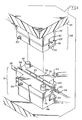
- a cavity mould shown generally at 20 has an inlet or spru 22 and which enters into a runner 24.
- the runner 24 is used for flow of the elastomeric strip material to the strip mould cavity as shown in Figures 3, 5, 7,8, 9 and 11.
- Heater wires 28 are arranged to keep the mould 20 at the desired temperature and a thermocouple 30 is inserted in a thermocouple mounting aperture 31 for sensing the temperature of the mould 20. Through suitable known circuitry the heater wires 28 positioned in the cavity mould 20 are controlled to ensure proper thermocycling of the mould 20.
- ejector pin retainer 32 is mounted in a channel below the row of apertures 23 and positions ejector pins 34 in registration with the aperture 23. The purpose of the ejector pins is to remove moulded product (not shown) from the mould 20 by upward movement of the pins 34 through the apertures 23.
- Mounting screws 36 are used to attach the ejector pin retainer 32 to an ejector block 40.
- Retainer ejector springs 38 are utilised to provide proper tension during the ejection cycle.
- a spacer 42 is located between the cavity mould 20 and the base 44, with the entire assembly being held together by retaining bolts 46.
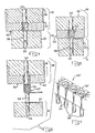
- FIG 2 there is shown an isometric, partially exploded view of the mating portion of the mould of the present invention.
- Components similar in structure and operation to components described in connection with Figure 1 will be identified by the previously assigned numeral with the addition of a prime (').
- Retainer bolts 46' pass through retaining bolt mounting holes 47' for fixedly holding the entire assembly together.
- a base 44' is utilised with a spacer 42' together with an ejector block 40' differing slightly in shape but performing a function similar to the ejector block 40 of Figure 1 and whose operation will be described in detail below.
- retainer springs 30' are utilised and have retainer spring sleeves 39 positioned therearound.
- Ejector pins 34' are utilised in conjunction with an ejector pin retainer 32', with the retainer 32' again being held in place by mounting screws 36'.
- Heater wires 28' are utilised with a thermocouple 30' disposed in the thermocouple mounting aperture 31' of the cavity mould 20 1 .
- a cavity mould upper plate 48 is mounted by use of cavity mould plate screws 52 to the cavity mould lower plates 50 with the entire assembly 48, 50 being mounted by mounting screws 36' to the cavity mould 20' and thereby forming a complete structure.
- FIG. 3 there is shown the apparatus of Figures 1 and 2 assembled in juxtaposition to eachother and ready for use in making the elastomeric strip of the present invention.
- the upper mould assembly shown generally at 49 which is comprised of the components from Figure 2 and which is mounted to a machine base 45 is positioned over the lower mould assembly shown generally at 51.
- the lower mould assembly 51 is comprised of the assembled components of Figure 1.
- an injector 54 which is utilised for injecting silicone 56 through the inlet 22 into the runner 24.
- contact sockets 58 Positioned in the runner 24 are contact sockets 58 which are placed in the runner 24.
- contact strip 60 In referring to Figures 1 through 6, and in particular Figures 3 through 6, construction of the contact strip 60 may be understood.
- Contact sockets 58 are inserted into the runner 24 such that the mounting portions 62 ( Figure 8) of the contact sockets 58 are inserted through contact spacing apertures 23 ( Figure 1).
- the upper and lower mould assemblies 49,51 are then mated.
- the injector 54 then injects silicone 56 through the inlet 22 into the runner 24.
- the heater wires 28,28' in conjunction with t, the thermocouples 30,30' maintain the temperature of their respective assemblies within suitable margins so as to ensure optimum temperature for the insertion and subsequent gelling or hardening of the silicone 56.
- the silicone 56 is injected into the runners 24 with sufficient pressure so as to ensure that substantially all voids are filled.
- the silicone 56 is then allowed to cure to a temperature sufficient so as to retain the shape of the mould and in the preferred embodiment of the present invention is at approximately 425 0 F although other temperatures can and may be used.
- the upper and lower mould assemblies 49,51 are then separated and through the use of the ejector pins 34, 34' the contact sockets 58 are removed from their respective portions of the mould, and a contact strip 60 is formed.
- the contact strip 60 is then advanced in the mould with a portion of the contact strip being reinserted into the mould such that a strip end 61 is reinserted into an end portion of the runner 24 and thereby the contact spacing apertures 23.
- Another set of contact sockets 58 is inserted into the remaining portion of runner 24 and the respective contact spacing apertures 23.
- the upper and lower mould assemblies 49,51 are closed with silicone 56 injected.
- the strip ends 61 are reinserted into the mould, the subsequent injection of silicone 56 allows a bond to be formed between the strip end 61 and the newly formed contact strip 60, thereby forming a continuous contact strip 60.
- the process is repeated forming a contact strip of any desirable or suitable length.
- FIG 7 there is shown a portion of a finished contact strip 60'.
- the contact strip 60' has contact strip notches 63 disposed therein and which are utilised for providing additional flexibility to the overall contact strips 60' as well as providing demarcation notches for insertion of the strip into a circuit board (shown in Figure 10).
- Notch forming ribs are suitably provided in the cavity of the upper mould 20' to this end.
- the contact socket 58 is comprised of a mounting portion 62, a conductor receiving end 64, and a hollow conductor receiving body 66 having conductor retaining tabs 65 contained therein.
- Silicone 56' completely encapsulates the upper portion of the contact socket 58 and therefore completely surrounds the hollow conductor receiving body 66 as well as completely filling the interior of the contact 58'.
- FIG 9 there is shown a long continuous strip of contact strips 60' which have been rolled onto a reel 68. Shown also is a nmumber of contacts separated from the continuous strip 60' and which are to be inserted into the circuit board 70. It is to be understood that fewer contacts or more contacts may be inserted without departing from the spirit and scope of the present invention. Shown also is a hand tool or insertion die 80 which is utilised to insert a contact strip 60' into the contact mounting hole 72 on the circuit board 70.
- the insertion die shown generally at 80 is comprised of end members 82 each of which has locating pins 84 which are inserted into contact mounting holes 72 thereby aligning the die 80 on the circuit board 70 (as shown in Figure 10).
- the die 80 has an upper contact strip retainer 86 and a lower contact strip 87 which are used to hold and retain a contact strip 60'.
- the upper and lower contact strip retainers 86,87 have ridges 88 which align with the contact strip notches 63. In this manner when a strip of contact strip 60' is inserted into the die 80, the centre-to-centre spacing between contact sockets 58' can be adjusted and/or corrected to coincide with the proper centre-to-centre spacing of the contact mounting holes 72.
- Retaining pins 90 hold the contact insertion bar 92 in place and are removed just prior to insertion of the contact strip 60' into the contact mounting holes 72' (shown in Figure 10).
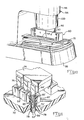
- FIG. 10 there is shown a contact strip 60' contained in the insertion die 80 ready to be inserted into the circuit board 70 by a press shown generally at 94.
- the press 94 has an upper arm 96 and a base 98 with a jaw 100 disposed in the upper arm 96.
- the jaw 100 moves vertically up or down in which thereby urges the contact insertion bar 92 vertically downward thereby forcing the contact sockets 58' contained in'the contact strip 60' into the contact mounting holes 72 contained in the circuit board 70.
- the movement of the jaw 100 is accomplished by use of a movable arm or lever (not shown) similar to that of a drill press although the jaw 100 does not rotate and which is readily obvious to one skilled in the art.
- FIG 11 there is shown an application of the present invention in conjunction with a circuit board 70' and an electronic component.
- the mounting portion 62' was placed through a contact mounting hole 72' and soldered 78 to a portion of a conductive path (not shown) disposed on the underside of the circuit board 70', although depending upon the contact chosen soldering may not be necessary.
- An integrated circuit 74 having integrated circuit pins 76 disposed thereon is mated with the contact sockets 58'. The integrated circuit pins 76 enter the conductor receiving end 64' into the hollow conductor receiving body 66' and make electrical contact with conductor retaining tabs 65'.
- the silicone 56' In that the interior of the contact socket 50' is completely filled with the silicone 56', insertion of the integrated circuit pin 76 forces the silicone 56' to be moved such that electrical contact is established between the integrated circuit pins 76 and the contact sockets 58' and in particular to the conductor retaining tab 65'. Upon removal of the integrated circuit 74, containing the integrated circuit pins 76, the silicone 56' in an elastomeric fashion returns to its original position thereby forming a substantially filled contact socket 58'. Therefore, the use of the silicone 56' in addition to providing the attributes necessary for a contact strip 60' also prevents the ingress of contaminants into the interior of the contact socket 58 as well as providing an environmental seal when a contact is in use.
- the disclosed invention produces a contact strip which is elastomeric i thereby allowing the placement of the contacts associated therewith into printed circuit boards or other similar devices having different hole-to-hole spacing. Additionally, the present invention produces a relatively inexpensive, easy to manufacture contact strip.
Landscapes
- Engineering & Computer Science (AREA)
- Manufacturing & Machinery (AREA)
- Mechanical Engineering (AREA)
- Coupling Device And Connection With Printed Circuit (AREA)
Applications Claiming Priority (2)
| Application Number | Priority Date | Filing Date | Title |
|---|---|---|---|
| US45331082A | 1982-12-27 | 1982-12-27 | |
| US453310 | 1982-12-27 |
Publications (2)
| Publication Number | Publication Date |
|---|---|
| EP0115175A2 true EP0115175A2 (fr) | 1984-08-08 |
| EP0115175A3 EP0115175A3 (fr) | 1985-12-04 |
Family
ID=23800038
Family Applications (1)
| Application Number | Title | Priority Date | Filing Date |
|---|---|---|---|
| EP83307830A Withdrawn EP0115175A3 (fr) | 1982-12-27 | 1983-12-21 | Bande élastomère de contacts encapsulés |
Country Status (2)
| Country | Link |
|---|---|
| EP (1) | EP0115175A3 (fr) |
| JP (1) | JPS59142956A (fr) |
Cited By (7)
| Publication number | Priority date | Publication date | Assignee | Title |
|---|---|---|---|---|
| EP0160387A1 (fr) * | 1984-03-26 | 1985-11-06 | Thomas & Betts Corporation | Barrette pour le maintien et la protection de contacts électriques |
| FR2587847A1 (fr) * | 1985-09-26 | 1987-03-27 | Thomas & Betts Corp | Dispositif modulaire pour le maintien, la pose et la protection de contacts femelles, a souder ou a braser sur une carte de circuit imprime |
| FR2590437A1 (fr) * | 1985-11-15 | 1987-05-22 | Sintra | Barrettes pour rattrapage des circuits imprimes |
| EP0193289A3 (fr) * | 1985-02-15 | 1988-01-07 | Crane Electronics, Inc. | Connecteur électrique |
| EP0418993A3 (en) * | 1989-09-19 | 1993-02-24 | Autosplice, Inc. | Continuous molded electronic component assembly |
| EP0753901A3 (fr) * | 1995-07-05 | 1997-07-09 | Autosplice Systems Inc | Connecteur électrique à moulage continu |
| EP3038214A1 (fr) * | 2014-12-23 | 2016-06-29 | Power Plus Communications AG | Support connecteur pour un composant électrique, en particulier un connecteur à fiches ou une antenne |
Family Cites Families (8)
| Publication number | Priority date | Publication date | Assignee | Title |
|---|---|---|---|---|
| US2977562A (en) * | 1954-12-08 | 1961-03-28 | Acme Wire Company | Dip soldered printed circuit sockets |
| DE2429714A1 (de) * | 1974-06-20 | 1976-01-08 | Daut & Rietz Kg | Anordnung zum anbringen von runden kontaktstiften od. dgl. in lochungen, insbesondere von leiterplatten |
| US4072376A (en) * | 1974-12-06 | 1978-02-07 | Amp Incorporated | Socket assemblies |
| FR2322465A1 (fr) * | 1975-08-29 | 1977-03-25 | Doloise Metallurgique | Dispositif de raccordement pour composants munis de fiches |
| FR2389254A1 (fr) * | 1977-04-25 | 1978-11-24 | Labinal | Procede de fabrication de boitiers isolants de connecteurs electriques |
| CH628484A5 (de) * | 1978-04-21 | 1982-02-26 | Erni & Co Elektro Ind | Verfahren und kontaktleiste zur herstellung gasdichter verbindungen fuer eine gedruckte rueckwandverdrahtung. |
| US4230387A (en) * | 1979-04-18 | 1980-10-28 | General Staple Company, Inc. | Continuous connector |
| DE2941770C2 (de) * | 1979-10-16 | 1982-11-04 | C.A. Weidmüller KG, 4930 Detmold | Verfahren und Vorrichtung zur Herstellung von Kontakten mit Crimpanschluß |
-
1983
- 1983-12-21 EP EP83307830A patent/EP0115175A3/fr not_active Withdrawn
- 1983-12-26 JP JP24436283A patent/JPS59142956A/ja active Pending
Cited By (8)
| Publication number | Priority date | Publication date | Assignee | Title |
|---|---|---|---|---|
| EP0160387A1 (fr) * | 1984-03-26 | 1985-11-06 | Thomas & Betts Corporation | Barrette pour le maintien et la protection de contacts électriques |
| EP0193289A3 (fr) * | 1985-02-15 | 1988-01-07 | Crane Electronics, Inc. | Connecteur électrique |
| USRE33005E (en) * | 1985-02-15 | 1989-08-01 | Crane Electronics, Inc. | Electrical connector |
| FR2587847A1 (fr) * | 1985-09-26 | 1987-03-27 | Thomas & Betts Corp | Dispositif modulaire pour le maintien, la pose et la protection de contacts femelles, a souder ou a braser sur une carte de circuit imprime |
| FR2590437A1 (fr) * | 1985-11-15 | 1987-05-22 | Sintra | Barrettes pour rattrapage des circuits imprimes |
| EP0418993A3 (en) * | 1989-09-19 | 1993-02-24 | Autosplice, Inc. | Continuous molded electronic component assembly |
| EP0753901A3 (fr) * | 1995-07-05 | 1997-07-09 | Autosplice Systems Inc | Connecteur électrique à moulage continu |
| EP3038214A1 (fr) * | 2014-12-23 | 2016-06-29 | Power Plus Communications AG | Support connecteur pour un composant électrique, en particulier un connecteur à fiches ou une antenne |
Also Published As
| Publication number | Publication date |
|---|---|
| EP0115175A3 (fr) | 1985-12-04 |
| JPS59142956A (ja) | 1984-08-16 |
Similar Documents
| Publication | Publication Date | Title |
|---|---|---|
| US4586607A (en) | Flexible strip of encapsulated contact members | |
| US4686766A (en) | Method of forming a flexible strip of encapsulated contact members | |
| EP0007762B1 (fr) | Dispositif et procédé pour enrober des composants électroniques dans des matières plastiques durcissables | |
| US4368168A (en) | Method for encapsulating electrical components | |
| US6219913B1 (en) | Connector producing method and a connector produced by insert molding | |
| US4250347A (en) | Method of encapsulating microelectronic elements | |
| EP0012532B1 (fr) | Connecteur électrique et méthode pour fabriquer une bande de connecteurs électriques | |
| CA2194208C (fr) | Support continu de pieces electriques ou mecaniques | |
| US8627563B2 (en) | Low pressure molding encapsulation of high voltage circuitry | |
| US4513942A (en) | Plate molding apparatus with interlocking cavity plates | |
| CA2037334A1 (fr) | Methode de moulage par injection de pieces a insert | |
| EP0115175A2 (fr) | Bande élastomère de contacts encapsulés | |
| CA1043974A (fr) | Methode d'encapsulation de composants electriques, et moule connexe | |
| US3672046A (en) | The method of making an electrical component | |
| US3539675A (en) | Method for encapsulating semiconductor devices | |
| US5828172A (en) | Diode mount for an led with a plug connector and compensating resistor, and a method of its manufacture | |
| US5879610A (en) | Method of making an electrical connector | |
| JPH1086188A (ja) | Ic用パッケージのモールド装置 | |
| EP0592768B1 (fr) | Procédé de surmoulage d'un insert métallique | |
| JP7346521B2 (ja) | プラグを製造するための方法および射出成形金型 | |
| GB2101516A (en) | Method of manufacture of plastics containers with incorporated heat sinks for integrated circuits and mould and heat sink combination for use with this method | |
| US3793709A (en) | Process for making a plastic-encapsulated semiconductor device | |
| JP3081835B1 (ja) | 電子回路コネクタ端子のインサート成形方法 | |
| US3799535A (en) | Carrier block and tray for use in encapsulation of semiconductor devices | |
| JP2939606B2 (ja) | 金属インサート樹脂成形法 |
Legal Events
| Date | Code | Title | Description |
|---|---|---|---|
| PUAI | Public reference made under article 153(3) epc to a published international application that has entered the european phase |
Free format text: ORIGINAL CODE: 0009012 |
|
| AK | Designated contracting states |
Designated state(s): BE DE FR GB IT NL |
|
| PUAL | Search report despatched |
Free format text: ORIGINAL CODE: 0009013 |
|
| RHK1 | Main classification (correction) |
Ipc: H01R 23/72 |
|
| AK | Designated contracting states |
Designated state(s): BE DE FR GB IT NL |
|
| 17P | Request for examination filed |
Effective date: 19860407 |
|
| 17Q | First examination report despatched |
Effective date: 19870205 |
|
| STAA | Information on the status of an ep patent application or granted ep patent |
Free format text: STATUS: THE APPLICATION IS DEEMED TO BE WITHDRAWN |
|
| 18D | Application deemed to be withdrawn |
Effective date: 19880503 |
|
| RIN1 | Information on inventor provided before grant (corrected) |
Inventor name: HANYEN, CLYDE KENNETH Inventor name: DUBBS, JACK FRANKLIN |