EP0115187A2 - Halbleiterspeicheranordnung mit Dekodiermitteln - Google Patents
Halbleiterspeicheranordnung mit Dekodiermitteln Download PDFInfo
- Publication number
- EP0115187A2 EP0115187A2 EP83307901A EP83307901A EP0115187A2 EP 0115187 A2 EP0115187 A2 EP 0115187A2 EP 83307901 A EP83307901 A EP 83307901A EP 83307901 A EP83307901 A EP 83307901A EP 0115187 A2 EP0115187 A2 EP 0115187A2
- Authority
- EP
- European Patent Office
- Prior art keywords
- stage
- decoder
- memory device
- semiconductor memory
- stage decoding
- Prior art date
- Legal status (The legal status is an assumption and is not a legal conclusion. Google has not performed a legal analysis and makes no representation as to the accuracy of the status listed.)
- Granted
Links
Images


Classifications
-
- G—PHYSICS
- G11—INFORMATION STORAGE
- G11C—STATIC STORES
- G11C8/00—Arrangements for selecting an address in a digital store
- G11C8/10—Decoders
-
- G—PHYSICS
- G11—INFORMATION STORAGE
- G11C—STATIC STORES
- G11C8/00—Arrangements for selecting an address in a digital store
- G11C8/12—Group selection circuits, e.g. for memory block selection, chip selection, array selection
Definitions
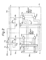
- one of the lower bits SA l1 of the internal address signal applied to the diodes llla to lllc is the low level, whereby almost all of the emitter current of the transistor 8 flows to one of the diodes llla to lllc.
- the base of the first transistor 12 in the inverter portion l a2 receives the bias voltage and the transistor 12 is turned on.
- a small emitter current of the transistor 12 flows to the ground through the resistor R4. Consequently, the third transistor 14 cannot be turned on, and the output signal SWL at the terminal 16 is the high level, which means non-selection of the word line.
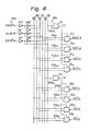
- the gate of the first-stage decoder when the gate of the first-stage decoder is not in operation, the power consumption of the set of the first-stage decoder gate and the corresponding second--stage decoder gates is almost zero. Only one set of a first-stage decoder gate and corresponding second-stage decoder gates in the memory device is powered upon an access command. In addition, when one set is activated, only the first-stage decoder gate and one of the second-stage decoder gates are powered. The other second-stage decoder gates are not powered. This means a considerable reduction in the power consumption of the decoder circuit.
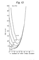
- the currents T 1 to I 5 and N are constant.
- the optimum number m of gates of the first-stage decoder can be obtained from equation (6).
- the number m must be an integer, the optimum number of gates of the first-stage decoder is determined as the integer nearest to the value given by equation (6).
Landscapes
- Engineering & Computer Science (AREA)
- Microelectronics & Electronic Packaging (AREA)
- Static Random-Access Memory (AREA)
- Semiconductor Memories (AREA)
Applications Claiming Priority (2)
| Application Number | Priority Date | Filing Date | Title |
|---|---|---|---|
| JP233906/82 | 1982-12-29 | ||
| JP57233906A JPS59124092A (ja) | 1982-12-29 | 1982-12-29 | メモリ装置 |
Publications (3)
| Publication Number | Publication Date |
|---|---|
| EP0115187A2 true EP0115187A2 (de) | 1984-08-08 |
| EP0115187A3 EP0115187A3 (en) | 1986-12-30 |
| EP0115187B1 EP0115187B1 (de) | 1991-02-20 |
Family
ID=16962433
Family Applications (1)
| Application Number | Title | Priority Date | Filing Date |
|---|---|---|---|
| EP83307901A Expired - Lifetime EP0115187B1 (de) | 1982-12-29 | 1983-12-22 | Halbleiterspeicheranordnung mit Dekodiermitteln |
Country Status (5)
| Country | Link |
|---|---|
| US (1) | US4617653A (de) |
| EP (1) | EP0115187B1 (de) |
| JP (1) | JPS59124092A (de) |
| DE (1) | DE3382163D1 (de) |
| IE (1) | IE56715B1 (de) |
Cited By (9)
| Publication number | Priority date | Publication date | Assignee | Title |
|---|---|---|---|---|
| EP0172112A3 (en) * | 1984-08-11 | 1988-02-24 | Fujitsu Limited | Semiconductor memory device |
| EP0282975A1 (de) * | 1987-03-16 | 1988-09-21 | Siemens Aktiengesellschaft | Mehrstufige integrierte Dekodereinrichtung |
| EP0202910A3 (en) * | 1985-05-20 | 1989-05-24 | Fujitsu Limited | Decoder circuit for a semiconductor memory device |
| EP0174845A3 (en) * | 1984-09-11 | 1989-08-16 | Fujitsu Limited | Semiconductor memory device |
| EP0193209A3 (en) * | 1985-02-28 | 1989-09-13 | Kabushiki Kaisha Toshiba | Semiconductor memory device |
| FR2656725A1 (de) * | 1989-12-29 | 1991-07-05 | Samsung Electronics Co Ltd | |
| FR2656727A1 (fr) * | 1989-12-29 | 1991-07-05 | Samsung Electronics Co Ltd | Matrice de cellules de memoire a semiconducteurs presentant une structure de lignes de mots interdigitee. |
| FR2656726A1 (fr) * | 1989-12-29 | 1991-07-05 | Samsung Electronics Co Ltd | Structure de lignes de mots interdigitees et croisees destinee a des memoires a semiconducteurs. |
| EP0509811A3 (en) * | 1991-04-18 | 1993-12-08 | Mitsubishi Electric Corp | Semiconductor memory device |
Families Citing this family (6)
| Publication number | Priority date | Publication date | Assignee | Title |
|---|---|---|---|---|
| US5257234A (en) * | 1987-07-15 | 1993-10-26 | Hitachi, Ltd. | Semiconductor integrated circuit device |
| EP0299697B1 (de) * | 1987-07-15 | 1993-09-29 | Hitachi, Ltd. | Integrierte Halbleiterschaltungsanordnung |
| EP0596198B1 (de) * | 1992-07-10 | 2000-03-29 | Sony Corporation | Flash-EPROM mit Löschprüfung und Architektur zum Adresszerhacken |
| JP2001126475A (ja) * | 1999-10-25 | 2001-05-11 | Mitsubishi Electric Corp | 半導体記憶装置 |
| US8755213B2 (en) | 2012-02-29 | 2014-06-17 | International Business Machines Corporation | Decoding scheme for bipolar-based diode three-dimensional memory requiring bipolar programming |
| US8842491B2 (en) | 2012-07-17 | 2014-09-23 | International Business Machines Corporation | Decoding scheme for bipolar-based diode three-dimensional memory requiring unipolar programming |
Family Cites Families (7)
| Publication number | Priority date | Publication date | Assignee | Title |
|---|---|---|---|---|
| US3599182A (en) * | 1969-01-15 | 1971-08-10 | Ibm | Means for reducing power consumption in a memory device |
| US3688280A (en) * | 1970-09-22 | 1972-08-29 | Ibm | Monolithic memory system with bi-level powering for reduced power consumption |
| US4027285A (en) * | 1973-12-26 | 1977-05-31 | Motorola, Inc. | Decode circuitry for bipolar random access memory |
| JPS528739A (en) * | 1975-07-10 | 1977-01-22 | Fujitsu Ltd | Electronic circuit |
| JPS5631137A (en) * | 1979-08-22 | 1981-03-28 | Fujitsu Ltd | Decoder circuit |
| JPS56112122A (en) * | 1980-02-08 | 1981-09-04 | Fujitsu Ltd | Decoder circuit |
| JPS5841597B2 (ja) * | 1980-12-24 | 1983-09-13 | 富士通株式会社 | 半導体メモリディスチャ−ジ回路 |
-
1982
- 1982-12-29 JP JP57233906A patent/JPS59124092A/ja active Granted
-
1983
- 1983-12-22 DE DE8383307901T patent/DE3382163D1/de not_active Expired - Lifetime
- 1983-12-22 EP EP83307901A patent/EP0115187B1/de not_active Expired - Lifetime
- 1983-12-28 US US06/566,323 patent/US4617653A/en not_active Expired - Fee Related
- 1983-12-29 IE IE3081/83A patent/IE56715B1/en not_active IP Right Cessation
Cited By (23)
| Publication number | Priority date | Publication date | Assignee | Title |
|---|---|---|---|---|
| EP0172112A3 (en) * | 1984-08-11 | 1988-02-24 | Fujitsu Limited | Semiconductor memory device |
| EP0174845A3 (en) * | 1984-09-11 | 1989-08-16 | Fujitsu Limited | Semiconductor memory device |
| US5097450A (en) * | 1985-02-28 | 1992-03-17 | Kabushiki Kaisha Toshiba | Semiconductor memory device having a plurality of memory blocks |
| EP0193209A3 (en) * | 1985-02-28 | 1989-09-13 | Kabushiki Kaisha Toshiba | Semiconductor memory device |
| EP0202910A3 (en) * | 1985-05-20 | 1989-05-24 | Fujitsu Limited | Decoder circuit for a semiconductor memory device |
| US4906994A (en) * | 1987-03-16 | 1990-03-06 | Siemens Aktiengelsellschaft | Multi-stage integrated decoder device |
| EP0282975A1 (de) * | 1987-03-16 | 1988-09-21 | Siemens Aktiengesellschaft | Mehrstufige integrierte Dekodereinrichtung |
| FR2656725A1 (de) * | 1989-12-29 | 1991-07-05 | Samsung Electronics Co Ltd | |
| FR2656727A1 (fr) * | 1989-12-29 | 1991-07-05 | Samsung Electronics Co Ltd | Matrice de cellules de memoire a semiconducteurs presentant une structure de lignes de mots interdigitee. |
| FR2656726A1 (fr) * | 1989-12-29 | 1991-07-05 | Samsung Electronics Co Ltd | Structure de lignes de mots interdigitees et croisees destinee a des memoires a semiconducteurs. |
| NL9000431A (nl) * | 1989-12-29 | 1991-07-16 | Samsung Electronics Co Ltd | Halfgeleidergeheugeninrichting. |
| US5583813A (en) * | 1991-04-18 | 1996-12-10 | Mitsubishi Denki Kabushiki Kaisha | Semiconductor memory device |
| US5544121A (en) * | 1991-04-18 | 1996-08-06 | Mitsubishi Denki Kabushiki Kaisha | Semiconductor memory device |
| US5559750A (en) * | 1991-04-18 | 1996-09-24 | Mitsubishi Denki Kabushiki Kaisha | Semiconductor memory device |
| EP0509811A3 (en) * | 1991-04-18 | 1993-12-08 | Mitsubishi Electric Corp | Semiconductor memory device |
| US5623454A (en) * | 1991-04-18 | 1997-04-22 | Mitsubishi Denki Kabushiki Kaisha | Semiconductor memory device |
| US5629895A (en) * | 1991-04-18 | 1997-05-13 | Mitsubishi Electric Engineering Co., Ltd. | Semiconductor memory device |
| US5650968A (en) * | 1991-04-18 | 1997-07-22 | Mitsubishi Denki Kabushiki Kaisha | Semiconductor memory device |
| US5652723A (en) * | 1991-04-18 | 1997-07-29 | Mitsubishi Denki Kabushiki Kaisha | Semiconductor memory device |
| EP0817198A1 (de) * | 1991-04-18 | 1998-01-07 | Mitsubishi Denki Kabushiki Kaisha | Halbleiterspeicheranordnung |
| US5848004A (en) * | 1991-04-18 | 1998-12-08 | Mitsubishi Denki Kabushiki Kaisha | Semiconductor memory device |
| US6026029A (en) * | 1991-04-18 | 2000-02-15 | Mitsubishi Denki Kabushiki Kaisha | Semiconductor memory device |
| US6356484B2 (en) | 1991-04-18 | 2002-03-12 | Mitsubishi Denki Kabushiki Kaisha | Semiconductor memory device |
Also Published As
| Publication number | Publication date |
|---|---|
| US4617653A (en) | 1986-10-14 |
| JPH0323995B2 (de) | 1991-04-02 |
| EP0115187B1 (de) | 1991-02-20 |
| IE833081L (en) | 1984-06-29 |
| EP0115187A3 (en) | 1986-12-30 |
| IE56715B1 (en) | 1991-11-20 |
| JPS59124092A (ja) | 1984-07-18 |
| DE3382163D1 (de) | 1991-03-28 |
Similar Documents
| Publication | Publication Date | Title |
|---|---|---|
| EP0115187A2 (de) | Halbleiterspeicheranordnung mit Dekodiermitteln | |
| US4104735A (en) | Arrangement for addressing a MOS store | |
| US5021688A (en) | Two stage address decoder circuit for semiconductor memories | |
| US4745582A (en) | Bipolar-transistor type random access memory device having redundancy configuration | |
| US4369503A (en) | Decoder circuit | |
| US4845678A (en) | Memory comprising simultaneously addressable memory elements | |
| US4385370A (en) | Decoder circuit | |
| US4347585A (en) | Reproduce only storage matrix | |
| EP0202892B1 (de) | Halbleiterspeichergerät mit Diodenmatrixdecodierer und Redundanzkonfiguration | |
| US4031413A (en) | Memory circuit | |
| JPS582437B2 (ja) | スリ−ステイト出力回路 | |
| US4986666A (en) | Semiconductor memory device | |
| EP0289893B1 (de) | BIPMOS-Dekodierschaltung | |
| US4730130A (en) | Writable array logic | |
| EP0090186B1 (de) | Komplementäre logische Schaltung | |
| JPH0310197B2 (de) | ||
| US5297084A (en) | Memory device with current mirror type sense amplifiers for comparing units of reference cells and information cells | |
| KR860001322B1 (ko) | 비손실 메모리 시스템 | |
| US4791382A (en) | Driver circuit | |
| US4697104A (en) | Two stage decoder circuit using threshold logic to decode high-order bits and diode-matrix logic to decode low-order bits | |
| US5117391A (en) | Bipolar memory cell array biasing technique with forward active PNP load cell | |
| US5467317A (en) | Semiconductor memory device for use an apparatus requiring high-speed access to memory cells | |
| US4783767A (en) | Static RAM with divided word-line structure | |
| US5444654A (en) | ROM with Bi-CMOS gate arrays | |
| US4899311A (en) | Clamping sense amplifier for bipolar ram |
Legal Events
| Date | Code | Title | Description |
|---|---|---|---|
| PUAI | Public reference made under article 153(3) epc to a published international application that has entered the european phase |
Free format text: ORIGINAL CODE: 0009012 |
|
| AK | Designated contracting states |
Designated state(s): DE FR GB |
|
| PUAL | Search report despatched |
Free format text: ORIGINAL CODE: 0009013 |
|
| AK | Designated contracting states |
Kind code of ref document: A3 Designated state(s): DE FR GB |
|
| 17P | Request for examination filed |
Effective date: 19870320 |
|
| 17Q | First examination report despatched |
Effective date: 19880218 |
|
| GRAA | (expected) grant |
Free format text: ORIGINAL CODE: 0009210 |
|
| AK | Designated contracting states |
Kind code of ref document: B1 Designated state(s): DE FR GB |
|
| REF | Corresponds to: |
Ref document number: 3382163 Country of ref document: DE Date of ref document: 19910328 |
|
| ET | Fr: translation filed | ||
| PLBE | No opposition filed within time limit |
Free format text: ORIGINAL CODE: 0009261 |
|
| STAA | Information on the status of an ep patent application or granted ep patent |
Free format text: STATUS: NO OPPOSITION FILED WITHIN TIME LIMIT |
|
| 26N | No opposition filed | ||
| PGFP | Annual fee paid to national office [announced via postgrant information from national office to epo] |
Ref country code: FR Payment date: 19951212 Year of fee payment: 13 |
|
| PGFP | Annual fee paid to national office [announced via postgrant information from national office to epo] |
Ref country code: GB Payment date: 19951213 Year of fee payment: 13 |
|
| PGFP | Annual fee paid to national office [announced via postgrant information from national office to epo] |
Ref country code: DE Payment date: 19951222 Year of fee payment: 13 |
|
| PG25 | Lapsed in a contracting state [announced via postgrant information from national office to epo] |
Ref country code: GB Effective date: 19961222 |
|
| GBPC | Gb: european patent ceased through non-payment of renewal fee |
Effective date: 19961222 |
|
| PG25 | Lapsed in a contracting state [announced via postgrant information from national office to epo] |
Ref country code: FR Effective date: 19970829 |
|
| PG25 | Lapsed in a contracting state [announced via postgrant information from national office to epo] |
Ref country code: DE Effective date: 19970902 |
|
| REG | Reference to a national code |
Ref country code: FR Ref legal event code: ST |