EP0116275B1 - Compensateur de puissance réactive - Google Patents
Compensateur de puissance réactive Download PDFInfo
- Publication number
- EP0116275B1 EP0116275B1 EP84100127A EP84100127A EP0116275B1 EP 0116275 B1 EP0116275 B1 EP 0116275B1 EP 84100127 A EP84100127 A EP 84100127A EP 84100127 A EP84100127 A EP 84100127A EP 0116275 B1 EP0116275 B1 EP 0116275B1
- Authority
- EP
- European Patent Office
- Prior art keywords
- capacitor
- discharge
- circuit
- thyristor switch
- reactive
- Prior art date
- Legal status (The legal status is an assumption and is not a legal conclusion. Google has not performed a legal analysis and makes no representation as to the accuracy of the status listed.)
- Expired
Links
Images
Classifications
-
- H—ELECTRICITY
- H02—GENERATION; CONVERSION OR DISTRIBUTION OF ELECTRIC POWER
- H02J—ELECTRIC POWER NETWORKS; CIRCUIT ARRANGEMENTS OR SYSTEMS FOR SUPPLYING OR DISTRIBUTING ELECTRIC POWER; SYSTEMS FOR STORING ELECTRIC ENERGY
- H02J3/00—Circuit arrangements for AC mains or AC distribution networks
- H02J3/18—Arrangements for adjusting, eliminating or compensating reactive power in networks
- H02J3/1821—Arrangements for adjusting, eliminating or compensating reactive power in networks using shunt compensators
- H02J3/1835—Arrangements for adjusting, eliminating or compensating reactive power in networks using shunt compensators with stepless control
- H02J3/1864—Arrangements for adjusting, eliminating or compensating reactive power in networks using shunt compensators with stepless control using reactive elements connected in series with semiconductor switches, e.g. static VAR compensators [SVC], thyristor-controlled reactors [TCR] or thyristor-switched capacitors [TSC]
-
- Y—GENERAL TAGGING OF NEW TECHNOLOGICAL DEVELOPMENTS; GENERAL TAGGING OF CROSS-SECTIONAL TECHNOLOGIES SPANNING OVER SEVERAL SECTIONS OF THE IPC; TECHNICAL SUBJECTS COVERED BY FORMER USPC CROSS-REFERENCE ART COLLECTIONS [XRACs] AND DIGESTS
- Y02—TECHNOLOGIES OR APPLICATIONS FOR MITIGATION OR ADAPTATION AGAINST CLIMATE CHANGE
- Y02E—REDUCTION OF GREENHOUSE GAS [GHG] EMISSIONS, RELATED TO ENERGY GENERATION, TRANSMISSION OR DISTRIBUTION
- Y02E40/00—Technologies for an efficient electrical power generation, transmission or distribution
- Y02E40/10—Flexible AC transmission systems [FACTS]
Definitions
- the invention is based on a reactive power compensator according to the preamble of patent claim 1.
- the invention relates to a prior art of reactive power compensators, as described in DE-PS 2303939.
- a compensation capacitor is precharged to the peak value of the mains AC voltage in the quarter period of the AC voltage preceding the switch-on time and connected to the AC network to be compensated by means of a thyristor switch via a choke when the voltage at the thyristor switch is approximately 0.
- the capacitor is discharged by firing the thyristor switch.
- the thyristor switch if the thyristor switch is closed, that is to say electrically conductive, and the capacitor is thus connected to the AC voltage network, the voltage across the capacitor corresponds to the network voltage at all times. If the capacitor is disconnected from the AC voltage supply by opening the thyristor switch, the thyristor switch takes over the capacitor voltage at the time of switching and subsequently, with the change in the capacitor voltage and the mains voltage, the differential voltage from both. The capacitor voltage decreases at least on average over time due to the discharge of the capacitor via the discharge circuit connected in parallel with it. As a rule, the capacitor is at zero current crossing, i.e. at the time of maximum mains voltage, separated from the AC mains.
- the capacitor must be able to discharge itself quickly enough via its discharge circuit, at the longest during half a period of the alternating voltage.
- the duration of half a period is 10 ms at an AC voltage frequency of 50 Hz.
- the capacitor usually has a capacitance on the order of a few 100 gF. In order for such a large capacity to discharge in 10 ms, the discharge circuit must have a low resistance.
- a purely ohmic resistance in the discharge circuit should e.g. are only a few Q, which in practice represents a short circuit with a correspondingly high power loss for the capacitor, which cannot be tolerated when the capacitor is connected to the AC network.
- This power loss can be limited by a switch arranged in the discharge circuit, primarily a fast-acting semiconductor switch, which is open when the capacitor is connected to the AC network and is only closed when the capacitor is disconnected from the AC network to initiate the discharge.
- a switch must be dimensioned for the full maximum mains voltage and is therefore also economically complex.
- the invention solves the problem of specifying a reactive power compensator which is subjected to low voltage loads and does not require any switching elements in the discharge circuit of the compensation capacitor.
- An advantage of the invention is that a rapid and continuous discharge of the capacitor, after it has been switched off from the AC voltage network, takes place in the discharge circuit of the capacitor without any fault-prone and expensive switching elements. This is achieved with simple means.
- a specially dimensioned iron choke coil can be used, with a second winding optionally being provided for particularly rapid magnetic reversal of the iron core.
- a specially dimensioned transformer with a short-circuit switch in its secondary circuit can also be used, which also enables very fast magnetic reversal and thus rapid discharge of the reactive load capacitor. This ensures that the valve voltage is relatively low and thus costs for expensive high voltage thyristors are saved.
- the destruction of thyristor valves can be avoided with certainty even in the event of a double misfire.
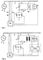
- N denotes a line of an electrical AC voltage network, which is fed by a generator G.
- a reactive power capacitor C is connected to the network N in series with a thyristor switch TS constructed, for example, from antiparallel thyristors.
- the ignition electrodes of the thyristors of the thyristor switch TS are connected to a first control unit SE 1 .
- These are electrical current, voltage and frequency signals M derived from the AC voltage network N ; Supplied, M ", mQ.
- the first control unit SE 1 generates from these signals in a known and therefore not further erläuteter manner in phase if necessary reactive power in the alternating-voltage network N ignition pulses for the thyristors of the thyristor switch TS.
- the capacitor C is a discharge circuit parallel connected, which has a discharge core choke D provided with an iron core as a variable reactance.
- the ohmic effective resistance of the choke winding is labeled R and shown separately from the discharge circuit choke D.
- the capacitor C forms a resonant circuit together with the discharge circuit choke D.
- This is a parallel resonant circuit in series with the thyristor switch TS on the AC voltage network N. If the thyristor switch TS is closed, at least one of the two antiparallel thyristors shown in FIG. 1 is conductive after ignition by the first control unit SE 1 , then the parallel resonant circuit becomes an oscillation with the Frequency of the AC voltage in the AC network N, ie the network frequency ⁇ N, forced.
- the behavior is the reverse of that of the resistors in the parallel branches.
- the discharge circuit choke D By using a sufficiently large inductance of the discharge circuit choke D, it can be achieved that the current in the capacitor branch i 1 exceeds the current in the choke branch i 2 by a few (for example 3 to 4) powers of ten. Compared to the reactive power occurring in the capacitor branch, the power loss in the choke branch, more precisely in the ohmic resistance R, is then of no importance.
- the discharge circuit of the capacitor C can therefore advantageously be permanently closed even during connection to the AC network. A switching element in the discharge circuit is unnecessary.
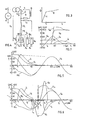
- FIG. 3 shows the magnetization characteristic of the iron core of the discharge circuit choke D.
- the induction foot ⁇ is plotted against the current i 2 through the discharge circuit choke D and, ideally, is composed of two straight line sections labeled 1 and 2. With small current values, the induction flow increases steeply (straight section 1). In this area, the iron core is unsaturated and the inductance of the discharge circuit choke D, which results from the slope of the straight section, is large. The iron core is saturated at a saturation current value i s . The induction flow ⁇ increases only slowly above this saturation current value i s .
- the aim should be to make the straight section 1 as steep as possible and to make the straight section 2 as flat as possible.
- the former can be achieved, among other things, by using a self-contained, approximately toroidal iron core. This largely eliminates the spread of the induction flux ⁇ .
- the latter can be achieved, among other things, by an even distribution of the choke winding over the iron core. As a result, the ratio of the number of turns to the length of the discharge circuit choke D, which also determines the size of the air inductance, is minimal.
- the saturation flow is preferably dimensioned to approximately 1.3 times the flow which flows through the discharge circuit choke D at the mains frequency (oN when the capacitor C is connected to the AC voltage network N.
- the saturation property of the discharge circuit choke D only comes into play as soon as the capacitor C is separated from the AC voltage network N by opening the thyristor switch TS. From this point in time, the oscillating circuit comprising capacitor C and discharge circuit choke D is no longer forced to oscillate at the mains frequency co N specified by the AC network N.
- the resonant circuit oscillates freely with its own frequency, ie its natural frequency ( OE further determined by the capacitance of the capacitor C, the inductance of the unsaturated discharge circuit choke D and the ohmic resistor R).
- the choke provides for the free, damped oscillation there is a smaller resistance than for the forced oscillation with the mains frequency ⁇ N. Since the capacitor C is separated from the AC mains N at maximum mains voltage, the maximum mains voltage is also at the capacitor C as the initial value of the free damped oscillation U N. Under these conditions the current through the En Charging circuit choke D in the free, damped oscillation significantly increases the current of the forced oscillation and drives the iron core of the discharge circuit choke D into saturation.
- the damping resistance R of the winding of the discharge circuit choke D is preferably selected so that the discharge of the capacitor corresponds to a RC discharge with aperiodic damping, with where L means the inductance of the discharge circuit choke D in the saturated region.
- the ohmic resistance R is preferably the effective resistance of the winding of the discharge circuit choke D, for which, for example, a material with a higher specific resistance than copper or aluminum is used.
- the discharge circuit inductor D acts as a variable reactance due to the saturation property of its iron core in the discharge circuit, which is larger when the capacitor C is connected to the AC voltage network N, ie when the thyristor switch TS is closed, than when the capacitor C is at open thyristor switch TS is separated from the AC network N.
- the difference between these two states is so significant that in the former case only a small, insignificant current i 2 flows in the discharge circuit, while in the second case a large current that discharges the capacitor C in less than half a period of the AC voltage i2 can flow.
- the discharge circuit can also be permanently closed. An interruption of the discharge circuit during the connection of the capacitor C to the AC network N is not necessary.
- An additional winding ZW is advantageously placed around the iron core of an unloading circuit choke D, as shown in FIG. 1, to which a device E for accelerated magnetic reversal of the iron core is connected. This is connected via a control line SY for synchronization with the first control unit SE 1 .
- the time period that elapses after the capacitor C is disconnected from the AC voltage network N and the free, damped oscillation sets in, until the current in the discharge circuit choke D has risen to such an extent that saturation occurs.
- a transformer TR is provided in the discharge circuit as a variable reactance. This is connected to the discharge circuit with a primary side.
- a controllable switching element SS is arranged in the secondary circuit of the transformer TR. With the controllable switching element SS, the secondary circuit of the transformer TR can be short-circuited and opened.
- the controllable switching element SS is preferably constructed from anti-parallel thyristors.
- the controllable switching element SS is assigned a second control unit SE 2 , which, like the first control unit SE 1 , generates ignition pulses for the thyristors. For synchronization, a second control unit SE 2 is coupled to the first control unit SE 1 .
- the second control unit SE 2 generates ignition pulses for the thyristors of the controllable switching element SS exactly when the first control unit SE 1 is not generating any ignition pulses for the thyristors of the thyristor switch TS and vice versa.
- the second control unit SE2 therefore only needs to negate the control signal of the first control unit SE 1 . This ensures that the controllable switching element SS is always open or closed in the opposite direction to the thyristor switch TS.
- This embodiment of the invention takes advantage of the fact that with an open secondary circuit of the transformer TR, the full inductance of the primary winding, the so-called no-load inductance, is effective in its primary circuit, whereas the so-called short-circuit or leakage impedance of the transformer is effective when the secondary circuit is closed.
- the transformer TR therefore acts with an open secondary circuit as a large reactance in the discharge circuit (during the connection of the capacitor C to the AC network), so that only a small current i 2 can flow in the discharge circuit, as explained above for the discharge circuit choke D.
- the transformer TR acts as a small reactance (if the capacitor is disconnected from the AC network N), so that, as also explained above for the discharge circuit choke, the capacitor C can quickly discharge through a free, damped oscillation.
- a switching element in the discharge circuit is unnecessary.
- the controllable switching element SS in the secondary circuit of the transformer TR offers the great advantage over a switching element in the discharge circuit that it only needs to be designed for a down-transformed and therefore much lower secondary voltage of the transformer TR.
- the capacitor C is connected to the AC network N via a transformer T.
- the discharge circuit reactor D is again connected with its active resistance R.
- an air throttle D L is connected to limit the valve current i rs in transient processes, the effective resistance of which is denoted by R L.
- the thyristor switch TS has two antiparallel connected thyristors V 1 and V 2 in parallel to a wiring capacitor BK.
- i TS and U rs denote the valve current and the valve voltage at the thyristor switch TS .
- a first varistor or surge arrester A 1 is connected in parallel with the series circuit comprising air throttle D L and thyristor switch TS, and a second varistor or surge arrester A 2 is connected in parallel with the thyristor switch TS.
- Both surge arresters A 1 and A 2 are voltage-dependent resistors made of a metal oxide, preferably of zinc oxide, whose resistance value decreases with increasing voltage from a predeterminable protection level or protective voltage value.
- the protection level of the first surge arrester A 1 is preferably greater than twice the amplitude of the mains voltage U N , which occurs on the secondary or low-voltage side of the transformer T.
- the level of protection of the second surge arrester A 2 is preferably the same or greater than the level of protection of the first surge arrester A 1 ; In terms of performance, however, the second surge arrester A 2 is designed to be weaker than the first surge arrester A 1 .
- the currents through the surge arrester A 1 and A 2 are denoted by i and i A1 A2, the chip which occur during current passage now g sab relay with UA1 and U AZ.
- FIG. 4 The effect of the circuit according to FIG. 4 is explained below with reference to FIGS. 5 to 7, in which the current i in kA and the voltage U in kV are plotted on the ordinate and the time t in ms is plotted on the abscissa (FIG. 5 and 6) or in a ⁇ s (Fig. 7).
- FIG. 5 shows when the compensation capacitor is switched off, the time profile of the sinusoidal mains voltage U N , the voltage U c of the reactive power capacitor C, the valve voltage U TS and the capacitor discharge current i 2 for the undisturbed case.
- the capacitor voltage U c is approximately constant and the capacitor discharge current i 2 is low, due to the high resistance of the discharge circuit choke D.
- the capacitor discharge current i 2 then rises sharply and discharges the capacitor C within a half-oscillation of the mains frequency ⁇ n .
- the maximum valve voltage U TS is only about 15% higher than the mains voltage amplitude.
- the capacitor C would discharge only very slowly, in accordance with the line shown in broken lines in FIG. 5. This would have the consequence that at the time of the minimum of the mains voltage U N the valve voltage U Ts would be approximately twice as large as the mains voltage amplitude. Relatively expensive thyristors with increased dielectric strength would have to be used for the thyristor switch TS or a plurality of thyristor switches TS would have to be connected in series. If misfiring of a thyristor now occurred at the worst time, the capacitor C would be recharged to a maximum of three times the mains voltage amplitude. The valve voltage U Ts would be reduced by the surge arresters A 1 and A 2 connected in parallel with the air throttle D L and the thyristor switch TS.
- the capacitor C is also recharged, as shown in FIG. 6. However, since the capacitor is almost discharged, it is only recharged to a maximum of twice the mains voltage amplitude.
- the valve voltage 0, and a negative valve current i Ts flows , which disappears approximately at time t 4 , then flows briefly in the opposite direction, cf. Fig. 7, and finally, approximately at the time point i 5 , versuhwindei, after which the current-carrying thyristor automatically switches back to the blocking state.
- the valve current i Ts simultaneously represents the charge-reversal current for the capacitor C.
- the frequency of the oscillation corresponds to the natural frequency of this series resonant circuit, which is set by means of the air choke D L in such a way that the thyristor switch TS does not result in an excessively steep rise and no excessive peak value of the valve current i Ts .
- this series resonant circuit is preferably matched to a harmonic of the mains current to be compensated.
- the oscillation is interrupted at time t 5 . Due to the high capacitor voltage at time t 5 and the relatively low mains voltage U N , a high valve voltage U TS and high valve voltages U A1 , U A2 occur. As a result, a remarkable arrester current i A1 flows in the first surge arrester A 1 between t 4 and t 5 . At the time t 5 , the arrester current i A2 also begins in the second surge arrester A 2 , which continues until the time t 7 and causes a reduction in the valve voltage U Ts .
- the iron core of the discharge circuit choke D is saturated again, in the opposite direction as at time t 1 , so that a strong capacitor discharge current i 2 sets in, which condenser C within half a period of the mains frequency up to time t 8 discharges.
- the valve voltage U Ts corresponds to the mains voltage U N , as in the undisturbed case according to FIG. 5.
- the thyristor V 2 If the thyristor V 2 is now misfired as long as the first surge arrester A 1 still carries the arrester current i A1 , it will commutate to the valve current path through V 2 and result in a current rise in it. If the steepness of the current rise outweighs the rate of propagation of the conductivity on the surface of the ignited thyristor V 2 , this could be destroyed by local overheating without protective measures.
- the air choke D L which limits the current rise, acts as a protective measure. With this embodiment of the invention, destruction of thyristor valves can be avoided with certainty even in the event of a double misfire.
- the AC voltage network N is shown as a single phase for the sake of simplicity.
- a compensation circuit corresponding to these figures must be provided for each phase.
- a thyristor switch TS instead of a thyristor switch TS, a plurality of thyristors can be connected in series and / or a plurality of thyristor switches TS can be provided in series with a thyristor switch TS, depending on the level of the AC voltage.
- inductive reactances as in the circuits according to FIGS. 1 and 2, can be provided in the discharge circuit of the capacitor C.
- the control units for the firing of the thyristors have been omitted in FIG. 4 for the sake of simplicity.
Landscapes
- Engineering & Computer Science (AREA)
- Power Engineering (AREA)
- Supply And Distribution Of Alternating Current (AREA)
- Ac-Ac Conversion (AREA)
- Control Of Electrical Variables (AREA)
Claims (10)
Applications Claiming Priority (2)
| Application Number | Priority Date | Filing Date | Title |
|---|---|---|---|
| EP83200196 | 1983-02-08 | ||
| EP83200196 | 1983-02-08 |
Publications (3)
| Publication Number | Publication Date |
|---|---|
| EP0116275A2 EP0116275A2 (fr) | 1984-08-22 |
| EP0116275A3 EP0116275A3 (en) | 1985-07-10 |
| EP0116275B1 true EP0116275B1 (fr) | 1987-07-15 |
Family
ID=8190928
Family Applications (1)
| Application Number | Title | Priority Date | Filing Date |
|---|---|---|---|
| EP84100127A Expired EP0116275B1 (fr) | 1983-02-08 | 1984-01-09 | Compensateur de puissance réactive |
Country Status (4)
| Country | Link |
|---|---|
| US (1) | US4567424A (fr) |
| EP (1) | EP0116275B1 (fr) |
| CA (1) | CA1213323A (fr) |
| DE (1) | DE3464828D1 (fr) |
Cited By (1)
| Publication number | Priority date | Publication date | Assignee | Title |
|---|---|---|---|---|
| DE19528766C1 (de) * | 1995-08-04 | 1997-01-16 | Siemens Ag | Thyristorgeschaltete Kondensatorbank |
Families Citing this family (26)
| Publication number | Priority date | Publication date | Assignee | Title |
|---|---|---|---|---|
| US4571535A (en) * | 1984-11-15 | 1986-02-18 | Westinghouse Electric Corp. | VAR Generator having controlled discharge of thyristor switched capacitors |
| DE3500786A1 (de) | 1985-01-11 | 1986-07-17 | Siemens AG, 1000 Berlin und 8000 München | Statischer blindleistungskompensator |
| US5032738A (en) * | 1986-01-22 | 1991-07-16 | Vithayathil John J | Scheme for rapid adjustment of network impedance |
| DE3616334C2 (de) * | 1986-05-15 | 2000-11-02 | Asea Brown Boveri | Verfahren zur Dämpfung mindestens einer elektrischen Oberschwingung zur Netzfrequenz in einem mehrphasigen Wechselstromnetz |
| US4727297A (en) * | 1986-07-17 | 1988-02-23 | Peak Systems, Inc. | Arc lamp power supply |
| DE4119707A1 (de) * | 1991-06-14 | 1992-12-17 | Siemens Ag | Verfahren zum herstellen eines hochtemperatur-supraleitenden bauteiles und hochtemperatur-supraleitendes bauteil |
| DE4215263C1 (fr) * | 1992-02-14 | 1993-04-29 | Grundfos A/S, Bjerringbro, Dk | |
| US5402057A (en) * | 1992-04-27 | 1995-03-28 | General Electric Co. | System and method for coordinating shunt reactance switching |
| US5402058A (en) * | 1992-12-09 | 1995-03-28 | General Electric Co. | Method and apparatus for controlling discharge of a thyristor-switched capacitor |
| US5469045A (en) * | 1993-12-07 | 1995-11-21 | Dove; Donald C. | High speed power factor controller |
| US5825162A (en) * | 1994-07-25 | 1998-10-20 | Hitachi, Ltd. | Electric power flow controller |
| US5670864A (en) * | 1995-05-26 | 1997-09-23 | Pacific Scientific Company | Adaptive automatic power capacitor for controlling controller a capacitor bank of a power distribution system |
| US5907234A (en) * | 1995-08-04 | 1999-05-25 | Siemens Aktiengesellschaft | Thyristor-switched capacitor bank |
| GB2307803B (en) * | 1995-11-28 | 2000-05-31 | Gec Alsthom Ltd | Three-phase static var compensator arrangement |
| FR2767610B1 (fr) * | 1997-08-21 | 1999-10-01 | Schneider Electric Sa | Dispositif de filtrage comportant un circuit de controle et appareil electrique comportant un tel dispositif |
| US5963021A (en) * | 1998-05-11 | 1999-10-05 | Siemens Power Transmission & Distribution, Llc | Delayed contact closing apparatus and method for capacitors |
| FI109946B (fi) * | 1998-07-07 | 2002-10-31 | Nokian Capacitors Oy | Purkauslaite |
| RU2308731C1 (ru) * | 2006-04-03 | 2007-10-20 | Людмила Прокопьевна Андрианова | Способ определения места однофазного замыкания на землю с использованием модели линий электропередачи в аварийном режиме |
| RU2316010C1 (ru) * | 2006-04-03 | 2008-01-27 | ООО "Инновационный центр при РГРТА" | Селективное устройство для определения однофазных замыканий в кабельных линиях |
| US7940029B2 (en) * | 2008-07-02 | 2011-05-10 | American Superconductor Corporation | Static VAR corrector |
| EP2577831B1 (fr) * | 2010-06-03 | 2019-03-06 | Vestas Wind Systems A/S | Procédé et agencement de commande pour la commande de condensateurs centraux dans des centrales éoliennes |
| CN102611090B (zh) * | 2011-01-19 | 2017-04-05 | 广州市金矢电子有限公司 | 电容脉冲放电装置、电容投切开关 |
| RU2561915C1 (ru) * | 2014-05-05 | 2015-09-10 | Федеральное государственное бюджетное образовательное учреждение высшего профессионального образования "Новосибирский государственный технический университет" | Способ регулирования напряжения узла электрической сети и узлов, примыкающих к нему |
| US9917463B2 (en) | 2015-09-25 | 2018-03-13 | General Electric Company | System and method for discharging a thyristor-switched capacitor |
| US11863062B2 (en) * | 2018-04-27 | 2024-01-02 | Raytheon Company | Capacitor discharge circuit |
| CN119906042B (zh) * | 2025-04-02 | 2025-07-04 | 德力西电气有限公司 | 一种无功补偿方法、系统、控制设备及存储介质 |
Family Cites Families (8)
| Publication number | Priority date | Publication date | Assignee | Title |
|---|---|---|---|---|
| DE616527C (de) * | 1931-11-06 | 1935-07-31 | Aeg | Einrichtung zur Kompensation der Leitungsinduktivitaet |
| US3187156A (en) * | 1961-07-25 | 1965-06-01 | Deutsche Edelstahlwerke Ag | Circuit for controlling the power of inductive heating or melting equipment |
| US3731183A (en) * | 1971-09-29 | 1973-05-01 | Inductotherm Corp | Power control and phase angle correcting apparatus |
| DE2303939C2 (de) * | 1973-01-24 | 1982-06-09 | Licentia Patent-Verwaltungs-Gmbh, 6000 Frankfurt | Verfahren zum Betrieb eines Blindstrom-Kompensationskondensators an einem Wechselstromnetz |
| CA1038450A (fr) * | 1973-10-09 | 1978-09-12 | Dennis A. Woodford | Controleur de reactance |
| US4210860A (en) * | 1978-09-15 | 1980-07-01 | Westinghouse Electric Corp. | VAR Generator with current sensitive inductance break point |
| US4292545A (en) * | 1979-04-16 | 1981-09-29 | Electric Power Research Institute, Inc. | Method and means for damping subsynchronous oscillations and DC offset in an AC power system |
| US4434376A (en) * | 1979-07-23 | 1984-02-28 | Electric Power Research Institute, Inc. | Method and means for damping subsynchronous oscillations and DC offset in an AC power system |
-
1984
- 1984-01-09 DE DE8484100127T patent/DE3464828D1/de not_active Expired
- 1984-01-09 EP EP84100127A patent/EP0116275B1/fr not_active Expired
- 1984-02-02 US US06/576,275 patent/US4567424A/en not_active Expired - Fee Related
- 1984-02-07 CA CA000446878A patent/CA1213323A/fr not_active Expired
Cited By (1)
| Publication number | Priority date | Publication date | Assignee | Title |
|---|---|---|---|---|
| DE19528766C1 (de) * | 1995-08-04 | 1997-01-16 | Siemens Ag | Thyristorgeschaltete Kondensatorbank |
Also Published As
| Publication number | Publication date |
|---|---|
| EP0116275A3 (en) | 1985-07-10 |
| US4567424A (en) | 1986-01-28 |
| CA1213323A (fr) | 1986-10-28 |
| DE3464828D1 (en) | 1987-08-20 |
| EP0116275A2 (fr) | 1984-08-22 |
Similar Documents
| Publication | Publication Date | Title |
|---|---|---|
| EP0116275B1 (fr) | Compensateur de puissance réactive | |
| DE69408811T2 (de) | Gleichstrom-Hochleistungsschalter | |
| DE2914313A1 (de) | Fehlerstrom-begrenzungsschaltung | |
| DE3333768A1 (de) | Vorrichtung zur begrenzung von wechselstroemen | |
| DE3444317C2 (de) | Reaktorschalter | |
| DE1806614A1 (de) | Folgeschalter fuer Hochspannungs-UEbertragungsanlagen | |
| DE2506021C2 (de) | Überspannungs-Schutzschaltungsanordnung für Hochleistungsthyristoren | |
| DE2513005B2 (de) | Netzgerät zur Transformation einer ungeregelten, pulsierenden Eingangsspannung in eine stabilisierte Gleichspannung | |
| DE3338301C2 (fr) | ||
| DE2127770B2 (de) | Gleichstrom Leistungsschalter | |
| DE1513155C3 (de) | UEberspannungsableiter | |
| EP1058488B1 (fr) | Circuit d'allumage pour lampe | |
| DE2208432B2 (de) | Leistungsschalteinrichtung | |
| DE2355603A1 (de) | Schutzschaltung | |
| DE69008836T2 (de) | Schaltungsanordnung, geeignet zum Zünden einer Hochdruckentladungslampe. | |
| DE2423646B2 (de) | Ueberspannungsableiter | |
| DE1213039B (de) | Anordnung zur Begrenzung von UEberstroemen | |
| DE2449548A1 (de) | Schutzanordnung fuer hauptthyristor vor vorwaerts-ueberspannung | |
| DE2407168A1 (de) | Leistungsschalteinrichtung | |
| DE3143622C2 (fr) | ||
| DE3542752C2 (fr) | ||
| DE4101963C1 (en) | Protective circuit counteracting mains interference pulses - has compensating capacitor with voltage rising at most to half max. interference voltage | |
| DE1262418B (de) | Einrichtung zur Begrenzung von UEberstroemen | |
| DE2362533A1 (de) | Elektrisches hochspannungsstarkstromnetz mit reihengeschalteten stabilisierungskondensatoren | |
| EP0242707A1 (fr) | Circuit de test |
Legal Events
| Date | Code | Title | Description |
|---|---|---|---|
| PUAI | Public reference made under article 153(3) epc to a published international application that has entered the european phase |
Free format text: ORIGINAL CODE: 0009012 |
|
| AK | Designated contracting states |
Designated state(s): AT BE CH DE FR GB IT LI LU NL SE |
|
| RBV | Designated contracting states (corrected) |
Designated state(s): CH DE LI SE |
|
| 17P | Request for examination filed |
Effective date: 19841010 |
|
| PUAL | Search report despatched |
Free format text: ORIGINAL CODE: 0009013 |
|
| AK | Designated contracting states |
Designated state(s): CH DE LI SE |
|
| 17Q | First examination report despatched |
Effective date: 19860925 |
|
| GRAA | (expected) grant |
Free format text: ORIGINAL CODE: 0009210 |
|
| AK | Designated contracting states |
Kind code of ref document: B1 Designated state(s): CH DE LI SE |
|
| REF | Corresponds to: |
Ref document number: 3464828 Country of ref document: DE Date of ref document: 19870820 |
|
| PLBE | No opposition filed within time limit |
Free format text: ORIGINAL CODE: 0009261 |
|
| STAA | Information on the status of an ep patent application or granted ep patent |
Free format text: STATUS: NO OPPOSITION FILED WITHIN TIME LIMIT |
|
| 26N | No opposition filed | ||
| PGFP | Annual fee paid to national office [announced via postgrant information from national office to epo] |
Ref country code: CH Payment date: 19900419 Year of fee payment: 7 |
|
| PG25 | Lapsed in a contracting state [announced via postgrant information from national office to epo] |
Ref country code: LI Effective date: 19910131 Ref country code: CH Effective date: 19910131 |
|
| REG | Reference to a national code |
Ref country code: CH Ref legal event code: PL |
|
| PGFP | Annual fee paid to national office [announced via postgrant information from national office to epo] |
Ref country code: SE Payment date: 19931222 Year of fee payment: 11 |
|
| PGFP | Annual fee paid to national office [announced via postgrant information from national office to epo] |
Ref country code: DE Payment date: 19940311 Year of fee payment: 11 |
|
| PG25 | Lapsed in a contracting state [announced via postgrant information from national office to epo] |
Ref country code: SE Effective date: 19950110 |
|
| EAL | Se: european patent in force in sweden |
Ref document number: 84100127.4 |
|
| PG25 | Lapsed in a contracting state [announced via postgrant information from national office to epo] |
Ref country code: DE Effective date: 19951003 |
|
| EUG | Se: european patent has lapsed |
Ref document number: 84100127.4 |