EP0117526A2 - Verfahren und Anordnung zum Sperren des Stromrichterbetriebs einer Umformervorrichtung - Google Patents
Verfahren und Anordnung zum Sperren des Stromrichterbetriebs einer Umformervorrichtung Download PDFInfo
- Publication number
- EP0117526A2 EP0117526A2 EP84101870A EP84101870A EP0117526A2 EP 0117526 A2 EP0117526 A2 EP 0117526A2 EP 84101870 A EP84101870 A EP 84101870A EP 84101870 A EP84101870 A EP 84101870A EP 0117526 A2 EP0117526 A2 EP 0117526A2
- Authority
- EP
- European Patent Office
- Prior art keywords
- absence
- voltage
- detecting
- valve
- detection signal
- Prior art date
- Legal status (The legal status is an assumption and is not a legal conclusion. Google has not performed a legal analysis and makes no representation as to the accuracy of the status listed.)
- Granted
Links
Images


Classifications
-
- H—ELECTRICITY
- H02—GENERATION; CONVERSION OR DISTRIBUTION OF ELECTRIC POWER
- H02M—APPARATUS FOR CONVERSION BETWEEN AC AND AC, BETWEEN AC AND DC, OR BETWEEN DC AND DC, AND FOR USE WITH MAINS OR SIMILAR POWER SUPPLY SYSTEMS; CONVERSION OF DC OR AC INPUT POWER INTO SURGE OUTPUT POWER; CONTROL OR REGULATION THEREOF
- H02M7/00—Conversion of AC power input into DC power output; Conversion of DC power input into AC power output
- H02M7/66—Conversion of AC power input into DC power output; Conversion of DC power input into AC power output with possibility of reversal
- H02M7/68—Conversion of AC power input into DC power output; Conversion of DC power input into AC power output with possibility of reversal by static converters
- H02M7/72—Conversion of AC power input into DC power output; Conversion of DC power input into AC power output with possibility of reversal by static converters using discharge tubes with control electrode or semiconductor devices with control electrode
- H02M7/75—Conversion of AC power input into DC power output; Conversion of DC power input into AC power output with possibility of reversal by static converters using discharge tubes with control electrode or semiconductor devices with control electrode using devices of a thyratron or thyristor type requiring extinguishing means
- H02M7/757—Conversion of AC power input into DC power output; Conversion of DC power input into AC power output with possibility of reversal by static converters using discharge tubes with control electrode or semiconductor devices with control electrode using devices of a thyratron or thyristor type requiring extinguishing means using semiconductor devices only
- H02M7/7575—Conversion of AC power input into DC power output; Conversion of DC power input into AC power output with possibility of reversal by static converters using discharge tubes with control electrode or semiconductor devices with control electrode using devices of a thyratron or thyristor type requiring extinguishing means using semiconductor devices only for high voltage direct transmission link
-
- H—ELECTRICITY
- H02—GENERATION; CONVERSION OR DISTRIBUTION OF ELECTRIC POWER
- H02M—APPARATUS FOR CONVERSION BETWEEN AC AND AC, BETWEEN AC AND DC, OR BETWEEN DC AND DC, AND FOR USE WITH MAINS OR SIMILAR POWER SUPPLY SYSTEMS; CONVERSION OF DC OR AC INPUT POWER INTO SURGE OUTPUT POWER; CONTROL OR REGULATION THEREOF
- H02M7/00—Conversion of AC power input into DC power output; Conversion of DC power input into AC power output
- H02M7/42—Conversion of DC power input into AC power output without possibility of reversal
- H02M7/44—Conversion of DC power input into AC power output without possibility of reversal by static converters
- H02M7/48—Conversion of DC power input into AC power output without possibility of reversal by static converters using discharge tubes with control electrode or semiconductor devices with control electrode
- H02M7/505—Conversion of DC power input into AC power output without possibility of reversal by static converters using discharge tubes with control electrode or semiconductor devices with control electrode using devices of a thyratron or thyristor type requiring extinguishing means
- H02M7/515—Conversion of DC power input into AC power output without possibility of reversal by static converters using discharge tubes with control electrode or semiconductor devices with control electrode using devices of a thyratron or thyristor type requiring extinguishing means using semiconductor devices only
- H02M7/525—Conversion of DC power input into AC power output without possibility of reversal by static converters using discharge tubes with control electrode or semiconductor devices with control electrode using devices of a thyratron or thyristor type requiring extinguishing means using semiconductor devices only with automatic control of output waveform or frequency
-
- Y—GENERAL TAGGING OF NEW TECHNOLOGICAL DEVELOPMENTS; GENERAL TAGGING OF CROSS-SECTIONAL TECHNOLOGIES SPANNING OVER SEVERAL SECTIONS OF THE IPC; TECHNICAL SUBJECTS COVERED BY FORMER USPC CROSS-REFERENCE ART COLLECTIONS [XRACs] AND DIGESTS
- Y02—TECHNOLOGIES OR APPLICATIONS FOR MITIGATION OR ADAPTATION AGAINST CLIMATE CHANGE
- Y02E—REDUCTION OF GREENHOUSE GAS [GHG] EMISSIONS, RELATED TO ENERGY GENERATION, TRANSMISSION OR DISTRIBUTION
- Y02E60/00—Enabling technologies; Technologies with a potential or indirect contribution to GHG emissions mitigation
- Y02E60/60—Arrangements for transfer of electric power between AC networks or generators via a high voltage DC link [HVCD]
Definitions
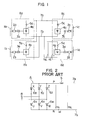
- the present invention relates to a method and a system for terminating inverter operation of a converting device having a bridge connection of thyristor valves and connected to a DC power transmission system, particularly a DC power transmission system having more than two terminals.
- Fig. 1 shows an example of a multi-terminal DC power transmission system, i.e., a DC power transmission system having more than two terminals.
- the converting stations 8a - 8d are interconnected by a pair of DC lines 7a, 7b forming a DC power transmission system, and are respectively connected to AC power transmission systems la, lb, lc, ld.
- Each converting station comprises a converting device 4a, 4b, 4c, 4d.
- each converting device The AC terminals of each converting device are connected to the AC power transmission system la, lb, lc, ld through a transformer 3a, 3b, 3c, 3d and an AC circuit breaker 2a, 2b, 2c, 2d.
- the DC terminals of each converting device are connected through a reactor 5a, 5b, 5c, 5d to the DC lines 7a and 7b.
- Each of the converting devices 4a - 4d comprises, as shown in Fig. 2, a bridge connection of thyristor valves 6u, 6v, 6w, 6x, 6y, 6z.
- the valves 6u, 6v, 6w. have one end connected to a negative line 7b, so that they are called valves of lower potential side.
- the valves 6x, 6y, 6z have one end connected (through a reactor 5a, 5b, 5c, 5d) to a positive line 7a so that they are called valves of higher potential side.
- Fig. 2 also shows AC terminals R, S, T for connection with three-phase AC power transmission system (la - ld in Fig.
- the converting device in one of the converting stations has been in the inverter operation and it is desired that the inverter operation of the converting device be terminated.
- the DC current through the converting apparatus 4d is reduced to zero, and upon detection or confirmation of the current being zero, gate pulses are blocked (in other words the converting device is gate-blocked).
- DC current i d flowing through the converting device contains, as shown in Fig. 3, ripples because of the DC voltage v d of the converting device and the DC line voltage v dL beyond the reactor 5d, so that it is very difficult to detect the current being zero.
- An object of the invention is to provide a method and a system for terminating the inverter operation of a converting device, which enable more reliable detection of the DC current being zero, and minimize the risk of an excessive current flowing through the converting device.
- a method for terminating inverter operation of a converting device connected to a DC power transmission system and having a bridge connection of thyristor valves comprising the steps of:
- a system for terminating inverter operation of a converting device connected to a DC power transmission system and having a bridge connection of thyristor valves comprising:
- Fig. 4 shows a converting device 4 similar to that shown in Fig. 2 and the converting device 4 similarly comprises a bridge connection of thyristor valves 6u - 6z.
- the AC terminals R, S, T and the DC terminals P, N may be similarly connected.
- voltage detection circuits 10u - 10z are provided in association with the thyristor valves 6u - 6z respectively.
- Each of the voltage detection circuits is provided with a first output terminal FV u - FV z and a second output terminal RV u - RV z , and produces a logic signal of "1" or forward voltage detection signal at the first terminal FV u - FV z when it detects a forward voltage across the associated thyristor valve 6u - 6z, and a logic signal of "1" or a reverse voltage detection signal at the terminal RV u - RV z when it detects a reverse voltage across the associated thyristor valve 6u - 6z.
- OR gates llu - llz are provided in association with the voltage detection circuits lOu - lOz, respectively. Each of the OR gates receives the forward voltage detection signal and the reverse voltage detection signal from the output terminals of the associated voltage detection circuit. Each of the OR gates llu - llz thus serves to detect non-conduction of the corresponding valve when either the forward voltage detection signal or the reverse voltage detection signal is being produced.
- An AND gate 12 is provided to receive signals from the OR gates llu - llw.
- Another AND gate 13 is provided to receive signals from the OR gates llx - llz.
- the output of the AND gate 12 is "1" if a voltage (forward or reverse) is present across each of the valves 6u - 6w of the lower potential side.
- the output of the AND gate 13 is "1" if a voltage is present across each of the valves 6x - 6z of the higher potential side.
- a further AND gate 14 is provided to receive output signals from the AND gates 12 and 13.
- the output signal of the AND gate 14 indicates absence of a current flowing through the converting device and is used as a condition for effecting termination of the inverter operation of the converting device, i.e., for blocking the gate pulses.
- the output signal of the AND gate 14 is inputted, together with a termination command TER to an AND gate 15.
- the output signal of the AND gate 15 is used to set an S-R type flip-flop 16, which is adapted to be reset by a start command STA.
- the output signal of the flip-flop 16 at the output terminal Q is "1" when the flip-flop 16 is set, and is inverted by an inverter 17.
- the output signal of the inverter 17 is fed to first terminals of AND gates 18u - 18z provided to receive, at second terminals, gate signals GS u - GS provided by a converting device control circuit 9 for the respective phases or valves.
- the output signals of the AND gates 18u - 18z are amplified by respective pulse amplifiers 19u - 19z and are then applied as gate pulses GP - GP z to the gates of the respective valves.
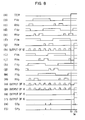
- Fig. 6(a) when the DC current i d of the converting device 4 is intermittent as shown in Fig. 6(a), the voltage V A-K across the anode and the cathode of a valve (any one of 6u - 6z) is as shown in Fig. 6(b).
- the various valves 6u - 6z have similar voltage waveforms V uA-K - V zA-K , but of different phases, as shown in Figs. 7(a) - (f).
- Fig. 7 also shows, at (g) - (r), logic signals outputted by the voltage detection circuits lOu - lOz.
- Fig. 8 shows signals at various parts of the circuitry of Fig. 5, before and after the production of termination command TER.
- a termination command TER is issued at a time point t 3 , when the W-phase valve 6w has just been fired and the W-phase valve 6w and the X-phase valve 6x are conducting,while the remaining valves are non-conducting.
- non-conduction of each of the valves is ascertained by detection of the presence of either forward or reverse voltage across the valve, and when all the valves are found to be non-conducting, absence of a current flowing through the converting device is detected or recognized, and gate pulses are blocked.
- the valves are kept non-conducting thereafter. Accordingly, the danager of an excessive current flowing through the converting device is minimized.
- detection is made to ascertain the presence of a forward or reverse voltage on all the valves in the lower potential side as well as all the valves in the higher potential side. But, the current must flow through at least one of the valves in the lower potential side and through at least one of the valves in the higher potential side. So that it is, in practice, sufficient to ascertain the presence of a voltage on all the valves of either the lower potential side or of the higher potential side.
- the AND gate 14 may therefore be replaced by an OR gate, or either the voltage detection circuits lOu - lOw for the lower potential side or the voltage detection circuits lOx - lOz for the higher potential side may be omitted.
- an ON-delay timer 20 may be inserted, as shown in Fig. 9, between the output terminal RV of the voltage detection circuit 10 (as representing lOu - lOz) and the OR gate 11 (as representing llu - llz). This is to make sure that the reverse voltage is applied on the thyristor for longer than the turn-off time of the thyristor, and the turn-off of the thyristor is completed, before the signal is actually applied to the OR gate 11 and the gate pulses are actually blocked.
- Such an ON delay timer may alternatively be inserted at the output of the OR gates llu - llz or at the output of the AND gates 12, 13.
- Fig. 10 shows a different arrangement for detecting the non-conduction of a valve.
- an S-R type flip-flop 22 is used for each valve, and the signal at the terminal RV is applied to a set input terminal S of the flip-flop 22.
- Applied to thu reset input terminal R is a gate signal GS to be supplied to the associated valve.
- the OR gate 11 is connected to receive the signal at the terminal RV and the signal at the terminal Q of the flip-flop 22 which is "1" when the flip-flop 22 is set.
- Fig. 11(a) - (e) The signals at various parts of the circuitry of Fig. 10 as connected to most of the circuitry of Figs. 4 and 5 are shown in Fig. 11(a) - (e).
- a gate pulse when a gate pulse is applied, the forward voltage disappears (or is kept absent). During such time that the forward voltage is not present, it is sufficient to detect presence of a reverse voltage to ascertain non-conduction of the valve.
- the embodiment of Fig. 10 is based on this concept, and utilizes a flip-flop 22 which is reset by the gate signal.
- the ouput of the OR gate 11 therefore indicates, when it is "1", that the associated valve is non-conducting.
- each valve may consist of a number of thyristors connected in series with each other. In such a case, a voltage across one or some of thyristors may be detected and used for the detection of the presence of the voltage across the valve.
- the converting device comprises only one bridge connection of thyristor valves. But it may alternatively comprise a plurality of bridge connections connected in series with each other.
Landscapes
- Engineering & Computer Science (AREA)
- Power Engineering (AREA)
- Inverter Devices (AREA)
- Rectifiers (AREA)
- Direct Current Feeding And Distribution (AREA)
Applications Claiming Priority (2)
| Application Number | Priority Date | Filing Date | Title |
|---|---|---|---|
| JP58032156A JPS59159629A (ja) | 1983-02-28 | 1983-02-28 | 変換装置の停止方法 |
| JP32156/83 | 1983-02-28 |
Publications (3)
| Publication Number | Publication Date |
|---|---|
| EP0117526A2 true EP0117526A2 (de) | 1984-09-05 |
| EP0117526A3 EP0117526A3 (en) | 1986-01-22 |
| EP0117526B1 EP0117526B1 (de) | 1988-08-24 |
Family
ID=12351055
Family Applications (1)
| Application Number | Title | Priority Date | Filing Date |
|---|---|---|---|
| EP84101870A Expired EP0117526B1 (de) | 1983-02-28 | 1984-02-22 | Verfahren und Anordnung zum Sperren des Stromrichterbetriebs einer Umformervorrichtung |
Country Status (5)
| Country | Link |
|---|---|
| US (1) | US4543492A (de) |
| EP (1) | EP0117526B1 (de) |
| JP (1) | JPS59159629A (de) |
| CA (1) | CA1201476A (de) |
| DE (1) | DE3473703D1 (de) |
Families Citing this family (2)
| Publication number | Priority date | Publication date | Assignee | Title |
|---|---|---|---|---|
| US4761563A (en) * | 1987-10-27 | 1988-08-02 | International Business Machines Corporation | Asynchronous multiphase switching gear |
| CN103119821B (zh) | 2010-09-30 | 2016-01-13 | Abb研究有限公司 | 多端hvdc系统的协调控制 |
Family Cites Families (10)
| Publication number | Priority date | Publication date | Assignee | Title |
|---|---|---|---|---|
| JPS4325041B1 (de) * | 1965-01-09 | 1968-10-29 | ||
| JPS4831015B1 (de) * | 1969-01-08 | 1973-09-26 | ||
| US3737763A (en) * | 1972-04-13 | 1973-06-05 | Gen Electric | Voltage distortion detection and control for hvdc converter |
| US3883791A (en) * | 1974-03-15 | 1975-05-13 | Mc Graw Edison Co | Three phase sequence insensitive full range SCR firing circuit |
| DE2637868B1 (de) * | 1975-04-30 | 1977-07-14 | Siemens Ag | Schutzschaltung fuer Thyristoren |
| JPS5332355A (en) * | 1976-09-06 | 1978-03-27 | Toshiba Corp | Control protecting for dc transmission system |
| US4177507A (en) * | 1978-03-22 | 1979-12-04 | General Electric Company | Method and control for maintaining optimum performance of HVDC power transmission systems at rectifier end during A. C. system fault |
| JPS5523023A (en) * | 1978-08-04 | 1980-02-19 | Tomofumi Tsujii | Exfoliating method for synthetic resin film of glass bottle |
| SU728210A1 (ru) * | 1978-09-11 | 1980-04-15 | Уральский ордена Трудового Красного Знамени политехнический институт им.С.М.Кирова | Автономный последовательный инвертор |
| JPS5746634A (en) * | 1980-09-04 | 1982-03-17 | Tokyo Electric Power Co | Controlling device for dc multiterminal transmission system |
-
1983
- 1983-02-28 JP JP58032156A patent/JPS59159629A/ja active Pending
-
1984
- 1984-02-17 CA CA000447736A patent/CA1201476A/en not_active Expired
- 1984-02-22 DE DE8484101870T patent/DE3473703D1/de not_active Expired
- 1984-02-22 EP EP84101870A patent/EP0117526B1/de not_active Expired
- 1984-02-24 US US06/583,362 patent/US4543492A/en not_active Expired - Fee Related
Also Published As
| Publication number | Publication date |
|---|---|
| DE3473703D1 (en) | 1988-09-29 |
| US4543492A (en) | 1985-09-24 |
| EP0117526A3 (en) | 1986-01-22 |
| CA1201476A (en) | 1986-03-04 |
| JPS59159629A (ja) | 1984-09-10 |
| EP0117526B1 (de) | 1988-08-24 |
Similar Documents
| Publication | Publication Date | Title |
|---|---|---|
| US11424694B2 (en) | Method for controlling shutdown wave blocking of multilevel inverter circuit and application thereof | |
| US11632060B2 (en) | Power conversion device | |
| US11070124B2 (en) | Power conversion device | |
| US10819217B2 (en) | Power conversion device and communication method | |
| US4837671A (en) | State signal formation for indicating the transition into the bypass mode of operation in an apparatus for high-voltage D-C transmission | |
| US20160006368A1 (en) | Power Converter | |
| US11621650B2 (en) | Method for current limitation in the event of transient voltage variations at an AC output of a multi-level inverter and a multi-level inverter | |
| EP0298515B1 (de) | Gattersteuerungsanordnung für ein Thyristorventil | |
| US4320445A (en) | Gate control circuit for thyristor converter | |
| US4543492A (en) | Method and system for terminating operation of an HVDC invertor | |
| US20260112957A1 (en) | Power Conversion System and Control Device for Same | |
| US3761733A (en) | Arrangement for uninterruptable power supply to a load from two or more a.c. power sources | |
| EP4099557A1 (de) | Steuerschaltung für einen dreipegelwandler vom npc-typ, dreipegelwandler vom npc-typ und windkraftanlage | |
| US4908756A (en) | Detecting apparatus for abnormality in inverter circuit | |
| US5025360A (en) | Inverter switch with parallel free-wheel diodes | |
| US5010470A (en) | Current balancing structure for semiconductor switching devices | |
| CA2230260C (en) | A method for communication between a low potential level and a valve located on high voltage potential in a high voltage converter station as well as a device for such a communication | |
| US4685045A (en) | Device for failure detection in series-connected semiconductor rectifiers | |
| JP7266373B2 (ja) | 電力変換装置 | |
| US4449088A (en) | Commutation failure correction scheme for a controlled current inverter | |
| US3401326A (en) | Three phase inverter circuit having three stage ring counter and power inverters with ferro-resonant wave shaping circuits | |
| CN108551281A (zh) | 一种无刷直流电机精确换相的方法及装置 | |
| EP4542842A1 (de) | Elektrische leistungsumwandlungsvorrichtung und steuerungsverfahren dafür | |
| JP6765588B1 (ja) | 電力変換システム | |
| SU983946A1 (ru) | Транзисторный преобразователь |
Legal Events
| Date | Code | Title | Description |
|---|---|---|---|
| PUAI | Public reference made under article 153(3) epc to a published international application that has entered the european phase |
Free format text: ORIGINAL CODE: 0009012 |
|
| 17P | Request for examination filed |
Effective date: 19840320 |
|
| AK | Designated contracting states |
Designated state(s): CH DE LI SE |
|
| PUAL | Search report despatched |
Free format text: ORIGINAL CODE: 0009013 |
|
| AK | Designated contracting states |
Designated state(s): CH DE LI SE |
|
| 17Q | First examination report despatched |
Effective date: 19870317 |
|
| GRAA | (expected) grant |
Free format text: ORIGINAL CODE: 0009210 |
|
| AK | Designated contracting states |
Kind code of ref document: B1 Designated state(s): CH DE LI SE |
|
| REF | Corresponds to: |
Ref document number: 3473703 Country of ref document: DE Date of ref document: 19880929 |
|
| PLBE | No opposition filed within time limit |
Free format text: ORIGINAL CODE: 0009261 |
|
| STAA | Information on the status of an ep patent application or granted ep patent |
Free format text: STATUS: NO OPPOSITION FILED WITHIN TIME LIMIT |
|
| 26N | No opposition filed | ||
| PGFP | Annual fee paid to national office [announced via postgrant information from national office to epo] |
Ref country code: CH Payment date: 19920224 Year of fee payment: 9 |
|
| PG25 | Lapsed in a contracting state [announced via postgrant information from national office to epo] |
Ref country code: LI Effective date: 19930228 Ref country code: CH Effective date: 19930228 |
|
| REG | Reference to a national code |
Ref country code: CH Ref legal event code: PL |
|
| EAL | Se: european patent in force in sweden |
Ref document number: 84101870.8 |
|
| PGFP | Annual fee paid to national office [announced via postgrant information from national office to epo] |
Ref country code: SE Payment date: 19950215 Year of fee payment: 12 |
|
| PGFP | Annual fee paid to national office [announced via postgrant information from national office to epo] |
Ref country code: DE Payment date: 19950222 Year of fee payment: 12 |
|
| PG25 | Lapsed in a contracting state [announced via postgrant information from national office to epo] |
Ref country code: SE Effective date: 19960223 |
|
| PG25 | Lapsed in a contracting state [announced via postgrant information from national office to epo] |
Ref country code: DE Effective date: 19961101 |