EP0118054A1 - Dispositif d'alimentation à commutation avec entrée en tension continue - Google Patents
Dispositif d'alimentation à commutation avec entrée en tension continue Download PDFInfo
- Publication number
- EP0118054A1 EP0118054A1 EP84101323A EP84101323A EP0118054A1 EP 0118054 A1 EP0118054 A1 EP 0118054A1 EP 84101323 A EP84101323 A EP 84101323A EP 84101323 A EP84101323 A EP 84101323A EP 0118054 A1 EP0118054 A1 EP 0118054A1
- Authority
- EP
- European Patent Office
- Prior art keywords
- output
- input
- voltage
- output voltage
- switch
- Prior art date
- Legal status (The legal status is an assumption and is not a legal conclusion. Google has not performed a legal analysis and makes no representation as to the accuracy of the status listed.)
- Granted
Links
- 239000003990 capacitor Substances 0.000 claims abstract description 7
- 238000004804 winding Methods 0.000 claims description 15
- 230000005540 biological transmission Effects 0.000 claims description 2
- 230000001939 inductive effect Effects 0.000 claims description 2
- 238000002955 isolation Methods 0.000 description 4
- 238000010586 diagram Methods 0.000 description 3
- 239000004065 semiconductor Substances 0.000 description 3
- 230000000694 effects Effects 0.000 description 2
- XUIMIQQOPSSXEZ-UHFFFAOYSA-N Silicon Chemical compound [Si] XUIMIQQOPSSXEZ-UHFFFAOYSA-N 0.000 description 1
- 230000015556 catabolic process Effects 0.000 description 1
- 238000010276 construction Methods 0.000 description 1
- 230000003247 decreasing effect Effects 0.000 description 1
- 238000009499 grossing Methods 0.000 description 1
- 238000000034 method Methods 0.000 description 1
- 238000012544 monitoring process Methods 0.000 description 1
- 229910052710 silicon Inorganic materials 0.000 description 1
- 239000010703 silicon Substances 0.000 description 1
- 239000003381 stabilizer Substances 0.000 description 1
- 230000000087 stabilizing effect Effects 0.000 description 1
Images


Classifications
-
- H—ELECTRICITY
- H02—GENERATION; CONVERSION OR DISTRIBUTION OF ELECTRIC POWER
- H02M—APPARATUS FOR CONVERSION BETWEEN AC AND AC, BETWEEN AC AND DC, OR BETWEEN DC AND DC, AND FOR USE WITH MAINS OR SIMILAR POWER SUPPLY SYSTEMS; CONVERSION OF DC OR AC INPUT POWER INTO SURGE OUTPUT POWER; CONTROL OR REGULATION THEREOF
- H02M1/00—Details of apparatus for conversion
- H02M1/36—Means for starting or stopping converters
-
- H—ELECTRICITY
- H02—GENERATION; CONVERSION OR DISTRIBUTION OF ELECTRIC POWER
- H02M—APPARATUS FOR CONVERSION BETWEEN AC AND AC, BETWEEN AC AND DC, OR BETWEEN DC AND DC, AND FOR USE WITH MAINS OR SIMILAR POWER SUPPLY SYSTEMS; CONVERSION OF DC OR AC INPUT POWER INTO SURGE OUTPUT POWER; CONTROL OR REGULATION THEREOF
- H02M3/00—Conversion of DC power input into DC power output
- H02M3/02—Conversion of DC power input into DC power output without intermediate conversion into AC
- H02M3/04—Conversion of DC power input into DC power output without intermediate conversion into AC by static converters
- H02M3/10—Conversion of DC power input into DC power output without intermediate conversion into AC by static converters using discharge tubes with control electrode or semiconductor devices with control electrode
- H02M3/145—Conversion of DC power input into DC power output without intermediate conversion into AC by static converters using discharge tubes with control electrode or semiconductor devices with control electrode using devices of a triode or transistor type requiring continuous application of a control signal
- H02M3/155—Conversion of DC power input into DC power output without intermediate conversion into AC by static converters using discharge tubes with control electrode or semiconductor devices with control electrode using devices of a triode or transistor type requiring continuous application of a control signal using semiconductor devices only
-
- H—ELECTRICITY
- H02—GENERATION; CONVERSION OR DISTRIBUTION OF ELECTRIC POWER
- H02M—APPARATUS FOR CONVERSION BETWEEN AC AND AC, BETWEEN AC AND DC, OR BETWEEN DC AND DC, AND FOR USE WITH MAINS OR SIMILAR POWER SUPPLY SYSTEMS; CONVERSION OF DC OR AC INPUT POWER INTO SURGE OUTPUT POWER; CONTROL OR REGULATION THEREOF
- H02M3/00—Conversion of DC power input into DC power output
- H02M3/22—Conversion of DC power input into DC power output with intermediate conversion into AC
- H02M3/24—Conversion of DC power input into DC power output with intermediate conversion into AC by static converters
- H02M3/28—Conversion of DC power input into DC power output with intermediate conversion into AC by static converters using discharge tubes with control electrode or semiconductor devices with control electrode to produce the intermediate AC
- H02M3/325—Conversion of DC power input into DC power output with intermediate conversion into AC by static converters using discharge tubes with control electrode or semiconductor devices with control electrode to produce the intermediate AC using devices of a triode or a transistor type requiring continuous application of a control signal
- H02M3/335—Conversion of DC power input into DC power output with intermediate conversion into AC by static converters using discharge tubes with control electrode or semiconductor devices with control electrode to produce the intermediate AC using devices of a triode or a transistor type requiring continuous application of a control signal using semiconductor devices only
- H02M3/337—Conversion of DC power input into DC power output with intermediate conversion into AC by static converters using discharge tubes with control electrode or semiconductor devices with control electrode to produce the intermediate AC using devices of a triode or a transistor type requiring continuous application of a control signal using semiconductor devices only in push-pull configuration
- H02M3/3376—Conversion of DC power input into DC power output with intermediate conversion into AC by static converters using discharge tubes with control electrode or semiconductor devices with control electrode to produce the intermediate AC using devices of a triode or a transistor type requiring continuous application of a control signal using semiconductor devices only in push-pull configuration with automatic control of output voltage or current
- H02M3/3378—Conversion of DC power input into DC power output with intermediate conversion into AC by static converters using discharge tubes with control electrode or semiconductor devices with control electrode to produce the intermediate AC using devices of a triode or a transistor type requiring continuous application of a control signal using semiconductor devices only in push-pull configuration with automatic control of output voltage or current in a push-pull configuration of the parallel type
Definitions
- the invention relates to a clocked supply device with DC voltage input, which contains a pulse width modulator controlled by the output voltage and at least one switch actuated by the latter, and on the output side a low-pass filter constructed from an inductance and a capacitance.
- a DC voltage at the input is chopped by the switch and the AC voltage thus generated is smoothed by the low-pass filter on the output side.
- the pulse width modulator is controlled by feedback in such a way that the output voltage approximately maintains a predetermined setpoint.
- Such clocked supply devices are used to generate constant DC voltage from a possibly fluctuating DC voltage with a high degree of efficiency, which, e.g. suitable for supplying electronic devices.
- a clocked supply device (buck controller) is known according to the preamble of claim 1 (International Semiconductor Databook 1981, pp. 731-733 from Unitrode Corporation or U. Tietze, Ch. Schenk: Semiconductor Circuitry, 5th Edition, p. 391-394, Springer-Verlag 1980), in which a switch actuated by the pulse width modulator lies between the input and the low-pass filter and a free-wheeling diode connects the input of the low-pass filter to the zero point, eg earth.
- a clocked power supply is known (International Semiconductor Databook 1981, pp. 733, 734), which contains a transformer with symmetrical primary and secondary windings, the middle connection of the primary winding having a DC input and the outer connections are each connected to earth via a switch actuated by the pulse width modulator, while the secondary winding, together with two diodes, forms a full-wave rectifier, the output of which is connected to the input of the low-pass filter.
- the inductance of the low-pass filter limits the speed of the current rise to a maximum value permissible for the circuit to function correctly. If an input voltage is applied to the de-energized power supply, the current through the inductor increases only slowly, the capacitance of the low-pass filter is charged accordingly slowly and the output voltage reaches its setpoint with a considerable delay, which is greater, the lower the frequency of the Chopper and the higher the dynamics of the load current, which must be coped with if the output voltage is constant and the larger the components of the low-pass filter are dimensioned.
- An application in which such requirements occur is e.g. the power supply of devices for monitoring a line (e.g. measuring transducers), or auxiliary devices of such devices, from the line to be monitored.
- a line e.g. measuring transducers
- auxiliary devices of such devices from the line to be monitored.
- the invention seeks to remedy this.
- the invention as characterized in the claims, solves the problem of creating a generic clocked supply device in which the output voltage, after application of an input voltage, reaches its setpoint at least approximately with very little delay.
- the advantages of the invention are essentially achieved in that the inductance of the low-pass filter in a generic supply device is bridged by a bridging circuit, the impedance of which has at most a low inductive component in comparison with said inductance and which conducts if the output voltage is below a minimum value, which is not higher than the nominal value of the same, lies and otherwise does not conduct.
- the capacity of the low-pass filter is quickly charged by applying a rapidly increasing, high charging current after an input voltage has been applied, until the selected minimum value of the output voltage is reached. As soon as sufficient current flows through the inductance of the low-pass filter to maintain this minimum value, the bypass circuit no longer conducts.
- a clocked power supply device which in its basic structure contains a pulse width modulator 1 of a commercial type (e.g. SG 1225A from Silicon General), which, controlled by the output voltage, actuates a switch 2 at input 3, which has a low-pass filter on the output side is connected downstream, consisting of an inductor 5 located between the switch 2 and the output 4 and a capacitance 6 located between the output 4 and earth.
- the input of the low-pass filter is connected to earth via a free-wheeling diode 7.
- the inductance 5 is bridged by a bridging circuit 8.
- This contains an impedance, which in its simplest form is a resistor 9 is formed and a switch 10 which is actuated by a comparator 11 which compares the output voltage with a reference voltage present at the reference input 12.
- Switch 2 controlled by pulse width modulator 1, opens periodically for the duration of an interval, the length of which depends on the input and output voltage.
- the current through the inductance 5 increases, since the input voltage is higher than the output voltage, which blocks the diode 7. If the switch 2 blocks, a decreasing current flows through the diode 7 and the inductor 5, since the output voltage is higher than that at the input of the low-pass filter.
- the output voltage is smoothed by the capacitance 6.
- the comparator 11 If an input voltage is applied to the supply device which is in the de-energized state, the comparator 11 is activated and compares the output voltage with a reference voltage. Since the former is far below the minimum value, it closes the switch 10, whereupon a high current flows through the resistor 9, which limits the current to such an extent that the switch 10 is not overloaded, which charges the capacitance 5, specifically until the output voltage has reached the minimum value, whereupon the comparator 11 opens the switch 10. As soon as sufficient current flows through the inductor 5 to keep the output voltage above the minimum value, the bypass circuit 8 remains blocked and the power supply unit operates in normal operation. The minimum value of the output voltage, below which the bridging circuit 8 conducts, will be determined depending on the application-related requirements for constant voltage. 80 "O of the setpoint should be sufficient in most cases.
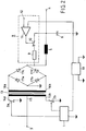
- Fig. 2 shows a transformer-coupled clocked power supply with push-pull circuit and electrical isolation of input and output.
- the middle connection 15 of the symmetrical primary winding of the transformer 13 is connected to the DC voltage input 3
- the outer connections 14a, 14b of the primary winding are alternately connected to the zero point of the primary circuit via electronic switches 2a and 2b.
- a pulse width modulator 1 controls the closing times of the switches 2a , 2b as a function of the voltage at output 4 or as a function of a voltage proportional to the output voltage.
- an arrangement consisting of the secondary winding with connections 16a, 16b and diodes 17a, 17b, 17c and 17d forms a full-wave rectifier, the output of which is connected to the input of a low-pass filter, which consists of inductor 5 and capacitor 6. This filter then forms the mean value of the pulse-width-modulated voltage at the output of the rectifier.
- the feedback of pulse-width modulator 1 to output 4 is via potential-isolating transmission means 18, e.g. an isolation amplifier.
- the supply device again has an impedance, in the simplest case a resistor 9, and a switch 10, which is actuated by a comparator 11 and bridges the inductance 5, the comparator 11 again providing the output voltage with a reference voltage applied to its reference input 12 compares.
- the capacitance 6 is again charged via the bypass circuit 8 until the output voltage has reached the minimum value. In normal operation, the bypass circuit 8 does not conduct.
- the switch 10 in the bypass circuit 8 is advantageous to design as a switchable constant current source, since in this way the current can be optimally dimensioned largely independently of the voltage drop across the bypass circuit.
- Fig. 3 shows an embodiment of the bypass circuit 8 for positive voltage polarity with a switchable constant current source and the low-pass filter in front of the output 4 of a DC-DC converter according to the invention with the bridged inductor 5 and the capacitance 6.
- the known constant current source is a transistor 19, an emitter resistor 20, a Zener diode 21 and a base-collector resistor 22 are formed.
- the zener diode voltage and the emitter resistor 20 determine the value of the current.
- the emitter output of the current source is connected to the output of the filter via a diode 23.
- the diode 23 prevents polarity reversal of the current source during the time intervals when the output voltage of the rectifier is zero due to pulse width modulation and the voltage at output 4 has a positive value.
- the comparator 11 contains a second transistor 24 and a voltage divider 25 between the output voltage and ground, which drives the same, the collector of the transistor 24 being connected to the base of the transistor 19 and its emitter being grounded via a zener diode 26.
- FIG. 4 shows a clocked power supply unit, the basic structure of which corresponds to that of the power supply unit explained in connection with FIG. 2, if one disregards that the transformer 13 still has a central connection 27, which simplifies the construction of the full-wave rectifier with only two Diodes 17a, 17b allowed.
- the secondary winding of the transformer 13 has two further connections 28a, 28b, each branching off, preferably symmetrically to one another, between the central connection 18 and one of the outer connections 16a or 16b, while the bypass circuit 8 consists of two diodes 29a, 29b, over each of which one of the connections 28a, 28b is connected to the output 4.
- the bypass circuit 8 consists of two diodes 29a, 29b, over each of which one of the connections 28a, 28b is connected to the output 4.
- the voltage supplied by the latter, rectified by the diodes 17a, 17b and smoothed by the inductor 5, is therefore higher than the voltage supplied by the connections 28a, 28b and rectified by the diodes 29a, 29b and block the latter.
- an input voltage is applied to the voltage-free supply device, a high voltage drop initially arises via the inductor 5 due to the braking effect of the current increase, and the capacitance 6 is quickly charged via the diodes 29a, 29b.
- a Secondary auxiliary winding 30 has a central connection 31, which is connected to the zero potential of the primary circuit, and two outer connections 32a, 32b, which are connected to the input of a low-pass filter via diodes 33a, 33b, which form a full-wave rectifier.
- the low-pass filter consists of an inductor 34 and a capacitor 35, to which a resistor 36 is placed in parallel.
- This version is particularly recommended as particularly simple, reliable and inexpensive if the value of the input voltage at the time of switching on is exactly known and a significant increase above this value in operation does not have to be expected.
- the devices for feedback with galvanic isolation shown in connection with FIG. 2 and FIG. 4 can of course also be combined with the other embodiment of the invention or, if necessary, completely omitted and the output 4, as in the embodiment according to FIG. 1, directly or via an impedance can be connected to the pulse width modulator 1.
Landscapes
- Engineering & Computer Science (AREA)
- Power Engineering (AREA)
- Dc-Dc Converters (AREA)
Applications Claiming Priority (2)
| Application Number | Priority Date | Filing Date | Title |
|---|---|---|---|
| CH1088/83 | 1983-02-28 | ||
| CH108883 | 1983-02-28 |
Publications (2)
| Publication Number | Publication Date |
|---|---|
| EP0118054A1 true EP0118054A1 (fr) | 1984-09-12 |
| EP0118054B1 EP0118054B1 (fr) | 1986-04-30 |
Family
ID=4202182
Family Applications (1)
| Application Number | Title | Priority Date | Filing Date |
|---|---|---|---|
| EP84101323A Expired EP0118054B1 (fr) | 1983-02-28 | 1984-02-09 | Dispositif d'alimentation à commutation avec entrée en tension continue |
Country Status (3)
| Country | Link |
|---|---|
| US (1) | US4628430A (fr) |
| EP (1) | EP0118054B1 (fr) |
| DE (1) | DE3460110D1 (fr) |
Cited By (4)
| Publication number | Priority date | Publication date | Assignee | Title |
|---|---|---|---|---|
| DE4034605A1 (de) * | 1990-10-31 | 1992-05-07 | Basf Ag | Waessrige dispersionen polymerer pigmente mit hoher lichtstreukraft |
| CN1320751C (zh) * | 2002-11-14 | 2007-06-06 | 国际整流器公司 | 为脉宽调制器集成电路提供抵抗单粒子翻转能力的电路 |
| RU2369895C1 (ru) * | 2008-02-15 | 2009-10-10 | Открытое акционерное общество "Научно-производственный центр "Полюс" | Способ управления преобразователем напряжения |
| AT510804A1 (de) * | 2010-12-07 | 2012-06-15 | Fachhochschule Technikum Wien | Verfahren und vorrichtung zur verbesserung der dynamik von konvertern |
Families Citing this family (6)
| Publication number | Priority date | Publication date | Assignee | Title |
|---|---|---|---|---|
| US5119284A (en) * | 1990-04-05 | 1992-06-02 | General Electric Company | Efficient power supply post regulation |
| US5075839A (en) * | 1990-04-05 | 1991-12-24 | General Electric Company | Inductor shunt, output voltage regulation system for a power supply |
| US5892666A (en) * | 1998-03-31 | 1999-04-06 | Gucyski; Jeff | Push-pull switching power supply having increased efficiency and incorporating power factor correction |
| DE102004060359A1 (de) * | 2004-12-15 | 2006-07-06 | Austriamicrosystems Ag | Laderegleranordnung und Verfahren zum Aufladen einer Batterie |
| US8456267B2 (en) * | 2010-05-14 | 2013-06-04 | Agilent Technologies, Inc. | High-impedance DC-isolating transmission line transformers |
| TWI828036B (zh) * | 2022-01-12 | 2024-01-01 | 光寶科技股份有限公司 | 電子裝置、保護電路及應用其之保護方法 |
Citations (2)
| Publication number | Priority date | Publication date | Assignee | Title |
|---|---|---|---|---|
| DE2817204A1 (de) * | 1978-04-20 | 1979-10-31 | Standard Elektrik Lorenz Ag | Sperrwandler-netzteil |
| GB1594400A (en) * | 1978-05-31 | 1981-07-30 | Coutant Electronics Ltd | Symmetry control system for a converter |
Family Cites Families (8)
| Publication number | Priority date | Publication date | Assignee | Title |
|---|---|---|---|---|
| US1878101A (en) * | 1927-04-29 | 1932-09-20 | Fansteel Prod Co Inc | Rectifier circuit |
| GB1041268A (en) * | 1963-08-02 | 1966-09-01 | Ass Elect Ind | Improvements in or relating to rectifier circuits |
| US3308311A (en) * | 1964-01-21 | 1967-03-07 | Collins Radio Co | Transient suppression circuit |
| SU435511A1 (ru) * | 1972-11-21 | 1974-07-05 | О. А. Жученко , В. П. Горобченко | Импульсный стабилизатор постоянного напряжения |
| US3890557A (en) * | 1973-11-13 | 1975-06-17 | Georgy Yakovlevich Bogdanov | Device for setting up arc current in pulsed arc welding |
| SU691816A1 (ru) * | 1977-06-10 | 1979-10-15 | Московский Ордена Трудового Красного Знамени Электротехнический Институт Связи | Импульсный стабилизатор посто нного напр жени |
| SU781792A2 (ru) * | 1979-02-07 | 1980-11-23 | Предприятие П/Я А-7160 | Источник питани посто нного напр жени |
| US4488200A (en) * | 1982-09-23 | 1984-12-11 | Tokyo Shibaura Denki Kabushiki Kaisha | No-break power supply apparatus |
-
1984
- 1984-02-09 DE DE8484101323T patent/DE3460110D1/de not_active Expired
- 1984-02-09 EP EP84101323A patent/EP0118054B1/fr not_active Expired
- 1984-02-22 US US06/582,484 patent/US4628430A/en not_active Expired - Fee Related
Patent Citations (2)
| Publication number | Priority date | Publication date | Assignee | Title |
|---|---|---|---|---|
| DE2817204A1 (de) * | 1978-04-20 | 1979-10-31 | Standard Elektrik Lorenz Ag | Sperrwandler-netzteil |
| GB1594400A (en) * | 1978-05-31 | 1981-07-30 | Coutant Electronics Ltd | Symmetry control system for a converter |
Non-Patent Citations (1)
| Title |
|---|
| PATENTS ABSTRACTS OF JAPAN; Band 6, Nr. 155, 17. August 1982, Seite 159E125 & JP-A-57 078365 (HITACHI SEISAKUSHO K.K.) 17.05.1982 * |
Cited By (5)
| Publication number | Priority date | Publication date | Assignee | Title |
|---|---|---|---|---|
| DE4034605A1 (de) * | 1990-10-31 | 1992-05-07 | Basf Ag | Waessrige dispersionen polymerer pigmente mit hoher lichtstreukraft |
| CN1320751C (zh) * | 2002-11-14 | 2007-06-06 | 国际整流器公司 | 为脉宽调制器集成电路提供抵抗单粒子翻转能力的电路 |
| RU2369895C1 (ru) * | 2008-02-15 | 2009-10-10 | Открытое акционерное общество "Научно-производственный центр "Полюс" | Способ управления преобразователем напряжения |
| AT510804A1 (de) * | 2010-12-07 | 2012-06-15 | Fachhochschule Technikum Wien | Verfahren und vorrichtung zur verbesserung der dynamik von konvertern |
| AT510804B1 (de) * | 2010-12-07 | 2015-08-15 | Fachhochschule Technikum Wien | Hochdynamischer Konverter |
Also Published As
| Publication number | Publication date |
|---|---|
| DE3460110D1 (en) | 1986-06-05 |
| EP0118054B1 (fr) | 1986-04-30 |
| US4628430A (en) | 1986-12-09 |
Similar Documents
| Publication | Publication Date | Title |
|---|---|---|
| EP1788696B1 (fr) | Circuit de régulation pour la régulation du courant et de la tension dans un circuit d'alimentation de puissance à découpage | |
| EP0309892B1 (fr) | Alimentation de puissance à découpage | |
| DE2832595C2 (fr) | ||
| DE69506096T2 (de) | Sperrwandler | |
| DE3509714A1 (de) | Mitkopplungsschaltung und verfahren zum bilden derselben | |
| DE3886585T2 (de) | Gesteuerte Hochfrequenzleistungsversorgung. | |
| DE69020709T2 (de) | Steuerung mit gemischter Regelungsform für einen resonanten Leistungswandler. | |
| DE102007029388A1 (de) | Eigenstromversorgung für Stromrichterschaltertreiber | |
| EP0241976A1 (fr) | Circuit pour générer une tension continue à partir d'une tension d'entrée sinusoidale | |
| WO1988008638A1 (fr) | Regulateur secondaire combine | |
| DE112017005404T5 (de) | DC-DC Wandler | |
| DE68906857T2 (de) | Doppelkommutierungsleistungssperrwandler. | |
| EP0991171A2 (fr) | Convertisseur à récupération | |
| EP0118054B1 (fr) | Dispositif d'alimentation à commutation avec entrée en tension continue | |
| EP0205630B1 (fr) | Régulateur de découpage et son application | |
| DE10249802A1 (de) | Gleichspannungswandler und Verfahren zur Gleichspannungswandlung | |
| WO1991015048A2 (fr) | Dispositif d'alimentation ininterrompue en courant electrique | |
| DE3026147C2 (de) | Geregelter fremdgetakteter Gleichspannungswandler | |
| DE4008652A1 (de) | Netzteil mit gleichstrom-gleichstrom-wandler | |
| DE60025635T2 (de) | Begrenzung des kontinuierlichen Modes eines Leistungswandlers | |
| DE69628058T2 (de) | Schaltnetzteil | |
| DE69301814T2 (de) | Steuereinrichtung für die Spannungbegrenzung einer Kapazität zur Kern-Rückmagnetisierung | |
| EP0130411B1 (fr) | Dispositif d'alimentation à découpage électronique | |
| DE3238127A1 (de) | Anordnung zur steuerung von halbleiterschaltungen | |
| DE3323371C2 (fr) |
Legal Events
| Date | Code | Title | Description |
|---|---|---|---|
| PUAI | Public reference made under article 153(3) epc to a published international application that has entered the european phase |
Free format text: ORIGINAL CODE: 0009012 |
|
| AK | Designated contracting states |
Designated state(s): CH DE FR LI SE |
|
| 17P | Request for examination filed |
Effective date: 19840712 |
|
| GRAA | (expected) grant |
Free format text: ORIGINAL CODE: 0009210 |
|
| AK | Designated contracting states |
Kind code of ref document: B1 Designated state(s): CH DE FR LI SE |
|
| REF | Corresponds to: |
Ref document number: 3460110 Country of ref document: DE Date of ref document: 19860605 |
|
| ET | Fr: translation filed | ||
| PLBE | No opposition filed within time limit |
Free format text: ORIGINAL CODE: 0009261 |
|
| STAA | Information on the status of an ep patent application or granted ep patent |
Free format text: STATUS: NO OPPOSITION FILED WITHIN TIME LIMIT |
|
| 26N | No opposition filed | ||
| PGFP | Annual fee paid to national office [announced via postgrant information from national office to epo] |
Ref country code: DE Payment date: 19900426 Year of fee payment: 7 |
|
| PGFP | Annual fee paid to national office [announced via postgrant information from national office to epo] |
Ref country code: CH Payment date: 19900518 Year of fee payment: 7 |
|
| PGFP | Annual fee paid to national office [announced via postgrant information from national office to epo] |
Ref country code: FR Payment date: 19910116 Year of fee payment: 8 |
|
| PGFP | Annual fee paid to national office [announced via postgrant information from national office to epo] |
Ref country code: SE Payment date: 19910128 Year of fee payment: 8 |
|
| PG25 | Lapsed in a contracting state [announced via postgrant information from national office to epo] |
Ref country code: LI Effective date: 19910228 Ref country code: CH Effective date: 19910228 |
|
| REG | Reference to a national code |
Ref country code: CH Ref legal event code: PL |
|
| PG25 | Lapsed in a contracting state [announced via postgrant information from national office to epo] |
Ref country code: SE Effective date: 19920210 |
|
| PG25 | Lapsed in a contracting state [announced via postgrant information from national office to epo] |
Ref country code: DE Effective date: 19920701 |
|
| PG25 | Lapsed in a contracting state [announced via postgrant information from national office to epo] |
Ref country code: FR Effective date: 19921030 |
|
| REG | Reference to a national code |
Ref country code: FR Ref legal event code: ST |
|
| EUG | Se: european patent has lapsed |
Ref document number: 84101323.8 Effective date: 19920904 |