EP0118670A2 - Prioritätssystem für Kanalsubsystem - Google Patents
Prioritätssystem für Kanalsubsystem Download PDFInfo
- Publication number
- EP0118670A2 EP0118670A2 EP84100448A EP84100448A EP0118670A2 EP 0118670 A2 EP0118670 A2 EP 0118670A2 EP 84100448 A EP84100448 A EP 84100448A EP 84100448 A EP84100448 A EP 84100448A EP 0118670 A2 EP0118670 A2 EP 0118670A2
- Authority
- EP
- European Patent Office
- Prior art keywords
- priority
- requester
- sequence
- requesters
- cycle
- Prior art date
- Legal status (The legal status is an assumption and is not a legal conclusion. Google has not performed a legal analysis and makes no representation as to the accuracy of the status listed.)
- Granted
Links
Images

Classifications
-
- G—PHYSICS
- G06—COMPUTING OR CALCULATING; COUNTING
- G06F—ELECTRIC DIGITAL DATA PROCESSING
- G06F13/00—Interconnection of, or transfer of information or other signals between, memories, input/output devices or central processing units
- G06F13/14—Handling requests for interconnection or transfer
- G06F13/20—Handling requests for interconnection or transfer for access to input/output bus
-
- G—PHYSICS
- G06—COMPUTING OR CALCULATING; COUNTING
- G06F—ELECTRIC DIGITAL DATA PROCESSING
- G06F13/00—Interconnection of, or transfer of information or other signals between, memories, input/output devices or central processing units
- G06F13/14—Handling requests for interconnection or transfer
- G06F13/16—Handling requests for interconnection or transfer for access to memory bus
- G06F13/18—Handling requests for interconnection or transfer for access to memory bus based on priority control
Definitions
- This invention relates to a priority system for use in the channel subsystem of a data processing system providing a selectable relative priority between secondary data stagers and an I/O processor for access to the system resources, including logic circuits and lines for granting an operating cycle to a requester on the basis of one of a plurality of priority sequences among the requesters, stepping means for stepping the circuit means through the cycle of priority sequences, and means for changing the stepping sequence.
- a system resource such as main memory
- several users such as channels
- Apparatus that resolves this contention can be called a priority circuit.
- a channel subsystem is a conventional part of a data processing system and is well known, it will be helpful to review the features and the terminology of a system that particularly illustrates an application for this invention.
- a single computing engine might issue orders to a disk controller to transfer data and a program into processor store, and the same engine might then execute the program on the data in main store.
- processors there are commonly two separate engines, one for the I/O operations and one for the arithmetic and logic operations for executing a program in main memory.
- I/O processor IOP
- processors that are called channel processors or CP's.
- the central processor handles the I/O operations that directly relate to a users program and the IOP and the CP's handle the operations of transferring data between the I/O devices and the memory of the central processor.
- the CP's handle the actual transfers into and out of processor memory, including the operations with the device controllers.
- the IOP handles general parts of the I/O operation such as communicating with the central processor, scheduling the I/O jobs, and handling the ending status of the CP's.
- the IOP communicates with the central processor for operations such as getting control blocks that the central processor prepares to begin I/O operations and for reporting status conditions that are handled by the central processor instead of by the IOP.
- the CP's communicate with the central processor storage for storing data from an I/O device and for fetching data that is to be stored on an I/O device or for fetching channel programs that are executed by the CP's.
- the IOP and the CP's also communicate with each other.
- the IOP signals a particular CP when an I/O job is to be performed and the CP signals the IOP when the job has been completed or when some other general operation is to be performed by the IOP.
- These communications are commonly carried out over signal wires that run between the IOP and the CP's or by the processor storage.
- I/O subsystem can be simplified by introducing terminology from a specific system that would use the priority circuit of this invention.
- a large number of CP's communicate with processor memory through a system of buffer memories that are arranged in an upwardly pointing funnel shape with a succession of stages in which there are fewer busses than in the stage below but the busses are either wider or faster.
- the secondary data stager has two similar component groups each called a secondary data stager or SDS.
- the IOP and the two SDS's connect to processor memory and to each other through the uppermost stage which is called the primary data stager or PDS.
- PDS primary data stager
- contention between the CP's and the IOP for access to main memory can be described in terms of contention between just the IOP and the two SDS's.
- the PDS provides the communications path between the IOP and the two SDS's, and these components also contend for access to these interconnecting data paths.
- a priority circuit is required because some of the operations of the CP's have critical timing.
- the object of this invention is to provide a new priority system in which a critical CP operation is unlikely to be delayed because a less critical operation of the IOP-is taking place and to prevent a large number of CP's from being delayed because one CP is blocking the IOP from adequate access to main memory.
- a more specific object of this invention is to provide a system that permits an IOP and an SDS (or 2 SDS's) to be given a relative priority on a selectable basis. The object is achieved particularly by the characterizing part of claim 1.
- This invention provides a priority circuit that permits a selectable relative priority between the SDS's and the IOP for access to the system resources.
- An SDS or the IOP signals a request for a particular resource.
- Each resource conventionally provides a busy/available signal.
- the requests for particular resources are matched with the availability of these resources, and requests are signalled only for the contenders for resources that are available.
- access is granted to the requester having the highest priority.
- the sequence of priority for the three contenders is changed in a cycle that contains a variable number of steps.
- the lowest priority contender, the IOP is given highest priority in one of the steps, and top priority alternates between the two SDS's on the other cycles.
- the number of steps is a relatively low priority and in shorter cycles the IOP receives relatively higher priority or achieves substantially equal priority with the SDS's.
- a counter is arranged to count through a full cycle of seven steps or through a smaller number of steps. Each step has a particular sequence of priority.
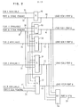
- Fig. 1 shows a central processor complex that includes a central processor, a processor memory, and a circuit that controls access to the memory by the processor and by the I/O subsystem.
- the invention is useful with a wide variety of data processing systems, and in Fig. 1 these components are represented by a functional block 12.
- the IOP and SDSl and SDS2 which have been described earlier are also represented by functional blocks.
- a primary data stager PDS is connected to the memory controller by a bidirectional data bus 14 and by an address and control bus 15.
- a data buffer 16 and a data register 17 are connected in the path of the data bus 14 for input to the processor and data registers 17 and 18 are connected in the path for output from the processor.
- Store request registers SCR1 and SCR2 and fetch request registers FCRl and FCR2 are connected in the path of address and control bus 15 to the processsor.
- Data is transferred on memory bus 14 on successive cycles of the system operations (unless there is no pending transfer).
- data from register 17 are placed on bus 14 and the associated address and control information from register SCRl or SCR2 are placed on bus 15.
- addresses and other information from FCR1 or FCR2 are placed on bus 15 and subsequently data is transferred on memory bus 14 to register 17.
- the priority circuit controls access by the IOP and the SDS's to SCR 1 and 2 and FCR 1 and 2 and the other components operate according to the contents of these registers without regard to priority.
- the IOP and each-SDS are connected to the PDS by separate input busses 20, 21 and 22 and output busses 23, 24, and 25.
- the three input busses are combined in a circuit 27 and the three output busses are split from a circuit 28. These circuits are conventional and do not require specific description.
- the Channel Communicator Array CCA of the application of Blount et al. provides communications between the IOP and the SDS's.
- the priority circuit of this invention controls access to the data input register CCIR of the CCA.
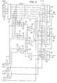
- Fig. 2 shows a port of the PDS that receives one or more requests by SDS1 and matches these requests with the system resources that are available.
- the PDS has two other ports for SDS2 and the IOP that.are identical to the port of Fig. 2 except for differences in their input and output connections.
- Port 0 receives signals on lines 30, 31, and 32 that identify requests by SDS 1 for access to the system resources: Fetch Request Pending, Store Request Pending, and CCA Operation Pending. It receives corresponding signals on lines 33 to 37 that tell whether the system resources are available or busy: SCR1 Available, SCR2 Available, FCRl Available, FCR2 Available, and CCA Input Register (CCIR) Available.
- the other ports receive corresponding request signals and receive the same availability signals.
- the port produces one output signal on a line 39 that indicates that a request has been made and has been matched, and it produces a control signal on one of lines 40 to 44 for identifying the resource for which a request has been matched.
- the request and availability matching function that has just been described is implemented in the circuit of Fig. 2 by a system of AND logic gates 48-52.
- the gates are arranged in a column in the drawing to illustrate a hierarchy for accepting a request in case signal and the corresponding availability signal. This arrangement is illustrated by gate 48 which receives the signals Port 0 Store Pending and SCR1 Available on lines 30 and 33. On the coincidence of these signals, gate 48 produces an output signal Load SCRl Port 0 on line 40.
- Each other gate 49-52 similarly receives a request signal and the corresponding availability signal.
- the output 40-43 of each gate except the last gate 52 is connected to inhibit the output of each gate below it in the column. (Circles in the drawing represent a logic invert function which causes a 1 logic value at an output of a control line 40-44 to appear as a 0 logic value at an input for an inhibiting function in an AND gate.)
- Lines 30-32 from SDS1 are physically distinct conductors that each carry an individual request signal, and it is possible for SDS1 to have simultaneously pending requests for any of the resources.
- the PDS and the priority circuit of Fig. 3 handle only one request on each cycle.
- the inhibit connection from the output of an AND gate to the inputs of the lower gates permits pending requests from the SDS to be accepted in a sequence of priority.
- priority alternates between the SCR's and the FCR's so that they have equal priority to the extent that this can be achieved.
- the circuit of Fig. 2 also has an OR circuit 55 that produces a signal Port 0 Request that signifies that the SDS1 has made a request that has been matched by an available resource.
- this signal is a generalized request for an available resource without regard to the specific identification of the resource.
- the circuit of Fig. 3 receives these generalized requests and grants access to the requester with the highest priority for the cycle.
- the circuit of Fig. 3 receives the generalized request on line 39 from port 0 which was described in the preceding section, and it receives corresponding signals on lines 62 and 63 from ports 1 and 2. Requests from the three ports are independent and on any particular request cycle the three request lines 39, 62, 63 can have 1 or 0 values in any combination. Unless there are no requests, the circuit of Fig. 3 produces a signal on one of lines 64, 65, or 66 to grant access to one of the ports to whatever resource has been matched in its circuit of Fig. 2. The circuit of Fig.
- Fig. 3 comprises a combinatorial logic network that resolves requests on a priority basis and a set of control lines 71 and a counter 72 and decoder 73 that step an enabling signal along the lines to control the logic network to produce different priority sequences with each step.
- the circuit of Fig. 3 also receives a two.bit code 69 and the counter includes means responsive to the mode bits to change its counting sequence to thereby change the relative priority of the IOP and SDS 1 and 2.
- the counter operates through a full count of seven steps. On each step the three ports have a particular sequence of priority. The preferred sequence is as follows.
- Count 1 and that Port 1 has made a request but that Port 0 has not made a request.
- the circuit of Fig. 3 operates to grant priority by default to Port 1, as is set out in Table 1.
- the components for all default conditions are similar, and these components will be described as the operation is described for the default from Port 0 to Port 1.
- the components reflect the asymmetry of Table 1 and will be described separately.
- AND gates 74-76 in the circuit for Port 0 are inhibited by the down level of the signal on line 39.
- AND gate 83 responds to its three input signals to produce a grant signal at the output 65 of OR gate 84.
- An Invert circuit 90 inverts the request from Port 0 on line 39 to produce a signal on a line 91, No Request From Port 0.
- Invert circuits 95, 96, OR gates 97, 98 and AND gates 99 and 100 form default signals on lines 104 and 105 for steps in which Port 1 or Port 2 would otherwise have first priority.
- An OR gate 107 receives the signal Default from Port 0 priority from gate 92 and it also receives the corresponding signal Default from Port 2 on line 105 and it produces an output on a line 109 that signifies that either Port 0 or Port 2 (or both) have defaulted.
- OR gates 110 and 111 form corresponding signals that signify that a default has occurred in the combination Ports 1 or 2 or Ports 0 or 1.
- AND gate 77 for Port 0 receives the output of OR gate 110, and a request by Port 0 on line 39 produces a grant signal on line 64 in any case of default from first priority by any other port.
- AND gate 83 for Port 1 receives the default signal from OR gate 107 but it also receives an inhibiting input from OR gate 78 if Port 0 has made a request.
- This combination of signals is logically equivalent to ((Step 1, 3, 5) AND Not (Request by Port 0)) OR (Step 7 AND Not (request by Port 0 OR Port 2)).
- the default priority is port 0, 1, 2.
- AND gate 114 for Port 2 receives the signal for a default from either Port 0 or Port 1 from OR gate 111 and it also receives inhibiting inputs from lines 64 and 65 that signify by an up level after inversion that a request has not been granted to either Port 0 or Port 1.
- This combination of signals is logically equivalent to ((Step 1, 3, or 5) AND NOT (Request by Port 0)) OR ((Step 2, 4 or 6) AND NOT (Request by Port 1)).
- Table 2 shows the counting sequence for counting cycles 3, 4, and 5 steps and also shows the mode control bits for all four counting sequences.
- Port 0 and Port 1 receives first or second priority on two of the three steps. Similarly, in the sequence of mode bits 01, Port 0 and Port 1 receive first or second priority on three of the four steps.
- the relative priority between ports 0 and 1 is made slightly asymmetrical by the single step in which Port 2 has first priority, and in the sequence for mode bits 01 the relative priority is made somewhat more unsymmetrical by the fact that there are an even number of total count steps and an odd number of steps to be divided between ports 0 and 1. This asymmetry will ordinarily not be apparent to a user of the system.
- the preferred counter is a simple series of three interconnected latch stages with controlled interstage coupling that selectively cause the latch to advance from an existing count to a selected next count. For example, when the counter is controlled by mode bits 11, the latch advances from count 100 (decimal 4) to count 101 (decimal 5) by the familiar operation of interstage coupling that flips the rightmost bit and conditionally flips certain adjacent bits. Similarly, in modes 00, 01 or 10, the counter advances from count 100 to count 111 (decimal 7) by flipping to two rightmost bits. Counters for various sequences are well known and will be readily understood from these examples.
- a counter is a sequential circuit, that responds to a stepping signal that is formed from a clock of the I/O subsystem, and it responds also to its existing state to advance to the next counting step in the sequence.
- a stepping signal that is formed from a clock of the I/O subsystem, and it responds also to its existing state to advance to the next counting step in the sequence.
Landscapes
- Engineering & Computer Science (AREA)
- Theoretical Computer Science (AREA)
- Physics & Mathematics (AREA)
- General Engineering & Computer Science (AREA)
- General Physics & Mathematics (AREA)
- Bus Control (AREA)
Applications Claiming Priority (2)
| Application Number | Priority Date | Filing Date | Title |
|---|---|---|---|
| US46595383A | 1983-02-14 | 1983-02-14 | |
| US465953 | 1983-02-14 |
Publications (3)
| Publication Number | Publication Date |
|---|---|
| EP0118670A2 true EP0118670A2 (de) | 1984-09-19 |
| EP0118670A3 EP0118670A3 (en) | 1988-04-20 |
| EP0118670B1 EP0118670B1 (de) | 1991-04-03 |
Family
ID=23849841
Family Applications (1)
| Application Number | Title | Priority Date | Filing Date |
|---|---|---|---|
| EP19840100448 Expired EP0118670B1 (de) | 1983-02-14 | 1984-01-17 | Prioritätssystem für Kanalsubsystem |
Country Status (3)
| Country | Link |
|---|---|
| EP (1) | EP0118670B1 (de) |
| JP (1) | JPS59148952A (de) |
| DE (1) | DE3484357D1 (de) |
Cited By (5)
| Publication number | Priority date | Publication date | Assignee | Title |
|---|---|---|---|---|
| EP0242882A3 (en) * | 1986-04-25 | 1990-01-10 | Hitachi, Ltd. | Storage control method and apparatus |
| EP0463943A3 (de) * | 1990-06-22 | 1992-12-30 | Digital Equipment Corporation | Schneller Arbitrierer mit einfacher Anpassung für eine grosse Anzahl von Anforderern mit grosser Anzahl von mehreren Betriebsmitteltypen und selektierbaren Methoden von Warteschleifen |
| GB2278258A (en) * | 1993-05-17 | 1994-11-23 | Ibm | Token ring network |
| GB2336273A (en) * | 1998-01-30 | 1999-10-13 | Sgs Thomson Microelectronics | Arbitration circuitry |
| GB2337138A (en) * | 1998-01-30 | 1999-11-10 | * Sgs-Thomson Microelectronics Limited | Arbitrating between a plurality of requests to access resources |
Families Citing this family (2)
| Publication number | Priority date | Publication date | Assignee | Title |
|---|---|---|---|---|
| JP2633900B2 (ja) * | 1988-04-22 | 1997-07-23 | 株式会社日立製作所 | 共通バス制御方法 |
| US5311461A (en) * | 1988-12-30 | 1994-05-10 | International Business Machines Corp. | Programmable priority and selective blocking in a compute system |
Family Cites Families (5)
| Publication number | Priority date | Publication date | Assignee | Title |
|---|---|---|---|---|
| US3699530A (en) * | 1970-12-30 | 1972-10-17 | Ibm | Input/output system with dedicated channel buffering |
| US3812473A (en) * | 1972-11-24 | 1974-05-21 | Ibm | Storage system with conflict-free multiple simultaneous access |
| JPS522127A (en) * | 1975-06-24 | 1977-01-08 | Hitachi Ltd | Memory access control circuit |
| US4126897A (en) * | 1977-07-05 | 1978-11-21 | International Business Machines Corporation | Request forwarding system |
| JPS56166559A (en) * | 1980-05-28 | 1981-12-21 | Hitachi Ltd | Precedence selecting device |
-
1983
- 1983-11-18 JP JP58216377A patent/JPS59148952A/ja active Pending
-
1984
- 1984-01-17 DE DE8484100448T patent/DE3484357D1/de not_active Expired - Lifetime
- 1984-01-17 EP EP19840100448 patent/EP0118670B1/de not_active Expired
Cited By (9)
| Publication number | Priority date | Publication date | Assignee | Title |
|---|---|---|---|---|
| EP0242882A3 (en) * | 1986-04-25 | 1990-01-10 | Hitachi, Ltd. | Storage control method and apparatus |
| EP0463943A3 (de) * | 1990-06-22 | 1992-12-30 | Digital Equipment Corporation | Schneller Arbitrierer mit einfacher Anpassung für eine grosse Anzahl von Anforderern mit grosser Anzahl von mehreren Betriebsmitteltypen und selektierbaren Methoden von Warteschleifen |
| US5303391A (en) * | 1990-06-22 | 1994-04-12 | Digital Equipment Corporation | Fast arbiter having easy scaling for large numbers of requesters, large numbers of resource types with multiple instances of each type, and selectable queuing disciplines |
| US5313641A (en) * | 1990-06-22 | 1994-05-17 | Digital Equipment Corporation | Fast arbiter having easy scaling for large numbers of requesters, large numbers of resource types with multiple instances of each type, and selectable queing disciplines |
| GB2278258A (en) * | 1993-05-17 | 1994-11-23 | Ibm | Token ring network |
| GB2336273A (en) * | 1998-01-30 | 1999-10-13 | Sgs Thomson Microelectronics | Arbitration circuitry |
| GB2337138A (en) * | 1998-01-30 | 1999-11-10 | * Sgs-Thomson Microelectronics Limited | Arbitrating between a plurality of requests to access resources |
| GB2337138B (en) * | 1998-01-30 | 2002-12-18 | * Sgs-Thomson Microelectronics Limited | Arbitration |
| GB2336273B (en) * | 1998-01-30 | 2003-05-21 | * Sgs-Thomson Microelectronics Limited | A system for accessing resources |
Also Published As
| Publication number | Publication date |
|---|---|
| DE3484357D1 (de) | 1991-05-08 |
| EP0118670A3 (en) | 1988-04-20 |
| JPS59148952A (ja) | 1984-08-25 |
| EP0118670B1 (de) | 1991-04-03 |
Similar Documents
| Publication | Publication Date | Title |
|---|---|---|
| US4675812A (en) | Priority circuit for channel subsystem having components with diverse and changing requirement for system resources | |
| EP0380857B1 (de) | Arbitrierung von Übertragungsanforderungen in einem Multiprozessor-Rechnersystem | |
| US4195342A (en) | Multi-configurable cache store system | |
| US4636942A (en) | Computer vector multiprocessing control | |
| US5379434A (en) | Apparatus and method for managing interrupts in a multiprocessor system | |
| US4901230A (en) | Computer vector multiprocessing control with multiple access memory and priority conflict resolution method | |
| US3812473A (en) | Storage system with conflict-free multiple simultaneous access | |
| US4633394A (en) | Distributed arbitration for multiple processors | |
| US4481572A (en) | Multiconfigural computers utilizing a time-shared bus | |
| EP0078389B1 (de) | Buskonkurrenzbetriebs-Auflösung in einer Datenverarbeitungsanlage mit mehreren unabhängigen Benutzern | |
| US4661900A (en) | Flexible chaining in vector processor with selective use of vector registers as operand and result registers | |
| US4972313A (en) | Bus access control for a multi-host system using successively decremented arbitration delay periods to allocate bus access among the hosts | |
| EP0550147B1 (de) | Verfahren und Gerät zur Arbitrierung auf Basis der Verfügbarkeit von Betriebsmitteln | |
| US4115854A (en) | Channel bus controller | |
| US3399384A (en) | Variable priority access system | |
| US4542455A (en) | Signal-processing multiprocessor system | |
| US3573856A (en) | Distributed priority of access to a computer unit | |
| JP2501419B2 (ja) | 多重プロセッサメモリシステム及びメモリ参照競合解決方法 | |
| GB2366883A (en) | Data processing apparatus with a bus system | |
| JPS62189549A (ja) | 多重階層レベルマルチプロセツサ装置 | |
| US5371893A (en) | Look-ahead priority arbitration system and method | |
| EP0327203A2 (de) | Nichtblockierender NxM-Arbitrierungsschalter mit grosser Bandbreite | |
| US4604685A (en) | Two stage selection based on time of arrival and predetermined priority in a bus priority resolver | |
| EP0118670B1 (de) | Prioritätssystem für Kanalsubsystem | |
| US4837688A (en) | Multi-channel shared resource processor |
Legal Events
| Date | Code | Title | Description |
|---|---|---|---|
| PUAI | Public reference made under article 153(3) epc to a published international application that has entered the european phase |
Free format text: ORIGINAL CODE: 0009012 |
|
| AK | Designated contracting states |
Designated state(s): DE FR GB |
|
| 17P | Request for examination filed |
Effective date: 19841123 |
|
| PUAL | Search report despatched |
Free format text: ORIGINAL CODE: 0009013 |
|
| AK | Designated contracting states |
Kind code of ref document: A3 Designated state(s): DE FR GB |
|
| 17Q | First examination report despatched |
Effective date: 19890830 |
|
| GRAA | (expected) grant |
Free format text: ORIGINAL CODE: 0009210 |
|
| AK | Designated contracting states |
Kind code of ref document: B1 Designated state(s): DE FR GB |
|
| REF | Corresponds to: |
Ref document number: 3484357 Country of ref document: DE Date of ref document: 19910508 |
|
| ET | Fr: translation filed | ||
| PLBE | No opposition filed within time limit |
Free format text: ORIGINAL CODE: 0009261 |
|
| STAA | Information on the status of an ep patent application or granted ep patent |
Free format text: STATUS: NO OPPOSITION FILED WITHIN TIME LIMIT |
|
| 26N | No opposition filed | ||
| PGFP | Annual fee paid to national office [announced via postgrant information from national office to epo] |
Ref country code: GB Payment date: 19921222 Year of fee payment: 10 |
|
| PGFP | Annual fee paid to national office [announced via postgrant information from national office to epo] |
Ref country code: FR Payment date: 19921223 Year of fee payment: 10 |
|
| PGFP | Annual fee paid to national office [announced via postgrant information from national office to epo] |
Ref country code: DE Payment date: 19930127 Year of fee payment: 10 |
|
| PG25 | Lapsed in a contracting state [announced via postgrant information from national office to epo] |
Ref country code: GB Effective date: 19940117 |
|
| GBPC | Gb: european patent ceased through non-payment of renewal fee |
Effective date: 19940117 |
|
| PG25 | Lapsed in a contracting state [announced via postgrant information from national office to epo] |
Ref country code: FR Effective date: 19940930 |
|
| PG25 | Lapsed in a contracting state [announced via postgrant information from national office to epo] |
Ref country code: DE Effective date: 19941001 |
|
| REG | Reference to a national code |
Ref country code: FR Ref legal event code: ST |