EP0118763A2 - Verfahren zur Fehlerortung in einer digitalen Übertragungsleitung - Google Patents
Verfahren zur Fehlerortung in einer digitalen Übertragungsleitung Download PDFInfo
- Publication number
- EP0118763A2 EP0118763A2 EP84101290A EP84101290A EP0118763A2 EP 0118763 A2 EP0118763 A2 EP 0118763A2 EP 84101290 A EP84101290 A EP 84101290A EP 84101290 A EP84101290 A EP 84101290A EP 0118763 A2 EP0118763 A2 EP 0118763A2
- Authority
- EP
- European Patent Office
- Prior art keywords
- repeater
- error
- signal
- transmission system
- error rate
- Prior art date
- Legal status (The legal status is an assumption and is not a legal conclusion. Google has not performed a legal analysis and makes no representation as to the accuracy of the status listed.)
- Granted
Links
Images


Classifications
-
- H—ELECTRICITY
- H04—ELECTRIC COMMUNICATION TECHNIQUE
- H04L—TRANSMISSION OF DIGITAL INFORMATION, e.g. TELEGRAPHIC COMMUNICATION
- H04L1/00—Arrangements for detecting or preventing errors in the information received
- H04L1/24—Testing correct operation
-
- H—ELECTRICITY
- H04—ELECTRIC COMMUNICATION TECHNIQUE
- H04B—TRANSMISSION
- H04B17/00—Monitoring; Testing
- H04B17/40—Monitoring; Testing of relay systems
Definitions
- This invention relates to a method of searching fault locations in a digital transmission line and more particularly to a searching method such as to permit speedy detection of faulty repeaters in the digital transmission line.
- the fiber optic PCM transmission line is such a system as converts a signal into an optical pulse.
- a semiconductor laser is excited by a PCM signal current to be transmitted thereby to generate the optical pulse.
- This optical pulse is transmitted through the optical transmission line.
- repeaters exist on the way of the transmission line the optical pulse is once converted there into an electrical signal. And this electrical signal is restored to an optical pulse again by the excitation of the semiconductor laser and the thus formed optical pulse is fed to a subsequent repeater section in the transmission line.
- the digital signal delivered from a transmitter in a transmitting terminal is deteriorated on the way of a transmission line, but the deteriorated signal is amplified by a repeater and the amplified signal is fed to a subsequent repeater section.
- this function of repeating is accompanied by any fault, it is necessary to remotely search the repeater with which the fault occurs, at the transmitting terminal or a receiving terminal.
- the transmitted signal is subjected to a line coding with error detection capability, and the thus detected error is transmitted to the transmitting terminal or the receiving terminal through a fault signal transmitter, using a twisted pair cable.
- the transmitting terminal or receiving terminal totalizes the error detected at each repeating point (repeater) and calculates the error rate difference between adjoining repeating points to obtain the error rate at each repeater section, thereby determining the repeater section where the fault occurs.
- the error information produced from each repeating point is reported by a signal having specific frequency or address for respective repeater sections, which allows the receiving terminal or transmitting terminal to discriminate the repeating point, from which the error information is transmitted.
- This method requires calculating of the error rate difference between the adjoining repeating points, and hence in order to estimate the repeating point where the maximum error rate occurs, it is necessary to measure the error rate at every repeater and calculate every error rate difference. This method requiring more time and labor is not practical.
- An object of this invention is to overcome the problem in the conventional method mentioned above and to provide a method of searching fault locations in a digital transmission line which can reduce search time and labor by easy detection of the fault locations.
- a method of searching fault locations which is employed in a transmission system comprising a transmitting terminal having a transmitter for transmitting a digital signal; a receiving terminal having a receiver for receiving the digital signal; a plurality of repeaters which are placed between the transmitting and receiving terminals, and each of which receives and amplifies the digital signal from a preceding repeater section and delivers it to a subsequent repeater section; and a plurality of transmission lines for connecting the transmitter with the first repeater, the intermediate repeaters with each other and the final repeater with the receiver, respectively; and which comprises the steps of coding an original signal to be transmitted in terms of two kinds of error detecting codes at the transmitting terminal to send out them from the transmitter; detecting an error of a received signal using one of the two kinds of error detecting codes at each repeater thereby to measure the error rate occurred at one repeater section corresponding to each repeater; recoding a decoded received signal using the error detecting code employed to detect the error, and delivering the recoded signal to the subsequent
- two kinds of error detecting codes are combined to be used, and one of the error detecting codes is recoded, which permits the error rate at one repeater section corresponding to each repeater to be discretely measured and the receiving terminal to count the overall error rate of the transmission line.
- the fault location can be swiftly detected from the error rate at each repeater, which results in the substantial reduction of time and cost taken to search the fault locations.
- Fig. 1 The coding process of a transmission signal in accordance with this invention is illustrated in Fig. 1, and the digital transmission system in which this invention is used is illustrated in Fig. 2.
- the transmission system of Fig. 2 includes a transmitting terminal 1 having a transmitter 2 for transmitting a digital signal; a receiving terminal 5 having a receiver 8 for receiving the digital signal; a plurality of repeaters 4, 4, ... which are placed between the transmitting and receiving terminals, and each of which receives and amplifies the digital signal from a preceding repeater section and delivers it to a subsequent repeater section; and a plurality of transmission lines 3, 3, ... for connecting the transmitter 2 with the first repeater 4, the repeaters with each other and the final repeater 4 with the receiver 8, respectively.
- a fault signal transmitter 6 provided for each repeater (repeating point) serves to transmit error information to a fault signal receiver 10 in the receiving terminal 5 or a fault signal receiver 9 in the transmitting terminal 1 through a fault signal transmission cable 7.
- the cable 7 is usually twisted around the transmission lines 3, 3 ....
- the repeater functions to perform an AMI (Alternate Mark Inversion) recoding for the received signal to deliver it to a subsequent repeater section.
- AMI Alternate Mark Inversion
- Fig.-l(a) shows an original code. This code is parity-coded in the transmitting terminal 1 so that it may be error-detectable, as shown in Fig. l(b).
- One block includes 6 bits - the correspondences are shown by arows - and a parity pulse is inserted into a part indicated by oblique lines so that the number of pulses in a block may be odd (odd parity).
- Fig. l(b) shows two blocks in which a parity pulse is not inserted in the first block since three pulses exist therein while a parity pulse (indicated by oblique lines) is inserted in the second block since two (even) pulses exist therein.
- AMI coding is applied to the parity-coded signal so that AMI coded signal is obtained as shown in Fig. l(c).
- the transmitter 2 transmits the AMI coded signal to a transmission line.
- the low frequency signal component of the signal is cut off by a transformer or capacitor in transmission line 3; hence the code shown in Fig. l(b) gives rise to DC variations in a reshaped pulse train as well as drifts depending on the mark ratio of pulse train and these make the discrimination and regeneration thereof difficult.
- the AMI code bipolar code
- the porality of which code is inverted for each pulse from positive to negative or vice versa is used, the spectrum of which is of the maximum energy near one-half of the pulse repetition frequency.
- the error rate over the entire transmission line can be detected through parity- check, after decoding the AMI signal, as seen from Fig. l(f), at the receiving terminal 5. This may be always supervised by the receiver 8.
- the errors at the repeater section are detected and counted at each repeater (repeating point).
- a fault signal is transmitted from the fault signal transmitter 6.
- the fault signal receiver 9 or 10 it is possible to estimate the repeater section where the fault occurs, by receiving the fault signal at the fault signal receiver 9 or 10.
- the fault signal can be discriminated by allocating addresses.
- Figs. 3 to 11 are diagrams showing the embodiments of respective elements or parts of Figs. 1 and 2.
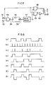
- Figs. 3 and 4 are a block diagram of a parity coder used to execute this invention and a time chart for explaining the operation thereof, respectively.
- the code of Fig. l(a) is coded into an odd number parity code of Fig. l(b) by the parity coder of Fig. 3.
- An original signal such as shown in Fig. 4(a) is supplied from an input terminal 21, phase-adjusted by a delay circuit 22 and applied to a logical product (AND) gate 23.
- this gate 23 is supplied with a clock pulse b such as shown in Fig. 4(b).
- a waveform c such as shown in Fig. 4(c) appears at an output terminal 25.
- Clock pulse b is suppressed for one time slot at the end of respective blocks so that a parity pulse may be inserted there.
- the output waveform c from the gate 23 is directly applied to a logical sum (OR) gate 30 and at the same time applied to a trigger type flip-flop 26.
- the trigger type flip-flop 26 is reset each time a parity clock e such as shown in Fig. 4(e) is applied from a terminal 27.
- the trigger type flip-flop repeats set/reset operation each time a pulse appears in the pulse train c shown in Fig. 4(c), and is reset by the parity clock e, with the result that a waveform d such as shown in Fig. 4(d) is obtained.
- a logical product between the inversion of the waveform d, a waveform 5 and the parity clock e is obtained by a gate 28, and a parity pulse f appears at an output terminal 29.
- a pulse train g such as shown in Fig. 4(g) at the output terminal thereof.
- This pulse train is applied to a pulse expanding circuit 31, with the result that an NRZ (Non Return to Zero) pattern h added with parities is obtained at an output terminal 32.
- the NRZ pattern of Fig. 4(h) is a code added with parities shown in Fig. l(b). Thus, the odd parity code is formed.
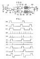
- Figs. 5 and 6 are a block diagram of an AMI coding circuit used for implementing this invention and a time chart for explaining the operation thereof, respectively.
- the NRZ pulse train a added with parities which is obtained by the circuit of Fig. 3 is applied to an input terminal 51 of the AMI coding circuit of Fig. 5 while a clock pulse b such as shown in Fig. 6(b) is applied to a terminal 52 thereof.
- a clock pulse b such as shown in Fig. 6(b)
- the logical product between the pulse train a and the clock pulse b is obtained in the gate 53 and such a waveform c as shown in Fig. 6(c) appears as an output 54.
- This waveform c is applied to a trigger type flip-flop 55, and then such a waveform d as shown in Fig. 6(d) appears as an output 56.
- the waveform e obtained by delaying the output 56 in a delay circuit 57 is applied to a logical product gate 59 while the inverted waveform thereof is applied to a logical product gate 58.
- Both logical product gates 58 and 59 are supplied with the input signal a.
- the logical product gate 59 takes a logical product between the input signal a and the delayed waveform e to obtain a waveform g as an output.
- the logical product gate 58 takes a logical product between the input signal a and an inversion waveform of the delayed waveform e to obtain a waveform f as an output.
- An adder 61 adds the waveform f and an inversion waveform of the waveform g obtained by an inverter 60 thereby to obtain an AMI code the polarity of which is inverted for every pulse, at an output terminal 62.
- AMI code shown in Fig. l(c) is transmitted from the transmitter 2 of the transmitting terminal 1 to the transmission line 3.
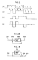
- Figs. 7 and 8 are a block diagram of an error detecting circuit used to implement this invention and a time chart for explaining the operation thereof, respectively.
- the AMI signal When the AMI signal is applied to an input terminal 71 in the error detecting circuit, it is rectified to a positive polarity part and a negative polarity part by half-wave rectification circuits 72 and 73, respectively. And rectified waveforms b and c such as shown in Figs. 8(b) and 8(c) appear at outputs 74 and 75. These waveforms b and c are applied to leading-edge detecting circuits 76 and 77 to take out pulse trains d and e respectively representing the leading edges of the waveforms b and c, as outputs 78 and 79 (Figs: 8(d) and 8(e)).
- the pulse trains d and e are applied to logical product gates 85 and 86, respectively, and simultaneously applied to input terminals 80 and 81 of a set-reset type flip-flop 82, respectively.
- the flip-flop 82 is set each time the pulse of Fig. 8(d) is inputted, while it is reset each time the pulse of Fig. 8(e) is inputted.
- a waveform f such as shown in Fig. 8(f) appears at an output 83 while an inversion waveform of the waveform f appears at an output 84.
- a logical product gate 85 takes a logical product between the pulse train d and the waveform f while a logical product gate 86 takes a logical product between the pulse train e and the inverted waveform of the waveform f.
- a logical sum gate 89 takes a logical sum between the outputs from the gates 85 and 86 thereby to obtain an error pulse g.
- Taking a logical product between the pulses of Figs. 8(d) and 8(f) provides no output at an output 87 since the pulse d is not included in the positive polarity period of the waveform f.
- taking a logical product between the pulse of F ig.
- Fig. 9 illustrates a circuit consisting of an error register and a fault signal transmitter.
- the error pulse g of Fig. 8(g) applied to an input terminal 91 is automatically registered by counters (flip-flops) 93 - 96 through a logical product gate 92.
- the application of the error pulse g to an input terminal 91 sets the flip-flop 93 corresponding a first bit past the gate 92.
- the application of a next error pulse g to the terminal 91 resets the first bit flip-flop 93, and the second bit flip-flop 94 is set.
- the number representing an overflow output i.e., the maximum number of the error pulses to be registered can be optionally determined by increasing the number of the flip-flops.
- the application of the start signal to the input terminal 102 resets all of the flip-flops, and error registration is started again.
- Figs. 10 and 11 are a block diagram of a recoding circuit employed to implement this invention and a time chart for explaining the operation thereof.
- the AMI signal received by the receiver 8 in the receiving terminal 5 is applied to half-wave rectification circuits relative to a positive polarity part and a negative polarity part thereof, respectively, from which rectified waveforms a and b are derived (Figs. 11(a) and 11(b)). Such an operation is the same as that in each repeater, and so these waveforms a and b are equivalent to the waveforms b and c shown in Figs. 8(b) and 8(c).
- the respective application of the rectified waveforms a and b to input terminals 111 and 112 allows a logical sum gate 113 to provide a logical sum output waveform c (Fig. 11(c)).
- the application of this output waveform c to a logical product gate 115 as well as that of a clock d from input terminal 114 provides a sampled waveform e as an output (Fig. 11(e)).
- the application of this sampled waveform e to a trigger type flip-flop 116 gives rise to a waveform f shown in Fig. ll(f) at an output terminal 118.
- a logical product gate 119 takes a logical product between the inversion of the waveform f and the sampled waveform e, which provides a pulse waveform g shown in Fig. ll(g).
- a logical product gate 120 takes a logical product between the waveform f and the sampled waveform e, which provides a pulse waveform h shown in Fig. ll(h).
- the waveform f is slightly delayed by the flip-flop l16 so that it can take a coincidence with the waveform e immediately before the trailing edge of the waveform f while the sampled waveform e occurred immediately before the leading edge of the waveform f can not take a coincidence with the waveform f.
- the time constants of the pulse expanding circuits 123 and 124 are predetermined to be the same time as the period of the clock pulse d.
- An adder 129 addes an inversion of the waveform j obtained through an inverter 127 and the waveform i, which provides a recoded waveform k at an output terminal 128.
- This waveform k corresponding to the waveform e shown in Fig. 1(e) is converted to an NRZ code added with parities shown in Fig. l(f) and thereafter is subjected to parity check.
- the disappearance of pulse indicated by dashed lines in Fig. l(g) can be detected.
- both AMI code and parity code are used has been described hereinbefore. However, it is evident that any kinds of codes can be combined, provided that two kinds of codes are orthogonal with each other, or are not influenced by each other.
- using both parity code and a two-level AMI code in which the two-level AMI code ("1" is converted to "11” or "00” while “0” is converted “10” or “01") sent from the transmitting terminal is duobinary shaped by a roll-off filter at a receiving terminal to obtain the AMI code - allows the fault location searching method according to the present invention to be applied in such a transmission system as optical communications in which the use of two-level code is desirable at the transmitter.
- the above transmission system using a two-level AMI code is described in the article entitled "Optical pulse formats for fiber optic digital communications" in IEEE Trans on Commun. COM-24 No. 4 pp 404 - 413, 1976 April.
- the above two-level code by which "1” is converted into “11” or “00” while “0” is converted into “10” or “01”, is called a DMI (Differential Mark Inversion) code and so is hereinafter referred to as the DMI code.
- DMI coding is performed at a transmitting terminal and the DMI code is converted into the AMI code at a receiving terminal by means of narrow-band shaping.
- the DMI code is also employed for recoding at repeating points.
- the DMI code is not suitable for such a system which uses an optical device such as light emitting diodes (LED). This is because the DMI code requires a double modulating speed as compared with the NRZ code while the optical device such as a light emitting diode finds difficulty in adapting high-modulating speed. In these circumstances, it is necessary to provide a coding system having the modulating speed substantially equal to that of NRZ coding.
- precoding is adapted to the NRZ pulse train at the transmitting terminal, i.e., signals "1" and "0" are converted into a transition and no transition (or vice versa). These converted signals undergo a differentiation shaping at the receiving terminal to obtain an AMI code. This enables the search of fault locations.
- Figs. 12 - 14 The application of an original signal such as shown in Fig. 12(a) to an input terminal 241 of the precoder shown in Fig. 13 gives rise to an output coded as shown in Fig. 12(b) at an output terminal 244.
- This latter signal is such as the result of modulo two addition of the input signal and the output signal by a modulo two adder 242 is delayed by one bit by a delay line 243.
- "1" and "0" of the original signal a shown in Fig. 12(a) correspond to a transition and no transition of the waveform b shown in Fig. 12(b).
- the waveform shown in Fig. 12(b) which is also assumed to be the received waveform is applied to an input terminal 250 of the decoder shown in Fig. 14 and delayed by a delay circuit 251 with the result that a waveform c such as shown in Fig. 12(c) is obtained.
- Subtracting the delayed waveform c from the non-delayed waveform b by a subtracter 252 provides a waveform d such as shown in Fig. 12(d).
- This waveform d is an AMI pulse train in which "1" and "-l" correspond to "1" of the original signal while "0" corresponds to "0" of the original signal.
- the AMI waveform is obtained at the receiving terminal, which allows the search of fault locations according to the method described above. That is, the detection of a violation of the AMI code in each repeater - an AMI code alternately gives "1" and "-1" in a normal state and hence any state other than this state means a violation - permits the fault condition of each repeater section to be searched. This can be carried out in such a manner that the AMI code is once converted to an NRZ code at each repeater, precoded again and transmitted to a subsequent repeater section.
- the search of fault locations can be carried out with the modulating speed substantially equivalent to that in the NRZ code. It is therefore very meritorious to adapt this invention to the transmission system in which the modulating speed is restricted due to the light emitting diodes or the like.
Landscapes
- Engineering & Computer Science (AREA)
- Computer Networks & Wireless Communication (AREA)
- Signal Processing (AREA)
- Physics & Mathematics (AREA)
- Electromagnetism (AREA)
- Dc Digital Transmission (AREA)
Applications Claiming Priority (4)
| Application Number | Priority Date | Filing Date | Title |
|---|---|---|---|
| JP40455/83 | 1983-03-11 | ||
| JP58040455A JPS59167161A (ja) | 1983-03-11 | 1983-03-11 | デイジタル伝送路の障害位置探索方式 |
| JP24693183A JPS60141052A (ja) | 1983-12-28 | 1983-12-28 | デイジタル伝送路における障害位置探索方式 |
| JP246931/83 | 1983-12-28 |
Publications (3)
| Publication Number | Publication Date |
|---|---|
| EP0118763A2 true EP0118763A2 (de) | 1984-09-19 |
| EP0118763A3 EP0118763A3 (en) | 1987-07-22 |
| EP0118763B1 EP0118763B1 (de) | 1990-05-09 |
Family
ID=26379912
Family Applications (1)
| Application Number | Title | Priority Date | Filing Date |
|---|---|---|---|
| EP84101290A Expired - Lifetime EP0118763B1 (de) | 1983-03-11 | 1984-02-08 | Verfahren zur Fehlerortung in einer digitalen Übertragungsleitung |
Country Status (4)
| Country | Link |
|---|---|
| US (1) | US4604745A (de) |
| EP (1) | EP0118763B1 (de) |
| CA (1) | CA1205561A (de) |
| DE (1) | DE3482230D1 (de) |
Cited By (6)
| Publication number | Priority date | Publication date | Assignee | Title |
|---|---|---|---|---|
| AU590489B1 (en) * | 1988-06-01 | 1989-11-02 | Siemens Aktiengesellschaft | Method for supervising the quality of a digital signal in sections of a transmission link |
| AU620526B2 (en) * | 1989-07-10 | 1992-02-20 | Kabushiki Kaisha Toshiba | Redundancy data transmission device |
| EP0474384A3 (en) * | 1990-09-04 | 1993-03-31 | International Business Machines Corporation | Method and apparatus for isolating faults in a network having serially connected links |
| WO1994029983A1 (en) * | 1993-06-10 | 1994-12-22 | Adc Telecommunications, Inc. | Performance monitoring and failure isolation in a point-to-multipoint communication network |
| US8547824B2 (en) | 1994-09-26 | 2013-10-01 | Htc Corporation | Systems and methods for orthogonal frequency divisional multiplexing |
| US11787127B2 (en) | 2019-04-17 | 2023-10-17 | Hutchinson | Method of manufacturing a grille for a thrust reverser |
Families Citing this family (20)
| Publication number | Priority date | Publication date | Assignee | Title |
|---|---|---|---|---|
| JPS6170637A (ja) * | 1984-09-11 | 1986-04-11 | インタ−ナショナル ビジネス マシ−ンズ コ−ポレ−ション | 多数決によるエラ−検出訂正方法 |
| US4710924A (en) * | 1985-09-19 | 1987-12-01 | Gte Sprint Communications Corp. | Local and remote bit error rate monitoring for early warning of fault location of digital transmission system |
| US4713810A (en) * | 1985-09-19 | 1987-12-15 | Gte Sprint Communications Corp. | Diagnostic technique for determining fault locations within a digital transmission system |
| US4756005A (en) * | 1986-05-27 | 1988-07-05 | American Telephone And Telegraph Company At&T Bell Laboratories | Digital signal regenerator arranged for fault location |
| US5317278A (en) * | 1990-07-23 | 1994-05-31 | Rc Concepts, Inc. | Switched active fault locate filter |
| US5555274A (en) * | 1992-03-02 | 1996-09-10 | Teltrend Inc. | Phantom data link for digital transmission lines |
| FR2702910B1 (fr) * | 1993-03-16 | 1995-04-28 | Cit Alcatel | Système pour rétablir la qualité de transmission d'une liaison incluant des équipements amplificateurs, en cas de défaillance d'un ou de plusieurs de ces équipements amplificateurs. |
| USRE42236E1 (en) | 1995-02-06 | 2011-03-22 | Adc Telecommunications, Inc. | Multiuse subcarriers in multipoint-to-point communication using orthogonal frequency division multiplexing |
| US7280564B1 (en) | 1995-02-06 | 2007-10-09 | Adc Telecommunications, Inc. | Synchronization techniques in multipoint-to-point communication using orthgonal frequency division multiplexing |
| US5636203A (en) * | 1995-06-07 | 1997-06-03 | Mci Corporation | Method and system for identifying fault locations in a communications network |
| US5862200A (en) * | 1996-07-16 | 1999-01-19 | Teltrend, Inc. | Ground fault detector for T1 span equipment |
| US6265971B1 (en) | 1999-04-09 | 2001-07-24 | Simplex Time Recorder Company | Fiber-sync communications channel |
| JP2001186061A (ja) * | 1999-12-24 | 2001-07-06 | Nec Corp | 伝送品質監視システムおよび伝送品質の監視方法 |
| US20020061058A1 (en) * | 2000-07-25 | 2002-05-23 | Symmetricom, Inc. | Subscriber loop repeater loopback for fault isolation |
| JP4043850B2 (ja) * | 2002-06-03 | 2008-02-06 | 松下電器産業株式会社 | ダイバシティ切替装置 |
| KR100469710B1 (ko) * | 2002-11-25 | 2005-02-02 | 삼성전자주식회사 | 듀오바이너리 광 전송장치 |
| US7616968B2 (en) * | 2004-03-23 | 2009-11-10 | Mine Radio Systems Inc. | System and method to facilitate overcoming a degradation in transmission through a radiating transmission line communication system |
| US7729477B2 (en) * | 2006-02-17 | 2010-06-01 | At&T Intellectual Property I, L.P. | System and method for detecting continuity of network lines |
| US7593833B2 (en) * | 2006-03-03 | 2009-09-22 | At&T Intellectual Property I, L.P. | System and method for determining performance of network lines |
| RU2505924C1 (ru) * | 2012-08-10 | 2014-01-27 | Открытое акционерное общество "Омский научно-исследовательский институт приборостроения" | Способ и система радиосвязи |
Family Cites Families (8)
| Publication number | Priority date | Publication date | Assignee | Title |
|---|---|---|---|---|
| FR1565552A (de) * | 1968-03-08 | 1969-05-02 | ||
| GB1409293A (en) * | 1972-02-17 | 1975-10-08 | Marconi Co Ltd | Signal transmission systems |
| US4022988A (en) * | 1976-06-14 | 1977-05-10 | Bell Telephone Laboratories, Incorporated | Fault locating apparatus for digital transmission system |
| US4278850A (en) * | 1978-04-11 | 1981-07-14 | Kokusai Denshin Denwa Co., Ltd. | Monitoring system for optical transmission line repeaters |
| DE3101797A1 (de) * | 1980-07-22 | 1982-04-01 | Siemens AG, 1000 Berlin und 8000 München | Ueberwachungseinrichtung fuer einen pcm-regenerator mit coderegel-verletzungspruefer |
| DE3044401C2 (de) * | 1980-11-26 | 1986-11-20 | ANT Nachrichtentechnik GmbH, 7150 Backnang | Verfahren zur Überwachung und Fehlerortung von PCM-Übertragungssystemen |
| US4354054A (en) * | 1981-04-16 | 1982-10-12 | Bell Telephone Laboratories, Incorporated | Caboose signal controlled reporting arrangement for a regenerator chain |
| US4455644A (en) * | 1981-12-16 | 1984-06-19 | Telesciences, Inc. | Telecommunication fault detecting system |
-
1984
- 1984-02-07 CA CA000446911A patent/CA1205561A/en not_active Expired
- 1984-02-08 DE DE8484101290T patent/DE3482230D1/de not_active Expired - Lifetime
- 1984-02-08 EP EP84101290A patent/EP0118763B1/de not_active Expired - Lifetime
- 1984-02-10 US US06/578,791 patent/US4604745A/en not_active Expired - Lifetime
Cited By (11)
| Publication number | Priority date | Publication date | Assignee | Title |
|---|---|---|---|---|
| AU590489B1 (en) * | 1988-06-01 | 1989-11-02 | Siemens Aktiengesellschaft | Method for supervising the quality of a digital signal in sections of a transmission link |
| AU620526B2 (en) * | 1989-07-10 | 1992-02-20 | Kabushiki Kaisha Toshiba | Redundancy data transmission device |
| EP0474384A3 (en) * | 1990-09-04 | 1993-03-31 | International Business Machines Corporation | Method and apparatus for isolating faults in a network having serially connected links |
| US5299201A (en) * | 1990-09-04 | 1994-03-29 | International Business Machines Corporation | Method and apparatus for isolating faults in a network having serially connected links |
| WO1994029983A1 (en) * | 1993-06-10 | 1994-12-22 | Adc Telecommunications, Inc. | Performance monitoring and failure isolation in a point-to-multipoint communication network |
| US5519830A (en) * | 1993-06-10 | 1996-05-21 | Adc Telecommunications, Inc. | Point-to-multipoint performance monitoring and failure isolation system |
| US5655068A (en) * | 1993-06-10 | 1997-08-05 | Adc Telecommunications, Inc. | Point-to-multipoint performance monitoring and failure isolation system |
| US8547824B2 (en) | 1994-09-26 | 2013-10-01 | Htc Corporation | Systems and methods for orthogonal frequency divisional multiplexing |
| US8638655B2 (en) | 1994-09-26 | 2014-01-28 | Htc Corporation | Systems and method for orthogonal frequency divisional multiplexing |
| US8576693B2 (en) | 1995-02-06 | 2013-11-05 | Htc Corporation | Systems and method for orthogonal frequency division multiplexing |
| US11787127B2 (en) | 2019-04-17 | 2023-10-17 | Hutchinson | Method of manufacturing a grille for a thrust reverser |
Also Published As
| Publication number | Publication date |
|---|---|
| CA1205561A (en) | 1986-06-03 |
| US4604745A (en) | 1986-08-05 |
| EP0118763A3 (en) | 1987-07-22 |
| EP0118763B1 (de) | 1990-05-09 |
| DE3482230D1 (de) | 1990-06-13 |
Similar Documents
| Publication | Publication Date | Title |
|---|---|---|
| US4604745A (en) | Method of searching fault locations in digital transmission line | |
| US5151698A (en) | Method for the coding of a digital signal, coder and decoder to implement this method, regeneration method and corresponding regenerator utilizing pulse position modulation | |
| CA1209211A (en) | Burst signal receiving apparatus | |
| CA1215121A (en) | Optical star repeater | |
| CA1198824A (en) | Burst signal transmission system | |
| EP0495007B1 (de) | Kollisionserkennung mittels koderegelverletzungen des manchester-kodes | |
| US4468787A (en) | Ternary data transmission system | |
| US5046137A (en) | Optical communication system | |
| US4442528A (en) | Pulse communication method and system using CMI to 3-level CMI conversion | |
| EP0089467B1 (de) | Verfahren und System zur Impulssignalübertragung | |
| US4644563A (en) | Data transmission method and system | |
| US5249186A (en) | Apparatus for detecting the start of frame in bipolar transmission systems | |
| US4296495A (en) | Device for measuring the quality of a digital radio link | |
| EP0214159A1 (de) | Datenbus pilotton | |
| JPH0528547B2 (de) | ||
| JPS59167161A (ja) | デイジタル伝送路の障害位置探索方式 | |
| JPS5927640A (ja) | 信号衝突検出方式 | |
| SU734888A1 (ru) | Устройство дл передачи и приема двоичной информации | |
| JPH0431215B2 (de) | ||
| JPS60141052A (ja) | デイジタル伝送路における障害位置探索方式 | |
| JPS59101948A (ja) | フレ−ム伝送制御方式 | |
| JPS5853256A (ja) | デジタル中継伝送路の監視方式 | |
| JPH02288444A (ja) | 光海底中継器 | |
| GB1597835A (en) | Error detection arrangements for line transmission systems | |
| JPS6144429B2 (de) |
Legal Events
| Date | Code | Title | Description |
|---|---|---|---|
| PUAI | Public reference made under article 153(3) epc to a published international application that has entered the european phase |
Free format text: ORIGINAL CODE: 0009012 |
|
| 17P | Request for examination filed |
Effective date: 19840208 |
|
| AK | Designated contracting states |
Designated state(s): DE GB |
|
| PUAL | Search report despatched |
Free format text: ORIGINAL CODE: 0009013 |
|
| AK | Designated contracting states |
Kind code of ref document: A3 Designated state(s): DE GB |
|
| 17Q | First examination report despatched |
Effective date: 19890817 |
|
| GRAA | (expected) grant |
Free format text: ORIGINAL CODE: 0009210 |
|
| AK | Designated contracting states |
Kind code of ref document: B1 Designated state(s): DE GB |
|
| REF | Corresponds to: |
Ref document number: 3482230 Country of ref document: DE Date of ref document: 19900613 |
|
| PLBE | No opposition filed within time limit |
Free format text: ORIGINAL CODE: 0009261 |
|
| STAA | Information on the status of an ep patent application or granted ep patent |
Free format text: STATUS: NO OPPOSITION FILED WITHIN TIME LIMIT |
|
| 26N | No opposition filed | ||
| REG | Reference to a national code |
Ref country code: GB Ref legal event code: IF02 |
|
| PGFP | Annual fee paid to national office [announced via postgrant information from national office to epo] |
Ref country code: GB Payment date: 20020129 Year of fee payment: 19 |
|
| PGFP | Annual fee paid to national office [announced via postgrant information from national office to epo] |
Ref country code: DE Payment date: 20020326 Year of fee payment: 19 |
|
| PG25 | Lapsed in a contracting state [announced via postgrant information from national office to epo] |
Ref country code: GB Free format text: LAPSE BECAUSE OF NON-PAYMENT OF DUE FEES Effective date: 20030208 |
|
| PG25 | Lapsed in a contracting state [announced via postgrant information from national office to epo] |
Ref country code: DE Free format text: LAPSE BECAUSE OF NON-PAYMENT OF DUE FEES Effective date: 20030902 |
|
| GBPC | Gb: european patent ceased through non-payment of renewal fee |