EP0119002A2 - Semiconductor memory device - Google Patents
Semiconductor memory device Download PDFInfo
- Publication number
- EP0119002A2 EP0119002A2 EP84300789A EP84300789A EP0119002A2 EP 0119002 A2 EP0119002 A2 EP 0119002A2 EP 84300789 A EP84300789 A EP 84300789A EP 84300789 A EP84300789 A EP 84300789A EP 0119002 A2 EP0119002 A2 EP 0119002A2
- Authority
- EP
- European Patent Office
- Prior art keywords
- bit line
- line selection
- selection transistors
- bit
- lines
- Prior art date
- Legal status (The legal status is an assumption and is not a legal conclusion. Google has not performed a legal analysis and makes no representation as to the accuracy of the status listed.)
- Granted
Links
Images

Classifications
-
- G—PHYSICS
- G11—INFORMATION STORAGE
- G11C—STATIC STORES
- G11C5/00—Details of stores covered by group G11C11/00
- G11C5/02—Disposition of storage elements, e.g. in the form of a matrix array
- G11C5/025—Geometric lay-out considerations of storage- and peripheral-blocks in a semiconductor storage device
Definitions
- the present invention relates to a semiconductor memory device, more particularly to a semiconductor memory device using a pattern of arrangement of elements reducing the pitch of bit lines.
- a plurality of word lines and bit lines are arranged perpendicular to each other. Memory cells are located at the cross positions of each word line and bit line.
- Each word line is connected to a row decoder circuit.
- Each bit line is connected to a sense amplifier circuit through a bit line selection transistor. The gate'of each bit line selection transistor is connected to a column decoder circuit.
- An / of the present invention can provide a semiconductor memory device, wherein the pitch between bit lines is reduced, thereby achieving a denser pattern of arrangement of bit lines and increasing the integration density.
- a semiconductor memory device which comprises a plurality of bit line groups, each including a plurality of bit lines extending along a column direction, and a plurality of bit line selection transistor arrays each including a plurality of bit line selection transistors corresponding to the bit lines, separated into blocks corresponding to the bit line groups.
- bit line selection transistor arrays are arranged perpendicular to the direction of the bit lines, the plurality of bit line selection transistors in each bit line selection transistor array are arranged along the direction of the bit lines, the gates of the bit line selection transistors are arranged perpendicular to the direction of the bit lines, and the connecting lines to the gates are extended to connect with the gates of the corresponding transistors in the adjoining bit line selection transistor arrays.
- a semiconductor memory device which comprises a plurality of word lines, a plurality of bit lines perpendicular to the word lines memory cells located at the cross positions of the word lines with the bit lines, bit line selection transistors connected to the bit lines for selecting one of the bit lines, and a sense amplifier connected to the bit line selection transistors.
- Column selection signals are supplied to the gates of the bit line selection transistors.
- the plurality of bit line selection transistors are arranged along the direction of the bit lines.
- the gates of the bit line selection transistors are arranged perpendicular to the direction of the bit lines.
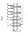
- Figure 1 is a diagram of a pattern of arrangement of bit line selection transistors in a conventional semiconductor memory device
- reference characters BL1, BL2, ..., BL8 show bit lines
- - Bl, B2, ..., B8 show decode signal lines for supplying decode signals from a column decoder circuit.
- Reference characters Fl, F2, F3, and F4 show fields on which the bit line selection transistors are formed.
- the hatched portions PSL indicate a first conductor layer, for example, a polycrystalline silicon layer. Two bit line selection transistors are formed in each field. Namely, in each
- drains are located at the right as seen in the Figure and left ends/.
- a common source is provided at the middle for the two transistors.
- the gates of the transistors are formed by the polycrystalline silicon layer PSL.
- bit line selection transistors are arranged perpendicular to the direction of the bit lines. Therefore, the pitch between adjoining bit lines is determined by the transistor width.
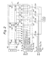
- Figure 2 is a schematic circuit diagram of a semiconductor memory device according to the preferred embodiment of the present invention.
- Figure 3 shows pattern of arrangement of bit line selection transistors on an integrated circuit substrate in the semiconductor memory device of Fig. 2.
- the semiconductor memory device of Fig. 2 comprises a memory cell region 1; a row decoder circuit (RDC) 2; word lines WL; bit line groups, each of which includes eight bit lines (BL); transistor blocks 31, 32, 33, and 34, serving as bit line selection transistor arrays, each of which includes eight bit line selection transistors QB corresponding to the bit line groups; a first column decoder circuit (CDC) 4; a second column decoder circuit (CDC) 5; block selection transistors QA; and a sense amplifier SA.
- RDC row decoder circuit
- BL bit lines
- transistor blocks 31, 32, 33, and 34 serving as bit line selection transistor arrays, each of which includes eight bit line selection transistors QB corresponding to the bit line groups
- CDC first column decoder circuit
- CDC second column decoder circuit
- block selection transistors QA and a sense amplifier SA.
- the plurality of word lines and the plurality of bit lines are arranged perpendicular to each other.
- a memory cell is located at each cross position of the word lines WL and the bit lines BL.
- Each word line WL is connected to the row decoder circuit 2.
- Each bit line BL is connected to a bit line selection transistor QB.
- the bit line selection transistors QB are separated into four blocks 31, 32, 33, and 34 corresponding to the bit line groups.
- the gates of the bit line selection transistors QB in each block are connected to column selection signal lines Bl, B2, ..., B8 from the first column decoder circuit 4, respectively.
- the first column decoder circuit 4 decodes the lower columns of address signals a 0' a 1 , a 2 and selects one of the eight column selection signal lines Bl, B2, ..., B8 to raise its potential to a high level corresponding to the pattern of the address signals a O' a 1 ,a 2 .
- the bit lines are connected together in each block through the bit line selection transistors QB. Each commonly connected line is connected to the sense amplifier circuit SA through the block selection transistors QA.
- the gates of the block selection transistors QA are connected to block selection signal lines Al, A2, A3, A4 from the second column decoder circuit 5, respectively.
- the second column decoder circuit 5 decodes upper columns of address signals a 3 , a 4 and selects one of the block selection signal lines Al, A2, A3, A4 to raise its potential to a high level corresponding to the pattern of the address signals a 3 , a 4 .
- Figure 3 is a plan view of the pattern on which the bit line selection transistors QB in the semiconductor memory device of Fig. 2 are formed.
- reference numeral 11 is a memory-cell forming region
- 12 is a decoder-circuit forming region
- 13 is a first- and second-column-decoder-circuit forming region.
- the bit line selection transistors QB are formed in pairs in rectangular fields FL.
- the bit lines from the memory-cell forming region 11 are connected to the bit selection transistors QB by an aluminum conductive pattern.
- the decode signal lines Bl, B2, ..., B8 from the first column decoder circuit 4 are connected to the bit line selection transistors QB by the polycrystalline silicon layer, arranged perpendicular to the bit lines.
- the polycrystalline silicon layer is provided above the transistor forming region with a silicon dioxide Si0 2 insulating layer inserted therebetween.
- the aluminum pattern is formed above the polycrystalline silicon layer.
- the polycrystalline silicon layer shown by the hatched lines, functions in the fields FL as gates of the bit line selection transistors QB.
- a plurality of transistor blocks are located along the direction perpendicular to the bit lines.
- the eight transistors QB included in each transistor block are arranged along the direction of the bit lines, as shown in Fig. 3.
- the gates of the bit line selection tran- sistors in the block comprised of polycrystalline silicon and connected to the decode signal lines Bl, B2, ..., B8, are thus connected to the gates of the corresponding bit line selection transistors in the adjoining transistor blocks.
- the rectangular fieldsFL' . are for forming the block selection transistors QA. In each field, two transistors QA are located.
- bit line selection transistors in each block are arranged along the direction of the bit lines, the pitch of the bit lines can be reduced to less than the width of the " region forming the bit line selection transistors.
- bit line selection transistor block the lower a bit line selection transistor is located in the figure, the less the number of crossings in the vicinity of the transistor of bit lines/. A wider contact area between the electrode of the transistor and the bit line is possible with a bit line selection transistor having less cross over. Thus, the resistance of the electric connection can be reduced and a more reliable connection achieved.
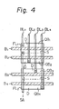
- Figure 4 is a diagram explaining the elements of the transistor pattern in Fig. 3.
- the drain of the bit line selection transistors QB1 to QB4 is shown by the reference character D.
- the source is formed in common between the bit line selection transistors QB1 and QB2 or QB3 and QB4.
- the source is indicated by the reference character S.
Landscapes
- Engineering & Computer Science (AREA)
- Microelectronics & Electronic Packaging (AREA)
- Semiconductor Memories (AREA)
- Static Random-Access Memory (AREA)
Abstract
Description
- The present invention relates to a semiconductor memory device, more particularly to a semiconductor memory device using a pattern of arrangement of elements reducing the pitch of bit lines.
- In a semiconductor memory device, a plurality of word lines and bit lines are arranged perpendicular to each other. Memory cells are located at the cross positions of each word line and bit line. Each word line is connected to a row decoder circuit. Each bit line is connected to a sense amplifier circuit through a bit line selection transistor. The gate'of each bit line selection transistor is connected to a column decoder circuit.
- Recent demand for higher density integration semiconductor memory devices has necessitated denser patterns of arrangement of word lines and bit lines. To achieve denser patterns of arrangement of bit lines, it is necessary to reduce the pitch between bit lines, which requires reducing the spacing of bit line selection transistors associated with the bit lines. embodiment
- An / of the present invention can provide a semiconductor memory device, wherein the pitch between bit lines is reduced, thereby achieving a denser pattern of arrangement of bit lines and increasing the integration density.
- According to an aspect of the present invention, there is provided a semiconductor memory device which comprises a plurality of bit line groups, each including a plurality of bit lines extending along a column direction, and a plurality of bit line selection transistor arrays each including a plurality of bit line selection transistors corresponding to the bit lines, separated into blocks corresponding to the bit line groups. In the device, the bit line selection transistor arrays are arranged perpendicular to the direction of the bit lines, the plurality of bit line selection transistors in each bit line selection transistor array are arranged along the direction of the bit lines, the gates of the bit line selection transistors are arranged perpendicular to the direction of the bit lines, and the connecting lines to the gates are extended to connect with the gates of the corresponding transistors in the adjoining bit line selection transistor arrays.
- According to another aspect of the present invention, there is provided a semiconductor memory device which comprises a plurality of word lines, a plurality of bit lines perpendicular to the word lines memory cells located at the cross positions of the word lines with the bit lines, bit line selection transistors connected to the bit lines for selecting one of the bit lines, and a sense amplifier connected to the bit line selection transistors. Column selection signals are supplied to the gates of the bit line selection transistors. In the device, the plurality of bit line selection transistors are arranged along the direction of the bit lines. The gates of the bit line selection transistors are arranged perpendicular to the direction of the bit lines.
- Reference is made, by way of example, to the accompanying drawigs in which: Figure 1 is a diagram of a pattern of arrangement of bit line selection transistors in a conventional semiconductor memory device;
- Fig. 2 is a schematic circuit diagram of a semiconductor memory device according to an embodiment of the present invention;
- Fig. 3 is a diagram of a pattern of arrangement of bit line selection transistors in the semiconductor memory device of Fig. 2; and
- Fig. 4 is a diagram explaining the pattern of arrangement of Fig. 3.
- Prior to the description of the preferred embodiment of the present invention, a pattern of'arrangement of bit line selection transistors in a conventional semiconductor memory device will be explained for comparative purposes with reference to Fig. 1.
- In Fig. 1, reference characters BL1, BL2, ..., BL8 show bit lines, and - Bl, B2, ..., B8 show decode signal lines for supplying decode signals from a column decoder circuit. Reference characters Fl, F2, F3, and F4 show fields on which the bit line selection transistors are formed. The hatched portions PSL indicate a first conductor layer, for example, a polycrystalline silicon layer. Two bit line selection transistors are formed in each field. Namely, in each
- field , drains are located at the right as seen in the Figure and left ends/. A common source is provided at the middle for the two transistors. The gates of the transistors are formed by the polycrystalline silicon layer PSL.
- In the pattern of Fig. 1, the bit line selection transistors are arranged perpendicular to the direction of the bit lines. Therefore, the pitch between adjoining bit lines is determined by the transistor width.
- Figure 2 is a schematic circuit diagram of a semiconductor memory device according to the preferred embodiment of the present invention. Figure 3 shows pattern of arrangement of bit line selection transistors on an integrated circuit substrate in the semiconductor memory device of Fig. 2.
- The semiconductor memory device of Fig. 2 comprises a
memory cell region 1; a row decoder circuit (RDC) 2; word lines WL; bit line groups, each of which includes eight bit lines (BL);transistor blocks - In the
memory cell region 1, the plurality of word lines and the plurality of bit lines are arranged perpendicular to each other. A memory cell is located at each cross position of the word lines WL and the bit lines BL. Each word line WL is connected to therow decoder circuit 2. Each bit line BL is connected to a bit line selection transistor QB. The bit line selection transistors QB are separated into fourblocks - The gates of the bit line selection transistors QB in each block are connected to column selection signal lines Bl, B2, ..., B8 from the first
column decoder circuit 4, respectively. The firstcolumn decoder circuit 4 decodes the lower columns of address signals a0' a1, a2 and selects one of the eight column selection signal lines Bl, B2, ..., B8 to raise its potential to a high level corresponding to the pattern of the address signals aO' a1 ,a2. The bit lines are connected together in each block through the bit line selection transistors QB. Each commonly connected line is connected to the sense amplifier circuit SA through the block selection transistors QA. - The gates of the block selection transistors QA are connected to block selection signal lines Al, A2, A3, A4 from the second
column decoder circuit 5, respectively. The secondcolumn decoder circuit 5 decodes upper columns of address signals a3, a4 and selects one of the block selection signal lines Al, A2, A3, A4 to raise its potential to a high level corresponding to the pattern of the address signals a3, a4. - Figure 3 is a plan view of the pattern on which the bit line selection transistors QB in the semiconductor memory device of Fig. 2 are formed. In Fig. 3,
reference numeral 11 is a memory-cell forming region, 12 is a decoder-circuit forming region, and 13 is a first- and second-column-decoder-circuit forming region. The bit line selection transistors QB are formed in pairs in rectangular fields FL. The bit lines from the memory-cell forming region 11 are connected to the bit selection transistors QB by an aluminum conductive pattern. The decode signal lines Bl, B2, ..., B8 from the firstcolumn decoder circuit 4 are connected to the bit line selection transistors QB by the polycrystalline silicon layer, arranged perpendicular to the bit lines. - Considered three dimensionally, the polycrystalline silicon layer is provided above the transistor forming region with a silicon dioxide Si02 insulating layer inserted therebetween. The aluminum pattern is formed above the polycrystalline silicon layer. The polycrystalline silicon layer, shown by the hatched lines, functions in the fields FL as gates of the bit line selection transistors QB.
- A plurality of transistor blocks are located along the direction perpendicular to the bit lines. The eight transistors QB included in each transistor block are arranged along the direction of the bit lines, as shown in Fig. 3. The gates of the bit line selection tran- sistors in the block comprised of polycrystalline silicon and connected to the decode signal lines Bl, B2, ..., B8, are thus connected to the gates of the corresponding bit line selection transistors in the adjoining transistor blocks. The rectangular fieldsFL' . are for forming the block selection transistors QA. In each field, two transistors QA are located.
- In the pattern of Fig. 3, since the bit line selection transistors in each block are arranged along the direction of the bit lines, the pitch of the bit lines can be reduced to less than the width of the "region forming the bit line selection transistors.
- Further, in a bit line selection transistor block, the lower a bit line selection transistor is located in the figure, the less the number of crossings in the vicinity of the transistor of bit lines/. A wider contact area between the electrode of the transistor and the bit line is possible with a bit line selection transistor having less cross over. Thus, the resistance of the electric connection can be reduced and a more reliable connection achieved.
- Figure 4 is a diagram explaining the elements of the transistor pattern in Fig. 3. In the figure, the drain of the bit line selection transistors QB1 to QB4 is shown by the reference character D. The source is formed in common between the bit line selection transistors QB1 and QB2 or QB3 and QB4. The source is indicated by the reference character S.
Claims (7)
Applications Claiming Priority (2)
| Application Number | Priority Date | Filing Date | Title |
|---|---|---|---|
| JP58019697A JPS59161061A (en) | 1983-02-10 | 1983-02-10 | Semiconductor memory device |
| JP19697/83 | 1983-02-10 |
Publications (3)
| Publication Number | Publication Date |
|---|---|
| EP0119002A2 true EP0119002A2 (en) | 1984-09-19 |
| EP0119002A3 EP0119002A3 (en) | 1988-01-27 |
| EP0119002B1 EP0119002B1 (en) | 1991-05-02 |
Family
ID=12006450
Family Applications (1)
| Application Number | Title | Priority Date | Filing Date |
|---|---|---|---|
| EP84300789A Expired EP0119002B1 (en) | 1983-02-10 | 1984-02-08 | Semiconductor memory device |
Country Status (4)
| Country | Link |
|---|---|
| US (1) | US4615021A (en) |
| EP (1) | EP0119002B1 (en) |
| JP (1) | JPS59161061A (en) |
| DE (1) | DE3484519D1 (en) |
Cited By (3)
| Publication number | Priority date | Publication date | Assignee | Title |
|---|---|---|---|---|
| EP0182712A3 (en) * | 1984-11-15 | 1989-08-16 | Fujitsu Limited | Semiconductor memory device |
| EP0242854A3 (en) * | 1986-04-23 | 1990-11-07 | Hitachi, Ltd. | Semiconductor memory devices |
| EP0630025A3 (en) * | 1993-06-18 | 1995-09-20 | Toshiba Kk | Semiconductor memory device. |
Families Citing this family (5)
| Publication number | Priority date | Publication date | Assignee | Title |
|---|---|---|---|---|
| JPS61110459A (en) * | 1984-11-02 | 1986-05-28 | Nippon Telegr & Teleph Corp <Ntt> | Semiconductor memory |
| US4797858A (en) * | 1987-03-30 | 1989-01-10 | Motorola, Inc. | Semiconductor memory with divided word lines and shared sense amplifiers |
| JPH0391193A (en) * | 1989-08-31 | 1991-04-16 | Fujitsu Ltd | Semiconductor storage device |
| JPH06187793A (en) * | 1992-12-18 | 1994-07-08 | Kawasaki Steel Corp | Semiconductor memory |
| US5636158A (en) * | 1995-03-13 | 1997-06-03 | Kabushiki Kaisha Toshiba | Irregular pitch layout for a semiconductor memory device |
Family Cites Families (4)
| Publication number | Priority date | Publication date | Assignee | Title |
|---|---|---|---|---|
| US3387286A (en) * | 1967-07-14 | 1968-06-04 | Ibm | Field-effect transistor memory |
| US3702466A (en) * | 1969-11-05 | 1972-11-07 | Nippon Electric Co | Semiconductor integrated circuit memory device utilizing insulated gate type semiconductor elements |
| IT1135038B (en) * | 1980-01-28 | 1986-08-20 | Rca Corp | APPARATUS TO ELECTRICALLY JOIN THE EXTREMITIES OF SEMICONDUCTOR MATERIAL LINES, SUBSTANTIALLY PARALLEL |
| JPS6059677B2 (en) * | 1981-08-19 | 1985-12-26 | 富士通株式会社 | semiconductor storage device |
-
1983
- 1983-02-10 JP JP58019697A patent/JPS59161061A/en active Granted
-
1984
- 1984-02-08 EP EP84300789A patent/EP0119002B1/en not_active Expired
- 1984-02-08 US US06/577,998 patent/US4615021A/en not_active Expired - Lifetime
- 1984-02-08 DE DE8484300789T patent/DE3484519D1/en not_active Expired - Lifetime
Cited By (3)
| Publication number | Priority date | Publication date | Assignee | Title |
|---|---|---|---|---|
| EP0182712A3 (en) * | 1984-11-15 | 1989-08-16 | Fujitsu Limited | Semiconductor memory device |
| EP0242854A3 (en) * | 1986-04-23 | 1990-11-07 | Hitachi, Ltd. | Semiconductor memory devices |
| EP0630025A3 (en) * | 1993-06-18 | 1995-09-20 | Toshiba Kk | Semiconductor memory device. |
Also Published As
| Publication number | Publication date |
|---|---|
| JPS6332271B2 (en) | 1988-06-29 |
| US4615021A (en) | 1986-09-30 |
| DE3484519D1 (en) | 1991-06-06 |
| JPS59161061A (en) | 1984-09-11 |
| EP0119002B1 (en) | 1991-05-02 |
| EP0119002A3 (en) | 1988-01-27 |
Similar Documents
| Publication | Publication Date | Title |
|---|---|---|
| US5590068A (en) | Ultra-high density alternate metal virtual ground ROM | |
| US6084794A (en) | High speed flat-cell mask ROM structure with select lines | |
| EP0169332B1 (en) | High density one device memory | |
| US5117389A (en) | Flat-cell read-only-memory integrated circuit | |
| EP0073486A2 (en) | Stacked semiconductor memory | |
| US5392233A (en) | Read only memory capable of realizing high-speed read operation | |
| KR930000761B1 (en) | Semiconductor integrated circuit device with wiring and decoder with low wiring delay | |
| EP0880144A2 (en) | Read only memory | |
| US11763872B2 (en) | 3D memory array clusters and resulting memory architecture | |
| US4615021A (en) | Semiconductor memory device | |
| US6188605B1 (en) | Non-volatile semiconductor memory using split bit lines | |
| US5602773A (en) | Memory device column address selection lead layout | |
| US6256227B1 (en) | Non-volatile semiconductor memory having column sub-selector layout pattern adaptable to miniaturization of memory cell | |
| US4584671A (en) | Semiconductor memories | |
| KR100440410B1 (en) | Texas instruments incorporated | |
| US6205044B1 (en) | Decoder connection configuration for memory chips with long bit lines | |
| US5926417A (en) | Read method for reading data from a high-density semiconductor read-only memory device | |
| US6870752B2 (en) | High density mask ROM having flat-type bank select | |
| JPH0752758B2 (en) | Semiconductor read-only memory | |
| US6798681B2 (en) | Dram | |
| JPH04305973A (en) | Semiconductor storage device | |
| KR100204537B1 (en) | A semiconductor memory device having subword line and strap structure | |
| KR960001462B1 (en) | Dynamic semiconductor memory device | |
| KR940006080B1 (en) | Word line driver of semiconductor memory aray and method of bit line aray | |
| KR960005567B1 (en) | Dram cell array |
Legal Events
| Date | Code | Title | Description |
|---|---|---|---|
| PUAI | Public reference made under article 153(3) epc to a published international application that has entered the european phase |
Free format text: ORIGINAL CODE: 0009012 |
|
| AK | Designated contracting states |
Designated state(s): DE FR GB |
|
| PUAL | Search report despatched |
Free format text: ORIGINAL CODE: 0009013 |
|
| AK | Designated contracting states |
Kind code of ref document: A3 Designated state(s): DE FR GB |
|
| 17P | Request for examination filed |
Effective date: 19880712 |
|
| 17Q | First examination report despatched |
Effective date: 19891019 |
|
| GRAA | (expected) grant |
Free format text: ORIGINAL CODE: 0009210 |
|
| AK | Designated contracting states |
Kind code of ref document: B1 Designated state(s): DE FR GB |
|
| REF | Corresponds to: |
Ref document number: 3484519 Country of ref document: DE Date of ref document: 19910606 |
|
| ET | Fr: translation filed | ||
| RTI2 | Title (correction) | ||
| PLBE | No opposition filed within time limit |
Free format text: ORIGINAL CODE: 0009261 |
|
| STAA | Information on the status of an ep patent application or granted ep patent |
Free format text: STATUS: NO OPPOSITION FILED WITHIN TIME LIMIT |
|
| 26N | No opposition filed | ||
| K2C1 | Correction of patent specification (title page) published |
Effective date: 19910502 |
|
| REG | Reference to a national code |
Ref country code: GB Ref legal event code: IF02 |
|
| PGFP | Annual fee paid to national office [announced via postgrant information from national office to epo] |
Ref country code: GB Payment date: 20020206 Year of fee payment: 19 |
|
| PGFP | Annual fee paid to national office [announced via postgrant information from national office to epo] |
Ref country code: FR Payment date: 20020212 Year of fee payment: 19 |
|
| PGFP | Annual fee paid to national office [announced via postgrant information from national office to epo] |
Ref country code: DE Payment date: 20020227 Year of fee payment: 19 |
|
| PG25 | Lapsed in a contracting state [announced via postgrant information from national office to epo] |
Ref country code: GB Free format text: LAPSE BECAUSE OF NON-PAYMENT OF DUE FEES Effective date: 20030208 |
|
| PG25 | Lapsed in a contracting state [announced via postgrant information from national office to epo] |
Ref country code: DE Free format text: LAPSE BECAUSE OF NON-PAYMENT OF DUE FEES Effective date: 20030902 |
|
| GBPC | Gb: european patent ceased through non-payment of renewal fee | ||
| PG25 | Lapsed in a contracting state [announced via postgrant information from national office to epo] |
Ref country code: FR Free format text: LAPSE BECAUSE OF NON-PAYMENT OF DUE FEES Effective date: 20031031 |
|
| REG | Reference to a national code |
Ref country code: FR Ref legal event code: ST |