EP0119281A1 - Circuit pour transmission de signaux de tension - Google Patents
Circuit pour transmission de signaux de tension Download PDFInfo
- Publication number
- EP0119281A1 EP0119281A1 EP83102431A EP83102431A EP0119281A1 EP 0119281 A1 EP0119281 A1 EP 0119281A1 EP 83102431 A EP83102431 A EP 83102431A EP 83102431 A EP83102431 A EP 83102431A EP 0119281 A1 EP0119281 A1 EP 0119281A1
- Authority
- EP
- European Patent Office
- Prior art keywords
- amplifier stage
- inverting input
- voltage
- transmitter
- receiver
- Prior art date
- Legal status (The legal status is an assumption and is not a legal conclusion. Google has not performed a legal analysis and makes no representation as to the accuracy of the status listed.)
- Granted
Links
- 230000005540 biological transmission Effects 0.000 title claims abstract description 24
- 239000003990 capacitor Substances 0.000 claims abstract description 5
- 238000001208 nuclear magnetic resonance pulse sequence Methods 0.000 description 11
- 238000010586 diagram Methods 0.000 description 4
- 238000001514 detection method Methods 0.000 description 3
- RVRCFVVLDHTFFA-UHFFFAOYSA-N heptasodium;tungsten;nonatriacontahydrate Chemical compound O.O.O.O.O.O.O.O.O.O.O.O.O.O.O.O.O.O.O.O.O.O.O.O.O.O.O.O.O.O.O.O.O.O.O.O.O.O.O.[Na+].[Na+].[Na+].[Na+].[Na+].[Na+].[Na+].[W].[W].[W].[W].[W].[W].[W].[W].[W].[W].[W] RVRCFVVLDHTFFA-UHFFFAOYSA-N 0.000 description 3
- 230000011664 signaling Effects 0.000 description 2
- 238000012935 Averaging Methods 0.000 description 1
- 230000032683 aging Effects 0.000 description 1
- 230000000694 effects Effects 0.000 description 1
- 238000011156 evaluation Methods 0.000 description 1
- 238000001914 filtration Methods 0.000 description 1
- 230000010354 integration Effects 0.000 description 1
- 238000000034 method Methods 0.000 description 1
- 238000007873 sieving Methods 0.000 description 1
- 230000001360 synchronised effect Effects 0.000 description 1
- 230000001960 triggered effect Effects 0.000 description 1
Images


Classifications
-
- H—ELECTRICITY
- H03—ELECTRONIC CIRCUITRY
- H03K—PULSE TECHNIQUE
- H03K7/00—Modulating pulses with a continuously-variable modulating signal
- H03K7/08—Duration or width modulation ; Duty cycle modulation
-
- G—PHYSICS
- G08—SIGNALLING
- G08C—TRANSMISSION SYSTEMS FOR MEASURED VALUES, CONTROL OR SIMILAR SIGNALS
- G08C19/00—Electric signal transmission systems
- G08C19/16—Electric signal transmission systems in which transmission is by pulses
- G08C19/22—Electric signal transmission systems in which transmission is by pulses by varying the duration of individual pulses
Definitions
- the invention relates to a circuit arrangement for the transmission of voltage signals from a transmitter via a transmission link to a receiver.
- the modem generally includes the complete control with which the data traffic is controlled, as well as a synchronous or an asynchronous data buffer, which converts the pending parallel data to a serial bit stream on the transmitter side and provides start, parity and stop bits and the serial data stream on the receiver side parallelized again; the measured value must then be recovered using a digital-to-analog converter.
- This effort may make sense for industrial and commercial data transmission. In many cases, however, cost-effective data transmission and preferably analog value transmission is desirable and the effort described above is no longer justified.
- the invention has for its object to provide a circuit arrangement of the type mentioned, which allows voltage or current signals to be transmitted without interference at very little effort, even over larger distances by quasi digital data transmission without losses.
- the invention provides that a first amplifier stage with an inv ting and a non-inverting input is provided, the output of which is fed back to the inverting input via a capacitor, the negative operating voltage of the circuit and the voltage signal are connected to the inverting input of the first amplifier stage via the series connection of two resistors, the non-inverting input the first amplifier stage is connected to the ground potential between the positive and the negative operating voltage, a second amplifier stage is provided with an inverting and a non-inverting input, the inverting input of which is connected via a resistor to the output of the first amplifier stage and the output signal of which Receiver is transmitted, the output of the second amplifier stage via the series connection of two resistors to the ground potential and their connection point to the non-inverting input of the second amplifier stage, a switch r is provided which, depending on a predeterminable size of the output signal of the second amplifier stage, switches the connection point between the resistors which are arranged between the inverting input of the first amplifier stage and
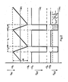
- the pulse duty factor T t l / (t l + t Z ) is proportional to the instantaneous value of the signal value and as a pulse train is placed on the transmission link.
- the pulse duty factor T t l / (t l + t Z ) is proportional to the instantaneous value of the signal value and as a pulse train is placed on the transmission link.
- the pulse duty factor T t l / (t l + t Z ) is proportional to the instantaneous value of the signal value and as a pulse train is placed on the transmission link.
- the pulse duty factor of which depends on the signal value by sieving with a low-pass filter
- This quasi-digitized signal value can now be transmitted losslessly over longer distances.
- the arithmetic mean value can be formed from this again by a simple active or passive low-pass filter, so that the analog signal value recovered at the receiver is again exactly proportional to the incoming duty cycle, which represents the input signal value.
- the entire circuit arrangement according to the invention is self-compensating. This means that aging, drift, component changes, operating voltage changes or similar effects have no influence on the transmission accuracy.
- a first amplifier stage as a summation integrator and a second amplifier stage as a comparator with hysteresis are connected together on the transmitter side in such a way that an existing analog signal value is converted into an equivalent pulse sequence with the properties described above.
- a low-pass filter averages the pulse duty factor and thus recovers the input signal.
- the integrated components provided by the electronics can be used with advantage, so that an arrangement is obtained which can be produced extremely cheaply, but nevertheless enables reliable measured value transmission even over longer distances.
- a two-wire line can be used as the transmission path between the transmitter and the receiver, via which the supply voltage is also supplied to the transmitter.
- means can be provided with particular advantage on the transmitter side in order to key the current flowing on the two-wire line between two values in accordance with the useful signal.
- a shunt resistor placed between the two wires is preferably used on the transmitter side and is connected in series with a switch which is triggered by the pulse sequence generated.
- a current sensor is then provided on the receiver side, which reconstructs the useful signal from the two current values.
- a current is advantageously used as a current sensor in a resistor that is looped into one of the wires of the two-wire line and whose pulse-shaped voltage drop is evaluated.
- an amplitude comparator for example a window comparator, which measures the discrete voltages generated by the low-pass filter assigned to each of these switching function, the result is an extremely simple means of a powerful signaling system with the possibility of individual identification of several detectors switched on a single transmission path or line.
- FIG. 1 shows a measuring voltage is to be transferred, which might be derived by a voltage divider or potentiometer of the voltage + U B to simply as xU B, ie shown as part of the positive operating voltage + U B.
- This measuring voltage is fed via a resistor R1 to the inverting input (-) of an amplifier stage IC1, which can be designed as an operational amplifier and which in this exemplary embodiment has a positive operating voltage (+ U B ) and a negative operating voltage (-U B ) against ground potential GND is fed.
- the output A1 of the amplifier stage IC1 is fed back via a capacitor C to the inverting input (-); the amplifier stage IC1 thus works as an integrator.
- the non-inverting input (+) of the amplifier stage IC1 is connected to the ground potential GND.
- the negative operating voltage (-U B ) is also fed to the inverting input () of the amplifier stage IC1 via the series connection of two resistors R2 'and R2 ". This arrangement creates a summation integrator.
- the output A1 of the amplifier stage IC1 is connected via a resistor R3 to the inverting input (-) of a second amplifier stage IC2, which is likewise fed from the positive and the negative operating voltage source (+ U B , -U B ).
- the output A2 of the second amplifier stage IC2 is connected via a resistor R5 to its non-inverting input (+) and this is connected to the ground potential GND via a resistor R4.
- the second amplifier stage IC2 works as a comparator with a hysteresis value formed by the resistance ratio R4 / R5.
- a resistor R6 leads from the output A2 of the second amplifier stage IC2 to the base of a PNP transistor T1, which works as a switch and can connect the common connection of the resistors R2 'and R2 "to the ground potential GND.
- Resistor R1 is permanently due to a partial size of U B , ie xU B. This voltage is applied to the inverting input (-) of the amplifier stage IC1, which operates as a summing integrator. It is first assumed that the transistor T1 is turned on. The capacitor C is then charged with a time-constant current, so that the output voltage U A1 of the integrator drops in a time-linear manner from + U k to -U k . If the output voltage U Al of the integrator now reaches the switching threshold -U k of the comparator, the output voltage U A2 of the comparator jumps from the negative saturation value U s to the positive saturation value U +, so that the PNP transistor T1 is blocked.
- the negative operating voltage -U B is now at the summation point of the integrator via the resistors R2 'and R2 ", and there is a back integration until the output voltage U A1 of the integrator has reached the positive switching threshold U k of the comparator, the output voltage U A2 of which jumps then back to the negative saturation voltage U-.
- the transistor T1 is now switched on again, and the process described begins anew.
- the duty cycle is therefore an exact measure of the measuring voltage at the circuit input.
- amplifiers whose supply voltages + U B , -U B are symmetrical or also asymmetrical to the ground potential
- amplifier circuits whose positive supply voltage is a voltage + U B and whose negative supply connection is connected to the potential GND .
- a medium voltage between the potentials + U B and GND for the non-inverting input (+) of the amplifier IC1 can then be generated with a suitably dimensioned voltage divider.
- the pulse sequence at the output of the second amplifier stage IC2 which works as a comparator, can now be applied, for example, directly to a transmission path L in the form of a wire line to the receiver input.
- the receiver is a low pass.
- the arithmetic mean of the pulsating DC voltage applied to the input is obtained at its output. This mean value is then proportional to the input voltage.
- the pulse sequence generated according to the invention and corresponding to the measured value can also be used to carry out the measured value transmission by means of a radio link.
- an oscillator oscillating at a suitable frequency must be modulated in frequency or phase with the pulse train.
- An FM or PM demodulator is then provided on the receiver side, which delivers a pulse sequence in which the edges occur in exactly the same time assignment as in the modulating pulse sequence in the transmitter.
- the 220-volt power network can also serve as a transmission path using a suitable network adapter.
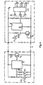
- the pulse sequence generated in the transmitter S is preferably used to control circuit means with which the current flowing on the two-wire line is switched back and forth between two current values in a defined manner, that is to say is keyed.
- a suitable arrangement for this is, for example, a shunt resistor R S lying in series with a switch between the two wires of the line (FIG. 3).
- This switch which is preferably a transistor T4 (FIG.
- a current sensor is provided on the receiver side, which in the embodiment shown here is a resistor R L , which is looped into one of the wires of the line, the voltage drop of which is also pulse-shaped. If, for example, the base-emitter path of a transistor is placed over this resistor R L , the transistor T3 is turned on or off according to the incoming current pulses. The pulses resulting at the collector of the transistor correspond in time sequence to those of the transmitter pulses; their duty cycle is proportional to the measuring voltage. The measured value is obtained from them by low-pass filtering.
- the measuring voltage can be the voltage which a sensor which responds to a physical quantity (temperature, pressure, etc.) supplies and which can be amplified.
- the switching transistor T4, the shunt resistor R s and the resistor R L serving as a current sensor perform the same functions as in the embodiment of the invention shown in FIG. 3.
- the low-pass filter generates output voltages with discrete values proportional to the pulse duty factor of the incoming pulse sequence, which quasi-digitize in a window comparator F working as an al-s amplitude discriminator and via an evaluation logic and driver stage LT for signaling in a transmitter-mounted switch S1 to Allow the assigned channel to be used, e.g. to excite one of the switching relays Kl to K3.
- FIG. 4 An arrangement according to FIG. 4 gives the possibility of individual identification of a plurality of detectors connected to a common detection line. This aspect is essential in hazard detection technology if the effort to be made for a detection system must not impair the security to be achieved.
Landscapes
- Physics & Mathematics (AREA)
- General Physics & Mathematics (AREA)
- Arrangements For Transmission Of Measured Signals (AREA)
- Selective Calling Equipment (AREA)
- Amplifiers (AREA)
Priority Applications (3)
| Application Number | Priority Date | Filing Date | Title |
|---|---|---|---|
| AT83102431T ATE28250T1 (de) | 1983-03-11 | 1983-03-11 | Schaltungsanordnung zur uebertragung von spannungssignalen. |
| EP83102431A EP0119281B1 (fr) | 1983-03-11 | 1983-03-11 | Circuit pour transmission de signaux de tension |
| DE8383102431T DE3372419D1 (en) | 1983-03-11 | 1983-03-11 | Circuitry for the transmission of voltage signals |
Applications Claiming Priority (1)
| Application Number | Priority Date | Filing Date | Title |
|---|---|---|---|
| EP83102431A EP0119281B1 (fr) | 1983-03-11 | 1983-03-11 | Circuit pour transmission de signaux de tension |
Publications (2)
| Publication Number | Publication Date |
|---|---|
| EP0119281A1 true EP0119281A1 (fr) | 1984-09-26 |
| EP0119281B1 EP0119281B1 (fr) | 1987-07-08 |
Family
ID=8190341
Family Applications (1)
| Application Number | Title | Priority Date | Filing Date |
|---|---|---|---|
| EP83102431A Expired EP0119281B1 (fr) | 1983-03-11 | 1983-03-11 | Circuit pour transmission de signaux de tension |
Country Status (3)
| Country | Link |
|---|---|
| EP (1) | EP0119281B1 (fr) |
| AT (1) | ATE28250T1 (fr) |
| DE (1) | DE3372419D1 (fr) |
Cited By (4)
| Publication number | Priority date | Publication date | Assignee | Title |
|---|---|---|---|---|
| DE3624663A1 (de) * | 1986-07-22 | 1988-01-28 | Bosch Gmbh Robert | Schaltungsanordnung zum ein- und ausschalten unterschiedlicher elektrischer verbraucher |
| EP0525372A1 (fr) * | 1991-07-26 | 1993-02-03 | Mario Bellini | Méthode de transmission de signaux analogiques sous forme numérique dans des applications d'automatisation industrielle |
| GB2279193A (en) * | 1993-06-16 | 1994-12-21 | Smiths Industries Plc | Pulse width modulators |
| WO2002075923A3 (fr) * | 2001-03-20 | 2003-02-27 | Honeywell Int Inc | Circuit permettant de convertir une tension en un cycle de service lineaire |
Families Citing this family (1)
| Publication number | Priority date | Publication date | Assignee | Title |
|---|---|---|---|---|
| DE3543280C2 (de) * | 1984-12-21 | 1994-07-07 | Vaillant Joh Gmbh & Co | Schaltung zur Erzeugung eines linear von einem langsam veränderlichen Eingangssignal abhängigen Pulspausensignals |
Citations (5)
| Publication number | Priority date | Publication date | Assignee | Title |
|---|---|---|---|---|
| US2837642A (en) * | 1953-12-17 | 1958-06-03 | Bell Telephone Labor Inc | Pulse rate discriminator |
| GB910787A (en) * | 1958-02-13 | 1962-11-21 | Emi Ltd | Improvements relating to pulse width modulators |
| US3705363A (en) * | 1970-09-26 | 1972-12-05 | Sony Corp | Control signal generator with selectively switchable duration control circuit |
| US4117411A (en) * | 1977-09-26 | 1978-09-26 | Moore Products Co. | Isolation circuit with duty cycle feedback |
| DE2732298A1 (de) * | 1977-07-16 | 1979-02-01 | Bosch Gmbh Robert | Vorrichtung zur erzeugung einer impulsfolge mit in abhaengigkeit von einer steuerspannung einstellbarem tastverhaeltnis |
-
1983
- 1983-03-11 DE DE8383102431T patent/DE3372419D1/de not_active Expired
- 1983-03-11 AT AT83102431T patent/ATE28250T1/de not_active IP Right Cessation
- 1983-03-11 EP EP83102431A patent/EP0119281B1/fr not_active Expired
Patent Citations (5)
| Publication number | Priority date | Publication date | Assignee | Title |
|---|---|---|---|---|
| US2837642A (en) * | 1953-12-17 | 1958-06-03 | Bell Telephone Labor Inc | Pulse rate discriminator |
| GB910787A (en) * | 1958-02-13 | 1962-11-21 | Emi Ltd | Improvements relating to pulse width modulators |
| US3705363A (en) * | 1970-09-26 | 1972-12-05 | Sony Corp | Control signal generator with selectively switchable duration control circuit |
| DE2732298A1 (de) * | 1977-07-16 | 1979-02-01 | Bosch Gmbh Robert | Vorrichtung zur erzeugung einer impulsfolge mit in abhaengigkeit von einer steuerspannung einstellbarem tastverhaeltnis |
| US4117411A (en) * | 1977-09-26 | 1978-09-26 | Moore Products Co. | Isolation circuit with duty cycle feedback |
Non-Patent Citations (3)
| Title |
|---|
| ELECTRONIC ENGINEERING, Band 43, Nr. 526, Dezember 1971, Seiten 36-38, London, GB. * |
| IEEE TRANSACTIONS ON INDUSTRIAL ELECTRONICS AND CONTROL INSTRUMENTATION, Band IECI-26, Nr. 3, August 1979, Seiten 166-172, IEEE, New York, USA * |
| MEDICAL AND BIOLOGICAL ENGINEERING, Band 13, Nr. 4, Juli 1975, Seiten 544-550, Stevenage, GB. * |
Cited By (6)
| Publication number | Priority date | Publication date | Assignee | Title |
|---|---|---|---|---|
| DE3624663A1 (de) * | 1986-07-22 | 1988-01-28 | Bosch Gmbh Robert | Schaltungsanordnung zum ein- und ausschalten unterschiedlicher elektrischer verbraucher |
| EP0525372A1 (fr) * | 1991-07-26 | 1993-02-03 | Mario Bellini | Méthode de transmission de signaux analogiques sous forme numérique dans des applications d'automatisation industrielle |
| GB2279193A (en) * | 1993-06-16 | 1994-12-21 | Smiths Industries Plc | Pulse width modulators |
| FR2706700A1 (fr) * | 1993-06-16 | 1994-12-23 | Smiths Industries Plc | Dispositif et procédé de traitement de deux signaux d'entrée. |
| GB2279193B (en) * | 1993-06-16 | 1997-12-17 | Smiths Industries Plc | Signal processing |
| WO2002075923A3 (fr) * | 2001-03-20 | 2003-02-27 | Honeywell Int Inc | Circuit permettant de convertir une tension en un cycle de service lineaire |
Also Published As
| Publication number | Publication date |
|---|---|
| EP0119281B1 (fr) | 1987-07-08 |
| ATE28250T1 (de) | 1987-07-15 |
| DE3372419D1 (en) | 1987-08-13 |
Similar Documents
| Publication | Publication Date | Title |
|---|---|---|
| DE68923280T2 (de) | Funkübertragunssystem im zeitbereich. | |
| DE19753472B4 (de) | Photoelektrische Zelle mit stabilisierter Verstärkung | |
| DE1245418B (de) | Ohne Bezugswert arbeitender Impulsphasen-Demodulator | |
| DE2253015A1 (de) | Breitbanddiskriminator | |
| EP0119281B1 (fr) | Circuit pour transmission de signaux de tension | |
| DE2713443A1 (de) | Analog-digital-wandler, der ein pulsdichtemoduliertes ausgangssignal liefert | |
| DE3503885A1 (de) | Sender/empfaenger | |
| DE3214978C2 (fr) | ||
| DE3234152C2 (fr) | ||
| EP0231980B1 (fr) | Méthode pour la transmission de signaux de mesure d'au moins deux transducteurs par liaison à transmission optique | |
| DE2101887C2 (de) | Beschleunigungsmesser | |
| DE3689556T2 (de) | Gerät und Verfahren zur Umwandlung einer Spannung in einen digitalen Zählwert. | |
| DE2719937A1 (de) | Messvorrichtung zur drahtlosen erfassung von messwerten aus einer elektrischen anlage | |
| DE2722581A1 (de) | Schaltungsanordnung zur signalaufbereitung von ausgangssignalen eines feldplattengebers bei raddrehzahlgebern von fahrzeugen | |
| DE2325191C3 (fr) | ||
| DE3117927C2 (de) | Anordnung zur Erkennung der längsten von in digitalen Signalen periodisch enthaltenen Folgen von Nullzeichen | |
| CH648168A5 (de) | Elektronischer sender fuer gleichstromtelegraphiesysteme. | |
| DE2134956B2 (de) | Diskriminatoranordnung für Datenmodems einer doppelseitig gerichteten Zweidraht-Datenübertragungseinrichtung mit Frequenzmodulation | |
| DE2604925C2 (de) | Schaltungsanordnung mit einem Präzisionsmodulator | |
| EP0387685A2 (fr) | Procédé de conversion de tension en fréquence et dispositif de réalisation dudit procédé | |
| DE1283364B (de) | Anordnung zur UEbertragung einer aus einem auf der Hochspannungsseite fliessenden Strom abgeleiteten Spannung von der Hochspannungs- auf die Niederspannungsseite | |
| DE4211430C1 (de) | Schaltungsanordnung zur Erzeugung eines zeitvariablen Ausgangssignals | |
| DE2736522C2 (de) | Schaltungsanordnung zum Obertragen von Daten | |
| DE2442822B2 (de) | Schaltungsanordnung zur Messung von auf Datenübertragungsstrecken auftretenden Pegelunterbrechungen und Pegelabsenkungen | |
| DE2523373B2 (de) | Schaltungsanordnung zur uebertragung von impulsartigen signalen ueber das koppelfeld einer zeitmultiplex-vermittlungsanlage |
Legal Events
| Date | Code | Title | Description |
|---|---|---|---|
| PUAI | Public reference made under article 153(3) epc to a published international application that has entered the european phase |
Free format text: ORIGINAL CODE: 0009012 |
|
| 17P | Request for examination filed |
Effective date: 19830311 |
|
| AK | Designated contracting states |
Designated state(s): AT BE CH DE FR GB IT LI LU NL SE |
|
| GRAA | (expected) grant |
Free format text: ORIGINAL CODE: 0009210 |
|
| AK | Designated contracting states |
Kind code of ref document: B1 Designated state(s): AT BE CH DE FR GB IT LI LU NL SE |
|
| REF | Corresponds to: |
Ref document number: 28250 Country of ref document: AT Date of ref document: 19870715 Kind code of ref document: T |
|
| REF | Corresponds to: |
Ref document number: 3372419 Country of ref document: DE Date of ref document: 19870813 |
|
| RAP2 | Party data changed (patent owner data changed or rights of a patent transferred) |
Owner name: FRITZ FUSS GMBH & CO. |
|
| ET | Fr: translation filed | ||
| REG | Reference to a national code |
Ref country code: CH Ref legal event code: PFA Free format text: FRITZ FUSS GMBH & CO. |
|
| ITF | It: translation for a ep patent filed | ||
| BECN | Be: change of holder's name |
Effective date: 19870708 |
|
| ET1 | Fr: translation filed ** revision of the translation of the patent or the claims | ||
| PLBE | No opposition filed within time limit |
Free format text: ORIGINAL CODE: 0009261 |
|
| STAA | Information on the status of an ep patent application or granted ep patent |
Free format text: STATUS: NO OPPOSITION FILED WITHIN TIME LIMIT |
|
| 26N | No opposition filed | ||
| REG | Reference to a national code |
Ref country code: FR Ref legal event code: CD |
|
| ITTA | It: last paid annual fee | ||
| EPTA | Lu: last paid annual fee | ||
| EAL | Se: european patent in force in sweden |
Ref document number: 83102431.0 |
|
| PGFP | Annual fee paid to national office [announced via postgrant information from national office to epo] |
Ref country code: GB Payment date: 19950303 Year of fee payment: 13 |
|
| PGFP | Annual fee paid to national office [announced via postgrant information from national office to epo] |
Ref country code: SE Payment date: 19960301 Year of fee payment: 14 |
|
| PG25 | Lapsed in a contracting state [announced via postgrant information from national office to epo] |
Ref country code: GB Effective date: 19960311 |
|
| PGFP | Annual fee paid to national office [announced via postgrant information from national office to epo] |
Ref country code: BE Payment date: 19960311 Year of fee payment: 14 |
|
| PGFP | Annual fee paid to national office [announced via postgrant information from national office to epo] |
Ref country code: FR Payment date: 19960329 Year of fee payment: 14 |
|
| PGFP | Annual fee paid to national office [announced via postgrant information from national office to epo] |
Ref country code: NL Payment date: 19960331 Year of fee payment: 14 |
|
| GBPC | Gb: european patent ceased through non-payment of renewal fee |
Effective date: 19960311 |
|
| PG25 | Lapsed in a contracting state [announced via postgrant information from national office to epo] |
Ref country code: SE Effective date: 19970312 |
|
| PG25 | Lapsed in a contracting state [announced via postgrant information from national office to epo] |
Ref country code: BE Effective date: 19970331 |
|
| BERE | Be: lapsed |
Owner name: FRITZ FUSS G.M.B.H. & CO. Effective date: 19970331 |
|
| PG25 | Lapsed in a contracting state [announced via postgrant information from national office to epo] |
Ref country code: NL Effective date: 19971001 |
|
| PG25 | Lapsed in a contracting state [announced via postgrant information from national office to epo] |
Ref country code: FR Free format text: LAPSE BECAUSE OF NON-PAYMENT OF DUE FEES Effective date: 19971128 |
|
| NLV4 | Nl: lapsed or anulled due to non-payment of the annual fee |
Effective date: 19971001 |
|
| EUG | Se: european patent has lapsed |
Ref document number: 83102431.0 |
|
| REG | Reference to a national code |
Ref country code: FR Ref legal event code: ST |
|
| PGFP | Annual fee paid to national office [announced via postgrant information from national office to epo] |
Ref country code: LU Payment date: 19980331 Year of fee payment: 16 |
|
| PGFP | Annual fee paid to national office [announced via postgrant information from national office to epo] |
Ref country code: CH Payment date: 19990302 Year of fee payment: 17 |
|
| PG25 | Lapsed in a contracting state [announced via postgrant information from national office to epo] |
Ref country code: LU Free format text: LAPSE BECAUSE OF NON-PAYMENT OF DUE FEES Effective date: 19990311 |
|
| PGFP | Annual fee paid to national office [announced via postgrant information from national office to epo] |
Ref country code: AT Payment date: 19990331 Year of fee payment: 17 |
|
| PG25 | Lapsed in a contracting state [announced via postgrant information from national office to epo] |
Ref country code: AT Free format text: LAPSE BECAUSE OF NON-PAYMENT OF DUE FEES Effective date: 20000311 |
|
| PG25 | Lapsed in a contracting state [announced via postgrant information from national office to epo] |
Ref country code: LI Free format text: LAPSE BECAUSE OF NON-PAYMENT OF DUE FEES Effective date: 20000331 Ref country code: CH Free format text: LAPSE BECAUSE OF NON-PAYMENT OF DUE FEES Effective date: 20000331 |
|
| REG | Reference to a national code |
Ref country code: CH Ref legal event code: PL |
|
| PGFP | Annual fee paid to national office [announced via postgrant information from national office to epo] |
Ref country code: DE Payment date: 20010328 Year of fee payment: 19 |
|
| PG25 | Lapsed in a contracting state [announced via postgrant information from national office to epo] |
Ref country code: DE Free format text: LAPSE BECAUSE OF NON-PAYMENT OF DUE FEES Effective date: 20021001 |