EP0119584B1 - Circuit d'allumage pour lampe à décharge électrique - Google Patents
Circuit d'allumage pour lampe à décharge électrique Download PDFInfo
- Publication number
- EP0119584B1 EP0119584B1 EP19840102738 EP84102738A EP0119584B1 EP 0119584 B1 EP0119584 B1 EP 0119584B1 EP 19840102738 EP19840102738 EP 19840102738 EP 84102738 A EP84102738 A EP 84102738A EP 0119584 B1 EP0119584 B1 EP 0119584B1
- Authority
- EP
- European Patent Office
- Prior art keywords
- voltage
- lamp
- switching device
- inverter
- lighting circuit
- Prior art date
- Legal status (The legal status is an assumption and is not a legal conclusion. Google has not performed a legal analysis and makes no representation as to the accuracy of the status listed.)
- Expired
Links
Images









Classifications
-
- H—ELECTRICITY
- H05—ELECTRIC TECHNIQUES NOT OTHERWISE PROVIDED FOR
- H05B—ELECTRIC HEATING; ELECTRIC LIGHT SOURCES NOT OTHERWISE PROVIDED FOR; CIRCUIT ARRANGEMENTS FOR ELECTRIC LIGHT SOURCES, IN GENERAL
- H05B41/00—Circuit arrangements or apparatus for igniting or operating discharge lamps
- H05B41/14—Circuit arrangements
- H05B41/36—Controlling
- H05B41/38—Controlling the intensity of light
- H05B41/39—Controlling the intensity of light continuously
- H05B41/392—Controlling the intensity of light continuously using semiconductor devices, e.g. thyristor
-
- H—ELECTRICITY
- H05—ELECTRIC TECHNIQUES NOT OTHERWISE PROVIDED FOR
- H05B—ELECTRIC HEATING; ELECTRIC LIGHT SOURCES NOT OTHERWISE PROVIDED FOR; CIRCUIT ARRANGEMENTS FOR ELECTRIC LIGHT SOURCES, IN GENERAL
- H05B41/00—Circuit arrangements or apparatus for igniting or operating discharge lamps
- H05B41/14—Circuit arrangements
- H05B41/26—Circuit arrangements in which the lamp is fed by power derived from DC by means of a converter, e.g. by high-voltage DC
- H05B41/28—Circuit arrangements in which the lamp is fed by power derived from DC by means of a converter, e.g. by high-voltage DC using static converters
- H05B41/282—Circuit arrangements in which the lamp is fed by power derived from DC by means of a converter, e.g. by high-voltage DC using static converters with semiconductor devices
Definitions
- This invention relates to a lighting circuit for an electric discharge lamp having the features of the preamble of claim 1.
- the switching device is arranged to periodically stop energisation of the discharge lamp by the control device in that the switching device is switched ON and OFF for bringing the lamp to flash.
- GB-A-2,073,520 discloses a switching device having a control circuit.
- the switching device supplies a commercial voltage to the discharge lamp.
- the discharge lamp is fed in intervals around the maximum instantaneous value of the supplied commercial voltage.
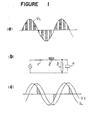
- Japanese unexamined utility model publication No. 4779/1973 discloses a lighting circuit of a construction, in which use is made of a turn-off thyristor provided in parallel with a fluorescent lamp to thereby convert a lamp voltage V L in a sinusoidal waveform into a plurality of pulse voltage as shown in Figure 1(a) of the accompanying drawing.
- This lamp voltage V L is of commercial frequency, the purpose of which is to reduce a size of a choking coil as a current limiting impedance, hence the prior art invention differs from the present invention.
- JP-A-36786/1976 discloses an improved technique, wherein the pulse voltage is made in an alternate direction.
- This prior right invention also aims at size-reduction of the choking coil, the frequency band for use of which is different from that of the present invention, hence no improvement can be attained in the operating efficiency of the low pressure electric discharge tube to be mentioned later.
- JP-A-115078/1976 discloses a lighting circuit for a fluorescent lamp having a capacitive current limiting impedance composed of a serial connection of a capacitor 1 and a choking coil 2 as shown in Figure 1 (b), wherein a switching device 4 is provided in parallel with a lamp 3 to effect short-circuiting of the switching device once every half cycle at the trailing part (those hatch-lined portions in Figure 1(c)) of the lamp current I L in a sinusoidal waveform of a commercial frequency.
- This disclosed art is, however, to facilitate restrike of the electric discharge lamp by increasing a charging voltage V c of the capacitor 1 at the time of the restriking.
- US-A-3,789,266 discloses improvement in efficiency of the abovementioned electric discharge lamp, wherein a high frequency interrupted current having a conduction period T 1 and a breaking period (hereinafter called "pause-time period") To, and the current direction of which reserves at every changing of the conduction period and the pause-time period.
- a device for flowing electric current such as mentioned above is limited to a circuit shown in Figure 2(b).
- This circuit is constructed with a bridge circuit, in which transistors 5, 6, 7 and 8 are arranged on four sides and an electric discharge lamp 9 is connected across the diagonal line; another transistor 10 provided in series with the input side of the bridge circuit; and a control device 11 which performs controls of opening and closing of the transistors 5, 6, 7, 8, and 10 to thereby cause electric current to flow as shown in Figure 2(a).
- the voltage to be applied to the transistors 5, 6, 7 and 8 is a rectangular waveform, at a high voltage portion of which the pause-time period To is formed by the transistor 10 with the consequent disadvantages such that the capacity of the device should essentially be made larger, and that the radio noise is also high.
- the low pressure mercury-vapor electric discharge lamp such as fluorescent lamp with a high frequency voltage having the pause-time period as disclosed in JP-A-196497/1982 and Japanese patent application No. 110369/1981
- the present inventors have discovered that the lamp efficiency can be further improved from the values as shown in the above-discussed US-A-3789266.
- a pause-time period To is formed at least at a rising part of its sinusoidal output voltage where an instantaneous value is small, and the electric power is supplied to the above-mentioned low pressure electric discharge lamp at a portion where the instantaneous value of the above-mentioned output voltage is large, thereby increasing efficiency of the abovementioned low pressure electric discharge lamp, and reducing the radio noise with the lighting circuit of a relatively small capacity.
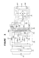
- a reference numeral 12 designates a commercial alternating current power source
- a numeral 13 refers to a rectifying device for the full-wave rectification of the power source 12
- a numeral 14 refers to a smoothing capacitor
- a reference numeral 15 denotes a high frequency inverter to energize a fluorescent lamp 16 as a low pressure electric discharge lamp.
- a self-excited, constant current type push-pull transistor inverter there is used.
- the inverter 15 is constructed as mentioned in the following: a high frequency choking coil 17 provided at the input terminal of the inverter 15; an output transformer 18; the primary windings 18a, 18b, at the junction of which the high frequency choking coil 17 is connected a feedback winding 18c; a secondary winding 18s; pre-heating windings 18f, 18f to preheat the preheating type electrodes 16f, 16f of lamp 16; a power source winding 18d of a control device 19 to be described later; a resonating capcaitor 20 connected in parallel with the primary windings 18a, 18b; a pair of transistors 21a, 21b as the active components connected between the primary windings 18a, 18b and the negative terminal of the capacitor 14; a pair of base resistors 22a, 22b; and a choking coil 23 which functions as a current limiting impedance to the electric current flowing through the lamp 16.
- a reference letter A designates a switching device provided in parallel with the lamp 16 at the output terminals of the inverter 15, and includes with a full-wave rectification circuit 24, the alternating current terminals of which are connected in parallel with the lamp 16, and a transistor 25 disposed at the direct current terminals of this rectification circuit 24.
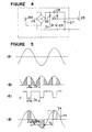
- FIG. 4 is a circuit diagram showing one embodiment of the control device 19 for the transistor 25.
- a reference numeral 18d designates the power source winding provided in the transformer 18
- a numeral 26 refers to a diode bridge which performs the full-wave rectification of a high frequency of a low voltage induced in the winding 18d
- a reference numeral 27 represents a smoothing capacitor connected with the output terminal of the diode bridge 26 through a back-flow preventing diode 28
- a reference numeral 29 denotes a transistor connected in parallel with the capacitor 27 through a resistor 30, which transistor 29 is also disposed between the base and the emitter of the transistor 25.
- a reference numeral 31 designates a constant voltage diode connected with the base of the transistor 29 through a resistor 32.
- the inverter 15 when a voltage is applied to it from the power source 12, a smoothed direct current formed by the rectification device rectifier 13 and the capacitor 14 is introduced as an input into the inverter 15, whereby the transistors 21a, 21b are opened and closed alternately by the actions of the primary windings 18a, 18b, the resonating capacitor 20, the feedback winding 18c, and so forth, and the inverter 15 starts its self- oscillation.
- the collector current of the transistors 21a, 21b b is rendered to be in a substantially rectangular waveform by the action of the high frequency choking coil 17, whereby the voltage in the primary windings 18a,18b assumes a substantially sinusoidal waveform.
- a voltage across the collector and the emitter of the transistor 29 takes a shape as shown in Figure 5(c), while the transistor 25 becomes conductive at the trailing part T 01 and the rising part T 02 of the output voltage in the secondary windings 18s in a substantially sinusoidal waveform (in general, a high harmonic component is superposed in it to some extent) as shown in Figure 5(d) to thereby form the pause-time period To, and it is interrupted during a period T 1 in the vicinity of the maximum instantaneous value of the output voltage, whereby a voltage as shown by a hatch-lined portion in Figure 5(d) is applied to the lamp 16.
- the electrodes 16f are preheated by a voltage in the sinusoidal waveform which has been induced in the preheating windings 18f, and, as soon as the electrodes 16f are heated to a predetermined temperature level, the lamp 16 is lit.
- the voltage to be applied to the lamp 16 i.e., the voltage in the hatch-lined portion in Figure 5(d)
- the voltage to be applied to the lamp 16 lowers for a portion of a voltage drop in the choking coil 23, although it hardly changes during the time periods of T,, To,, T o2 , and To.
- a starting voltage for the lamp 16 at its high frequency operating is in general higher than in the case of the commercial frequency operating, and the voltage for operating the lamp is low, on account of which the inverter 15 has a constant current characteristic at the output side, and the output current of the inverter 15 assumes a substantially continuous sinusoidal waveform at the time of both conduction and interruption of the transistor 25.
- the output current is in substantially the same waveform as that shown in Figure 5(d), the blank portion indicating a short-circuit current flowing in the switching device A, and the hatch-lined portion indicating a lamp current flowing in the lamp 16.
- the lamp current takes a triangular waveform with gentle rising
- the lamp current takes a triangular waveform with gentle trailing, both cases not being able to afford sufficient lamp efficiency, and the efficiency being particularly low in the former case.
- the circuit construction of this embodiment of the present invention wherein the switching device A is provided in parallel with the lamp 16, even if the constant current characteristic at the output side of the inverter 15, for example, is not so perfect as mentioned in the foregoing, there can be obtained fair waveforms with steep rising part as shown by the hatch-lined portions in Figure 5(d) for both voltage and current of the lamp 16 by the counter-electromotive force of the current limiting impedance 23 due to the short-circuit current, irrespective of whether the current limiting impedance 23 is resistance, inductance, or capacitance, whereby the operating efficiency of the lamp 16 improves remarkably.
- the output voltage from the bridge type inverter shown in Figure 2(b) is in a rectangular waveform V A as shown in the right half of Figure 5(d), in contrast to which the output voltage from the inverter 15 is in a sinusoidal waveform as designated by V s in Figure 5(d).
- V A the output voltage from the bridge type inverter shown in Figure 2(b)
- the sinusoidal waveform of the latter has its pause-time period To formed at a relatively small portion of the instantaneous voltage value, its output capacity can be smaller than the former.
- the transistors 10 and 25 both perform their respective switching operations at a substantially same voltage and with a substantially same current, hence the switching loss may be substantially equal between both transistors.
- the collector current of the transistors 21a, 21b is in a rectangular half waveform as shown in Figure 6(a), but their voltage between the collector and the emitter is in a sinusoidal half waveform as shown in Figure 6(b), so that their switching loss is theoretically non-existent. Accordingly, the overall efficiency of the lighting circuit as a whole remarkably improves along with improvement in the operating efficiency of the lamp 16.
- the output voltage, the output current, and the collector current and the collector-emitter voltage of the transistors 5, 6, 7 and 8 are all in the rectangular waveform.
- the inverter 15 of the present invention only the collector current of the transistors 21a, 21b is in the rectangular waveform, while the output voltage, the output current, and the collector-emitter voltage of the transistors 21a, 21b are all in the sinusoidal waveform with the consequence that the lighting circuit of the present invention has a lower radio noise than that in the conventional device.
- the output powers produced during the periods of T 01 and T 02 for the abovementioned short-circuit current are almost reactive powers, except for the preheating power for the electrode 16f in the inverter 15, with the consequence that the collector current in any one of the transistors 21 a, 21 b is small during the periods T 01 and T 02 as shown in Figure 6(d) and is large during the period T 1 .
- the passage of a constant base current relative to such remarkably changing collector current not only increases the switching loss in the transistor 21 a, 21 b, when they are conductive, but also renders the operations of the inverter 15 instable.
- the collector current is smoothed and takes a rectangular waveform as shown in Figure 6(e). Therefore, by stably operating the inverter 15 by means of a simple base drive circuit composed of the feed-back winding 18c and the base resistors 22a, 22b, the operating efficiency of the inverter 15 can also be improved.
- the above- mentioned smoothing operation may not be perfect as depicted in Figure 6(e).
- the choking coil 17 has an effect of eliminating the high harmonic component to occur in the collector current. While such function may take place in a separately excited inverter, it is particularly effective in the self-excited inverter.
- the power source winding 18d had better be provided to the side of the primary windings 18a, 18b.
- FIG. 7 is a circuit diagram showing the second embodiment of the lighting circuit according to the present invention in which a reference numeral 33 designates a smoothing direct current power source same as that shown in Figure 3, and a numeral 15 refers to a self-excited, constant current type push-pull transistor inverter also same as that shown in Figure 3 with exception of using a capacitor 23 as the current limiting impedance.
- a reference letter A designates a switching device provided in series with the lamp at the output terminal of the inverter 15. This switching device A is constructed with the full-wave rectification circuit 24 with its a.c. terminals being serially connected with the lamp 16, and the transistor 25 provided at the d.c. terminal of this full-wave rectification circuit 24.
- a numeral 19 refers to the control device for the switching device, the details of which are shown in Figure 8.
- the control device 19 is constructed mostly same as that shown in Figure 4, with the exception that a signal reversing circuit comprising a serial connection of the resistor 34 and the transistor 35 is provided at the rear stage of the serial circuit composed of the transistor 29 and the resistor 30.
- a signal reversing circuit comprising a serial connection of the resistor 34 and the transistor 35 is provided at the rear stage of the serial circuit composed of the transistor 29 and the resistor 30.
- the transistor 29 when the power source 33 is closed, the transistor 29 generates the signal as shown in Figure 5(c) by the same operations as has been explained with reference to Figure 4. Accordingly, the transistor 35 generates a signal, in which the periods of its conduction and interruption are reversed from those in Figure 5(c) with the result that the transistor 25 is interrupted during the period To and conducted during the period T 1 , whereby a voltage as shown in the hatch-lined portion of Figure 5(d) is applied to the lamp 16, as is the case with the first embodiment of the lighting circuit shown in Figure 3. Since, after starting of the lamp, the current limiting impedance is the capacitor 23, both voltage and current having steep rising part can be obtained for starting the lamp 16, whereby its operating efficiency increases.
- the pause-time period To is formed with the periods T 01 and T o2 , during which the instantaneous value of the output voltage in the sinusoidal waveform is small, the operating efficiency of the lamp 16 is seen to be improved with the current limiting impedance of a capacity smaller than that shown in Figure 2.
- the switching loss of the transistor is substantially nil.
- the variations in the load applied to the inverter during the pause-time period To and the period T 1 for supplying power to the lamp 16 are greater than the load variations in the first embodiment as shown in Figure 3, more stable operations can readily be obtained with the inverter 15 of the separately excited type.
- the capacitor 23 may be provided between the rectification circuit 24 and the lamp 16 to obtain the same resulting effect.
- FIG 9 is a circuit diagram showing the third embodiment of the lighting circuit according to the present invention, in which the same reference numerals as those in the previous figures of drawing designate the identical or corresponding parts.
- the characteristic feature of this third embodiment resides in that the switching device A is connected to the output terminal of the inverter 15 through the electrodes 16f, 16f in parallel with the lamp 16.
- the control device 19 is the same as that shown in Figure 4, using the power source winding 18d as the power source.
- the thus constructed lighting circuit operates in the substantially same manner as that shown in Figure 3, with the exception that current flows through the electrodes 16f, 16f during the pause-time period To at the time of starting and lighting of the electric discharge lamp.
- Such device can also be operated in the same manner as that shown in Figure 3 without provision of the preheating winding 18f.
- the inverter 15 is constructed with the constant current type push-pull transistor inverter, but it may be replaced by a serial type transistor inverter as used in the fourth embodiment shown in Figure 10.
- This serial type transistor inverter 15 comprises a pair of transistors 36a, 36b and another pair of resonating capacitors 37a, 37b, these pairs of transistors and capacitors constructing the four sides of a bridge circuit, and a resonanting choking coil 38 and an output transformer 18, both being connected in series and disposed at the diagonal line in the bridge circuit.
- the switching device A, the control device 19, and the lamp 16 in any one of the arrangements shown in Figures 3, 7, and 9.
- the transistors 36a, 36b are alternately opened and closed in the base drive circuit 39 such as, for example, an integrated circuit (IC) for a switching regulator, there flows in the primary winding 18e a substantially sinusoidal vibrating current with its direction being reversed alternately, whereby a substantially sinusoidal output voltage is obtained in the secondary winding 18s. Consequently, the operating efficiency of the lamp 16 can be increased with the inverter 15 of a small capacity as is the case with the above-described embodiments.
- the radio noise is also low, since at least the output voltage and the collector current are in the sinusoidal waveform.
- the abovementioned effect can be obtained with any type of the lighting circuit of a construction, in which the power supply to the lamp 16 is interrupted at least at the rising part of the voltage in the sinusoidal waveform for its half cycle, and the power supply to the lamp 16 is done in the vicinity of the maximum instantaneous value in the abovementioned half cycle.
- collector-emitter voltage in the transistors 36a, 36b is in the rectangular half waveform, its collector current is in the sinusoidal half waveform.
- the switching loss is theoretically nil. Furthermore, when at least any one of the voltage and the current in the active elements of the inverter 19 is in the sinusoidal waveform, the effect as mentioned above can be obtained with other inverter 15.
- the input into the inverter 15 is the smoothed direct current
- those devices having the smoothing capacitor 14 incorporated therein is low in the power factor. Therefore, in the ordinary high frequency operation, there is a practice of using a pulsating voltage obtained by full-wave rectification of the a.c. voltage from the power source 12 as the input voltage for the inverter.
- Figure 11 shows the output voltage and the output current of the inverter in that case, in which the voltage is an alternating current voltage containing beats therein.
- the frequency of the inverter is assumed to be, for example, 25 kHz, there exists in the half wave of 50 kHz a high frequency voltage of 250 cycles, whereby the output voltage is in the substantially sinusoidal waveform, when taken in a short period of time.
- FIG. 12 illustrates the circuit construction for one example of such auxiliary power source.
- the auxiliary power source 44 as illustrated is constructed with a step-down transformer 40, a full-wave rectification circuit 41 to perform the full-wave rectification on the output voltage, a capacitor 42 connected to the d.c. terminal of the rectification circuit, and a diode 43.
- both terminals of the capacitor 42 are connected with the input terminal of the high frequency inverter 15 through the diode 43.
- the switching device A is constructed with a combination of the rectification circuit 24 and the transistor 25. It should however be noted that the same effect can also be obtained by use of other switching elements such as a turn-off thyristor, etc.
- control device 19 changes its characteristics by the kind of the switching element used for the switching device A
- various kinds of control device such as, for example, the one using a combination of a comparator IC and the drive circuit of the switching element, the one using clock pulses, the one using an integrated circuit (IC) for the switching regulator, or various others.
- control device using the clock pulses when the control device using the clock pulses is employed as the control device 19, it become possible to carry out the power supply to the lamp 16 for twice or more of the time periods T 11 und T 12 in the half cycle of the high frequency output voltage. Even with such control device, the operating efficiency of the lamp 16 can be improved, as shown in Figure 14 which is the seventh embodiment of the lighting circuit of the present invention.
- the lamp 16 used is single, although the same effect can be resulted, even when two or more serially connected lamps 16 are used.
- the low pressure electric discharge lamp used is the fluorescent lamp 16.
- the improve- nent in the lamp efficiency due to provision of the pause-time period To could be recognized in other types of the rare gas electric discharge lamp such as a neon lamp 16, a krypton lamp 16, etc., hence the lighting circuit of the present invention can be equally applied to these low pressure electric discharge lamps 16.
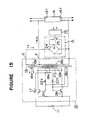
- FIG 15 is a circuit diagram showing the eighth embodiment of the lighting circuit according to the present invention.
- the output transformer for the inverter 15 is constructed with a leakage type transformer 18, and an auxiliary winding 18R wound in subtractive polarity at its secondary side is connected with the secondary windings 18S to form a low voltage cable way E.
- the switching device A same as that shown in Figure 3.
- the secondary winding 18S forms a high voltage cable way F, to which the fluorescent lamp 16 is connected.
- control device 19 is this eighth embodiment of the present invention is exactly same as that of Figure 4, with the exception that the power source winding 18d thereof is wound at the primary side. It should be noted also that the preheating circuit for the electrodes 16f, 16f in the lamp 16 is omitted from the illustration.
- the inverter 15 commences its oscillation in the same manner as that in Figure 3, and the control device 19 introduces into the transistor 25 an input signal same as that shown in Figure 5(c).
- the transistor 25 becomes conductive during the period To.
- the transformer 18 is of the leakage type, the voltage applied to the lamp 16 also assumes substantially zero volt.
- the transistor 25 is interrupted and a voltage in the vicinity of the maximum instantaneous value of the winding 18S is applied to the lamp 16, whereby it is lit.
- a diode of low voltage withstand and high speed response can be used for the transistor 25 and the rectification circuit 24, hence it becomes possible not only to construct the device with high reliability and at a reduced manufacturing cost, but also to further increase the general efficiency of the device.
- FIG 17 is a circuit diagram showing the nineth embodiment of the lighting circuit according to the present invention, in which the abovementioned point is improved.
- the control device 19, etc. are omitted from the illustration.
- the choking coil 33 as the current limiting impedance is added in series with the switching device A in the low voltage cable way shown in Figure 15.
- the current Is at the time of conduction of the switching device A can be reduced to thereby improve the abovementioned problem.
- the impedance value of the choking coil 33 is made too large, the voltage to be applied to the lamp 16 at the time of conduction of the switching device A becomes large.
- this voltage value becomes higher than a discharge maintaining voltage at the time of restriking of the lamp 16, the lamp commences its discharge before the switching device A is interrupted, and the rising in the voltage and the current for the lamp 16 are no longer steep, thereby hindering improvement in the lamp efficiency.
- the inverter 15 is of the self-excited type, as in the above-described embodiments, if a difference between the current Is and the current I L is too large, the oscillation of the inverter tends to become instable.
- the choking coil 33 has the effect of stabilizing the oscillation by reducing the current I 5 .
- Figure 18 is a circuit diagram showing the tenth embodiment of the lighting circuit according to the present invention. This embodiment performs the same operations as that shown in Figure 15 and attains the same effect, even if both low voltage cable way E and high voltage cable way F are individually provided at the secondary side of the transformer 18. In this case, the polarity of the windings 18S and 18R has no bearing on the operation of the transformer 18.
- Figure 19 is a diagram showing the eleventh embodiment of the lighting circuit according to the present invention, in which a tap T is provided at the intermediate point of the secondary winding 18S to form the low voltage cable way E.
- a reference numeral 46 designates a current transformer provided in the high voltage cable way F, the signal of which is input into the control device 19.
- FIG 20 is a circuit diagram showing details of the control device 19 for the eleventh embodiment, in which a starting auxiliary means C to be explained hereinbelow is added to the circuit shown in Figure 4.
- a reference numeral 47 designates a transistor connected in parallel with the capacitor 27 through the resistor 48
- a numeral 49 refers to a transistor arranged in parallel with the transistor 29
- a numeral 50 refers to a diode bridge which performs the full-wave rectification of the output signal from a current transformer 46
- a reference numeral 51 denotes a smoothing capacitor
- a numeral 52 indicates a base resistor of the transistor 47
- a reference numeral 53 designates a diode interposed between the collector of the transistor 49 and the base of the transistor 25.
- a capacitor 54 and a resistor 55 are connected in series between the positive polarity of the capacitor 27 and the base of the transistor 25 to thereby form a time constant circuit.
- the power source winding 18d of the control device 19 and the preheating winding 18f of the electrode 16f (not shown) is provided at the primary side of the transformer 18.
- the base current flows in the transistor 25 through the abovementioned time constant circuit.
- the transistor 47 since no signal has yet been generated in the current transformer 46, the transistor 47 is in an interrupted condition, hence there is no possibility of current flowing into the transistor 49 from the time constant circuit due to presence of the diode 53, even if the transistor is in a conductive state.
- the transistor 29 performs the same operations as that shown in Figure 4, its signal does not flow into the transistor.49 to be input into the transistor 25.
- the electrode 16f is preheated by the winding 18f.
- the switching device A continues its conductive state, substantially no voltage is applied to the lamp 16, hence it is not operated.
- the transistor 25 After lapse of a predetermined time instant t 1 , when the capacitor 54 is sufficiently charged and the base current of the transistor 25 is rendered substantially zero, the transistor 25 is brought to an interrupted state. However, since no signal is generated in the current transformer 46, the transistor 49 maintains its conductive state and the transistor 25 also maintains its interrupted state during a period of from t, to t 2 , on account of which a no-load voltage of the secondary winding 18S is applied, as it is, to the lamp 16.
- the electrode 16f is sufficiently preheated during a period of from to to t 1 , and still continues its preheating even during a period of from t 1 to t 2 . Therefore, a time interval is required more or less for the lamp 16 to shift from its glow discharge to its arc discharge, although this time period of from t 1 to t z is a relatively short time interval.
- the lamp 16 When the lamp 16 starts at a time instant t 2 , a signal is generated in the current transformer 46, and the transistor 47 becomes conductive. On account of this, the transistor 49 is interrupted and the signal generated in the transistor 29 is input into the transistor 25. As the result of this, the lamp 16 is operated with a voltage having its pause-time period of To and its voltage applying period of T ⁇ .
- the transistor 47 becomes conductive with a signal to be generated in the current transformer 46 when the lamp 16 is in its flow discharge condition during a period of from t, to t 2 , there is a possibility such that the lamp 16 remain in its glow discharge condition, or, if not remaining in this glow discharge condition, a time is taken for the lamp to shift from the glow discharge to the arc discharge, thereby shortening the service life of the lamp.
- an element such as, for example, a constant voltage diode, etc. which does not operate with a signal at the time of the glow discharge, but operate with a signal at the time of the arc discharge be provided in the base circuit of the transistor 47.
- the switching device A is constructed with a combination of the rectification circuit 24 and the transistor 25, although the same resulting effect can be obtained with those switching devices using other switching elements such as a field-effect transistor 25, and so on.
- the control device 19 varies its function by the switching element used, and there are contemplated various kinds of such switching elements other than those used in the above-described embodiments.
- the inverter 15 is a self-excited, constant current type push-pull transistor inverter. Besides this, there may also be used a serial inverter 15, for example, provided that the leakage type transformer 18 can be used as the output transformer, in which a substantially sinusoidal output voltage can be obtained.
- a smoothed d.c. voltage is used for the power source 11.
- Figure 22(a) indicates an output voltage V DB of the diode bridge 26 of the control device 19 and a Zener voltage V z of the constant voltage diode 31 of the same.
- Figure 22(b) shows an interrupted period Tl, of the transistor 25 in the switching device.
- Figure 22(c) shows an output current from the inverter 15. Due to presence of the choking coil 23, the output current from the inverter has its phase delayed from the output voltage from the inverter 15, i.e., the output voltage VD13 from the diode bridge 26. This output voltage V DB is clipped by the constant voltage diode 31 to form the period T i .
- Figure 23 is the circuit diagram showing the twelfth embodiment of the present invention, wherein the same reference numerals as those in Figure 3 designate the identical or equivalent parts. Further, Figure 24 illustrates one embodiment of the control device 19 for use in the device according to the twelfth embodiment of the present invention.
- a reference numeral 33 designates a current transformer which detects the output current from the inverter 15 and inputs the current into the control device 19.
- a numeral 33 refers to the same current transformer as mentioned above
- a reference numeral 34 designates an output resistor for the current transformer 33, 35 a full-wave rectifier to rectify the output from the current transformer 33, 31 a constant voltage diode, and 36 a d.c. power source for driving the device, which can be constructed by, for example, rectifying and smoothing an output from the auxiliary winding provided in the transformer 18 of the inverter 15.
- This circuit construction is substantially same as that shown in Figure-4 with the only differences in that the input signal for the constant voltage diode 31 is derived from the full-wave rectification of the output from the currenttransformer31, and that a signal reversing circuit consisting of a transistor 37 and a resistor 38 is added. Moreover, the graphical representation in Figure 22(d) indicates the output voltage from the current transformer 33, the output having a substantially same phase as, and analogous waveform to, those of the output current from the inverter 15, as a matter of course.
- the current transformer 33 does not produce an output voltage before the lamp 16 starts its electric discharge, and the transistor 25 maintains its interrupted conditions, on account of which the output voltage from the inverter 15 is applied to the lamp 16 as it is to facilitate commencement of its discharge.
- the current transformer 33 In the next place, when the lamp 16 starts its electric discharge, the current transformer 33 generates an output voltage.
- the transistor 29 becomes conductive during the period T 1a including the maximum instantaneous value of the output current from the inverter 15 by means of the constant voltage diode 31 as shown in Figure 22(d), to thereby interrupt the transistor 25.
- the discharge current flows through the lamp 16 during this period Tl,, as shown by the hatch-lined portion in Figure 22(c).
- the current flowing in the lamp 16 takes its waveform as shown in Figures 15(b) and 25(d) when no switching device A is provided.
- a level for detecting the output voltage from the current transformer 33 by means of the constant voltage diode 31 is set at a predetermined value A L as shown in Figures 25(b) and 25(d). Then, at a portion where the peak value is higher than the predetermined value A L , the control device performs the same operation as has been explained with reference to Figure 22, but, at a portion where the peak value is lower than the predetermined value A L , the switching device A maintains its interrupted condition.
- control device By constructing the control device as such, i.e., by providing the pause-time period for only a period where the maximum instantaneous value of the lamp current is greater than the predetermined value A., and by flowing a current having no pause-time period for a period where the instantaneous value of the lamp current is low, it is possible to further improve the operating efficiency of the lamp 16.
- the explanations have been given as to an example of using the current transformer 33 for the control device 19.
- the other expedients such as, for example, one which detects the current by use of resistors, etc. may be used.
- the constant voltage diode 31 is used for detection of the instantaneous value of the output current, which can also be replaced by a comparator IC, or the like for obtaining the same effect.
- the switching device A is constructed with combination of the rectifying circuit 24 and the transistor 25, which can also be replaced by a field-effect transistor or other switching elements for obtaining the same effect.
- the inverter 15 may be such one as, for example, a serial inverter, etc. provided that a substantially sinusoidal output voltage can be obtained at the output terminal thereof.
- the current limiting impedance 23 to set the lamp current at a predetermined value may not be inductance of the inductive reactance, but a capacitor of capacitive reactance. Further, in the foregoing, explanations have been given as to a case, wherein the choking coil is used at the output terminal of the inverter 15, although the transformer 18 of the inverter 15 may be constructed as the leakage transformer.
- the switching device A is possible other than that in the embodiment.
- an additional winding in the opposite polarity as that of the secondary winding 18S of the transformer 18 is provided, through which the switching device A is connected; or when the transformer 18 is the leakage type transformer, an intermediate tap is provided in the secondary winding and the switching device A is connected with a low voltage cable way to be formed in this intermediate tap; or it may be feasible that an impedance is connected in series with the switching device A to reduce the current flowing through the switching device A.
- the switching device A is connected in parallel with the lamp 16 through the electrodes 16f, 16f thereof, and the preheating current is caused to flow at the time of conduction of the switching device A.
- the voltage in the control winding 18d also varies in accordance with the input d.c. voltage of the inverter. Accordingly, when the input d.c. voltage of the inverter 15 is of a voltage waveform having large ripplies, i.e., if a difference between the maximum value (E max ) and the minimum value (E mln ) of the input d.c.
- the circuit in this fourteenth embodiment is so constructed that the stable control of the circuit can be effected with a voltage obtained by use of this type of inverter as the input signal for the control device, which does not vary so remarkably even when the ripples in the input d.c. voltage become fairly large.
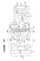
- Figure 27 illustrates the fourteenth embodiment of the lighting circuit according to the present invention
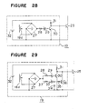
- Figure 28 shows a concrete embodiment of the control device therefor. It is to be noted that explanations will be made with reference to Figure 27 only for those parts which are different from those in the circuit of the Figure 3 embodiment.
- a reference numeral 14 designates an auxiliary d.c. power source having a peak value lower than the peak value of the output voltage from the smoothing capacitor or the rectifying circuit 13.
- the output transformer 18 contains therein the current limiting impedance constructed with a leakage type transformer.
- an impedance 26 in this embodiment, a choking coil
- This choking coil 26 is set at such an inductance value that no current may flow in the lamp 16 during a period when the switching device is in a conductive state.
- a reference numeral 18d represents a control winding; a numeral 28 refers to a resistor; 29 a constant voltage diode; 30 a transistor; 31 a resistor; and 32 a control d.c. power source, which can also be obtained by rectifying and smoothing an output from the control winding provided at the primary side of the output transformer 18.
- the input d.c. voltage for the inverter 15 is as shown in Figure 26(a).
- the inverter 15 carries out the self- oscillation to generate a high frequency voltage, thereby operating the lamp 16.
- the output transformer 18 is the leakage type transformer, wherein the control winding 18d wound around the magnetic circuit at the secondary side of this transformer generates a voltage analogous to the voltage from the secondary winding 18s, i.e., a voltage analogous to the voltage appearing across the terminals of the lamp 16.
- the impedance 26 functions to generate in the control winding 18d a voltage above the minimum required level when the switching device A becomes conductive.
- Figure 29 illustrates the fifteenth embodiment of the lighting circuit according to the present invention, in which the control device 19 is further provided with resistors 35, 37, a constant voltage diode 33, a capacitor 34, and a transistor 36.
- the transistor36 Before start of the electric discharge in the lamp 16, the transistor36 is rendered and maintained in a conductive state in utilization of the phenomenon that the voltage in the secondary winding 18s and the control winding 18d is higher during this period than at the time of operating of the lamp, thereby keeping the switching device in an interrupted state and facilitating start of the lamp.
- a choking coil is used as the impedance 26, although it goes without saying that a capacitor may also be used for the purpose. From the standpoint of obtaining a quick rising of the current to be supplied to the lamp 16, this latter component is preferred. In the case of using the choking coil, it may be connected to the output side of the full-wave rectifying circuit.
- the impedance 26 is connected in series with the switching device A to thereby generate a required voltage in the control winding 18d even when the switching device is in a conductive state.
- the winding provided in the magnetic circuit at the secondary side does not produce a voltage in the leakage transformer during conduction of the switching device.
- the following is an embodiment of the circuit which is applicable to such case.
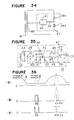
- FIG 30 shows the sixteenth embodiment of the lighting circuit according to the present invention, wherein the construction is the same as that shown in Figure 25 with the exception of the control device 19 (also no impedance 26 is provided).
- the point of difference in this embodiment from that shown in Figure 26 is that the capacitor 38 is connected with the output terminal of the control device 19.
- Figures 31(a), 31(b) and 31(c) are diagrams for explaining the operations of the circuit according to the sixteenth embodiment of the present invention, wherein the solid line in Figure 31(a) indicates an output current from the secondary winding 18s of the inverter, and a hatch-lined portion denotes the current flowing in the lamp 16; the solid line in Figure 31 (b) indicates an output voltage from the full-wave rectifying circuit 27 of the control device; and Figure 31(c) shows a voltage to be applied across the base and the emitter of the transistor 25.
- the method for generating this pause-time period To may be any one, other than that in the above-described embodiment, such as use of an appropriate timer, use of a monostable multi-vibrator, and others.
- the lighting circuit according to the sixteenth embodiment shown in Figure 30 be used in combination with a device as shown in Figure 29 for not generating the pause-time period at the time of starting the lamp.
- the switching device is connected in parallel with the lamp through its filament, the conduction period To of the switching device is extended (or the interruption period T 1 is omitted) at the time of starting the lamp so as to sufficiently preheat the filament, thereafter the conduction period To is shortened (or To may be omitted) to facilitate starting of the lamp discharge, and, after operating of the lamp, the conduction period To and the interruption period T 1 be set at their initial values.
- the self-excited, push-pull inverter is suited. Besides this, any type of inverter, which is capable of stopping the power supply to the lamp at least at the rising part of a substantially sinusoidal output current at every half cycle thereof, and of performing the power supply to the lamp in the vicinity of the maximum instantaneous value thereof.
- the output transformer may not necessarily be the leakage type transformer.
- a low d.c. voltage to be obtained by use of a transformer, etc., or such voltage generated from voltage dividing by the serial connection of a plurality of capacitors, and by other expedients.
- the d.c. voltage may contain therein the ripples, if only it is able to maintain the lamp discharge.
- the switching device A used is constructed with the rectifying circuit 24 and the transistor 25.
- this switching device may also be constructed with other switching elements, etc. having a required characteristic.
- other connection device may be adopted, if the power supply stoppage period to the lamp can be provided.
- the lamp 16 is operated by the circuit construction shown in Figure 23; however, when the electric discharge becomes difficult due to the service life of the lamp reaching its end, or no regular discharge can be done in any longer due to progress in consumption of one if the electrodes to bring about the asymmetrical discharge, etc., wherein the discharge is effected with only one of the polarities, there inevitably occurs the phenomenon to be mentioned in the following. That is to say, in case the switching device A is conductive during a period including the phase 8 0 in Figure 5(c) and this conductive state is interrupted at the phase 6 1 , there will be no problem at all so far as the current flows through the lamp 16.
- the choking coil 23 as the current limiting impedance is abruptly interrupted from its current flow to generate a high voltage due to the counter-electromotive force, which is applied to the switching device A.
- the output transformer 18 is constructed as the leakage transformer, and no choking coil 23 is used.
- the rising part of the current and voltage in the lamp 16 (a time instant t 1 or its vicinity shown in Figures 32(d) and 32(e)), when the lamp is operated with the lighting circuit according to the twelfth embodiment shown in Figure 23, can be shown in an enlarged waveform in these figures of drawing.
- a current increase exists in the lamp current, as shown by a broken line in Figure 32(d). This current increase varies in accordance with magnitude of impedance in the choking coil 23.
- the lamp voltage at its rising part t 1 is at a lower value V 1 than a value V 2 which can be anticipated from the locus of the original inverter output voltage, as shown in Figure 32(e), and it becomes substantially coincident with the locus of the original output voltage after the time instant t 2 .
- a time required for this time period between t 1 and t 2 is approximately 2 ⁇ s (more accurately, longer than 1.5 ps but not reaching 3 ps) with a fluorescent lamp of 40W capacity, for example. This phenomenon may be inferred due to the current flowing in the vicintiy of the tube wall of the lamp at the restriking thereof for every half cycle, though the detailed reasons therefor is yet to be clarified.
- the lighting circuit in this fifteenth embodiment of the present invention purports to effectively utilize the voltage dropping phenomenon to occur at the rising part of the lamp voltage as mentioned above, thereby reducing the voltage to be applied to the switching device.
- the embodiment will be explained in reference to the drawing.
- a reference numeral 37 designates a surge absorbing circuit
- a numeral 38 refers to a diode
- 39 and 40 refer to resistors
- 41 a capacitor.
- the remaining construction of the device according to this embodiment are the same as that shown in Figure 23, hence the corresponding parts are designated by the same reference numerals and the explanations for them are dispensed with.
- the surge absorbing circuit 37 in its normal operation, performs its charging operation to some extent at the rising part t 1 of the voltage at every half cycle of the lamp operation, although the main charging operation thereby is set to be in a constant which terminates within 3 ps. Accordingly, irrespective of presence of the surge absorbing circuit 37, the lamp 16 indicates its lamp voltage at a substantial equal level to that when no surge absorbing circuit is provided.
- the surge absorbing circuit 37 should contain therein at least a capacitor, a resistor serially connected with it, another resistor connected in parallel with it, and a diode. In this manner, the application of the high voltage to the switching device A can be prevented by means of the surge absorbing circuit.
- the surge absorbing circuit 37 may be constructed as in the above-described embodiment with respect to the secondary winding 18S; besides this, the circuit may be connected with the secondary winding through a middle point as shown in Figure 34, or it may be connected with another winding of the secondary winding which is further provided at the secondary side.
- connection of the surge absorbing circuit 37 in parallel with the switching device A as in the fifteenth embodiment shown in Figure 33 is effective not only in the case of connecting the inductive impedance in series with the switching device A (the device construction as shown in Figure 23), but also in the case of further connecting an auxiliary choking coil, etc. in parallel with the lamp and in series with the switching device A.
- the inverter may be of such a construction that it is able to generate a substantially sinusoidal output and to supply a high frequency power having a pause-time period to the lamp, and that the main impedance for limiting the lamp current in the inverter is constructed with the inductive reactance.
- the input d.c. voltage to the inverter may not necessarily be one which has been rectified and smoothed by the smoothing capacitor as in the foregoing embodiments, but it may be those such as pulsating current obtained without provision of the smoothing capacitor 14 or its equivalent component, or one obtained by using an appropriate auxilairy d.c. power source at this portion for the smoothing capacitor.
- the switching device A may utilize various switching elements such as, for example, a field-effect transistor, etc.
- the method for connecting the switching device A may be of variety when the output transformer is the leakage type transformer, though any type of the connecting method is possible, provided that a desired high frequency power can be supplied. It is further feasible to combine it with an expedient for properly controlling the switching device A and also performing starting and preheating operations of the lamp.
- the circuit of this twelfth embodiment has such an advantage that the instantaneous value A 1 of the lamp current when the current begins to flow in the lamp 16 remains to be a constant value irrespective of variations in the power source voltage, etc., although, on the other hand, the circuit is supposed to have an inconvenience to be mentioned as follows. That is to say, when it is considered that the input d.c. voltage of the inverter 15 contains many ripples, for example, when the voltage as shown in Figures 25(a) and 25(c) is generated in the inverter 15, the peak value of the lamp current is also high during a period wherein the peak value of the output voltage is high, and the period Tla (refer to Figure 22) during which the current flows through the lamp 16 becomes also long.
- Figure 35 illustrates the control device 19 for the lighting circuit for the electric discharge lamp as the nineteenth embodiment of the present invention, the control device being applicable to the lighting circuit such as, for example, shown in Figure 23.
- the control device as shown in Figure 35 is constructed with the current transformer 33, the resistor 34, the full-wave rectifying circuit 35, resistors 44, 45 for detecting and dividing voltage of the inverter output current at every half cycle, the diode 39, the capacitor 40, the resistor 41, the constant voltage diode 42, the resistor 43, the voltage comparator 46, the resistor 47, the auxiliary d.c. power source for driving 36, and the transistor 25 for the switching device A.
- the terminal voltage of the capacitor 40 assumes a voltage analogous to an envelope of the peak value of the output current from the inverter 15 or to the input d.c. voltage into the inverter 15.
- the voltage comparator 46 has its output transistor rendered conductive during a period of the voltage at the input terminal A becoming higher than the voltage at the input terminal B thereof, i.e., during the periods of D 1 and D 2 as shown in Figure 36(b), and the output terminal C assumes a low voltage level (as shown in Figure 36(c)). Accordingly, the transistor 25 becomes non-conductive during the periods 0 1 and D 2 , and the current flows to the side of the lamp 16.
- the period 0 1 during which the peak value is small and the period D 2 during which the peak value is large can be appropriately set by selection of a voltage dividing ratio of the resistors 44, 45 and a zener voltage in the constant voltage diode 42.
- the control of the device is effected in correspondence to the peak value of the output current from the inverter. It may however be feasible to effect the control in accordance with the input voltage for the inverter 15 by such means that, for example, a high frequency component is eliminated from the output voltage in the winding provided on the transformer 18 for the inverter 15, and the output voltage is rectified and applied to the input terminal B of the voltage comparator 46. It is also feasible that, in the state of the peak value of the output current from the inverter being lower than a predetermined value, as, for example, in the period during which the peak value is lower than the current value A L in Figures 25(b) and 25(d), the lamp current be so set that no pause-time period be provided therein.
- the current transformer 33 in the control device 19 has been taken as an example, although other expedient may of course, be adopted, such as, for example, detection of current by use of a resistor, etc. Furthermore, a period during which the current is supplied to the lamp is set by use of the voltage comparator 46, which may also be carried out by other expedients.
- the switching device A is a combination of the rectifying circuit 24 and the transistor 25, although the same effect can be obtained by use of the field-effect transistor, and other switching elements.
- the inverter 15 may be of any type that is able to obtain a substantially sinusoidal output voltage at its output terminal, such as, for example, a serial inverter or a bridge type inverter provided with an output transformer.
- the current limiting impedance 23 for setting the lamp current at a predetermined value may not only be the inductance of the inductive reactance, but also the capacitance of the capacitive reactance.
- the transformer 18 of the inverter 15 may also be constructed as the leakage type transformer.
- the arrangement of the switching device A is possible other than that shown in the above-described embodiment. That is to say, an additional winding having an opposite polarity to that of the secondary winding 18S of the transformer 18 is provided, by way of which the switching device A is connected, or, in the case of the transformer 18 being the leakage type transformer, an intermediate tap is provided on the secondary winding and the switching device A is connected with a low pressure cable way to be formed by this intermediate tap. Or, it may also be feasible that an impedance is connected in series with the switching device A to thereby reduce the current flowing in the switching device. Furthermore, it may be feasible that the switching device A is connected in parallel with the lamp 16 through the electrodes 16f, 16f and the preheating current is caused to flow through it at the time of its conduction.
- the input d.c. voltage for the inverter 15 may also be the pulsating d.c. voltage as shown in Figure 25(a), or the d.c. voltage as shown in Figure 25(c) which is not perfectly smoothed, but obtained from the circuit constructed in combination with an appropriate d.c. power source, and so forth.
- the period for supplying electric current to the lamp is maintained substantially constant irrespective of magnitude of the output current from the inverter or instantaneous variations in the input d.c. voltage for the inverter, thereby reducing variations in the power consumption in the lamp at every half cycle.
- control device 19 is constructed, in addition to the full-wave rectifier 35 and the d.c. power source 36, the resistors 39 and 40, a transistor 41 having an output terminal L, monostable multi-vibrators 42, 43, each having an output terminal M and N and generating an output for a predetermined time period, resistors 44, 45 and 46, capacitors 47 and 48, and a transistor 49, thereby performing the drive-control of the transistors 25 in the switching device A.
- Figures 38(a) to 38(f) respectively indicate signals corresponding to the output terminals K to 0 shown in Figure 37.
- Figure 38(f) shows the output current from the inverter 15, in which the hatch-lined portion designates the current flowing in the lamp 16. Assume now that the inverter 15 generates a high frequency voltage and the lamp 16 commences the electric discharge.
- the output current from the inverter 15 flows in either switching device A or the lamp 16, and voltage resulted from the full-wave rectification of the output voltage from the current transformer 33 is as shown in Figure 36(a).
- the transistor 41 is interrupted, and a synchronous signal as shown in Figure 38(b) is obtained at the output terminal L.
- the monostable multi-vibrators 42, 43 are of the type which is triggered by the trailing part (shown by an arrow in the drawing) of the input signal and performs the time limiting operation.
- the monostable multi-vibrators 42, 43 perform their predetermined time-limiting operation, whereby the output voltages as shown in Figures 38(c) and 38(d) are generated at their respective output terminals M and N. These voltages are reversed by the transistor 49, while the output from the output terminal O becomes as shown in Figure 38(e), to drive the transistor 25 of the switching device A, whereby the current in the hatch-lined portion of Figure 38(f) flows through the lamp 16. Since the period of this current flow is determined by the time-limiting operation of the monostable multi-vibrator 43, it can be maintained at a substantially constant level irrespective of the output current from the inverter 15.
- the synchronous signal is generated by use of the current transformer 33, there may be used any other means which is capable of operating the switching device A so that the current flowing in the lamp 16 may include therein the peak value and its vicinity of the output current from the inverter. 15, and of being operated for a substantially constant time period.
- the switching device A according to this embodiment is a combination of the rectifying circuit 24 and the transistor 25, the same effect can be obtained by use of a field-effect transistor, or other switching elements.
- the connection of the switching device A can be effected by other method than the above-described embodiment.
- an additional winding having the opposite polarity to that of the secondary winding 18S of the transformer is provided, by way of which the switching device A is connected, or, in the case of the transformer 18 being constructed as the leakage type transformer without use of the choking coil 23, an intermediate tap is provided in the secondary winding 18S and the switching device A is connected with a low pressure cable way to be formed by this intermediate tap, or other winding may be made the low voltage cable way.
- impedance in series with the switching device A so as to reduce the current flowing in the switching device A. It is moreover feasible that the switching device A is connected in parallel with the lamp 16 through the electrodes 16f, 16f and the preheating current is caused to flow at the time of its conduction.
- the input d.c. voltage for the inverter 15 may use a pulsating d.c. voltage as shown in Figure 25(a), or a d.c. voltage obtained from a circuit constructed in combination with an appropriate auxiliary power source of low peak value as shown in Figure 25(c).
- the switching device A is kept in the interrupted state with the cycle having its peak value lower than a certain current value A L as shown in Figure 25(d) by detecting the voltage level at the terminal K and controlling the transistor 49, and that the device of the present invention is operated with the cycle alone having the peak value higher than the current value AL.
- the switching device may be of a low voltage withstand.
- the inverter 15 is of such a type that generates a substantially sinusoidal output voltage at the output terminal thereof, and uses the capacitive or inductive reactance as the current limiting impedance to set the lamp current.
- a serial inverter or a bridge type inverter provided with the output transformer is also useful.
- This embodiment is of a such a construction that, when the lamp does not perform its normal electric discharge, the switching device connected in parallel with the lamp is conducted and maintained to thereby prevent application of the surge voltage to the switching device or generation of excessive inverter current.
- Figure 39 illustrates the construction of the lighting circuit according to the present embodiment, in which a point of difference from the fourteenth embodiment in Figure 27 resides in that no choking coil is provided.
- Figure 40 shows the construction of the control device 19 for use in the circuit of Figure 39, which comprises resistors 34, 37, 39 and 42, the constant voltage diode 35, the capacitors 33, 36, the thyrister 38, the diodes 40, 43, and the transistor 41.
- the voltage in the control winding 18d is as shown by a solid line in Figure 41.
- the transistor 30 becomes conductive, and, after a predetermined time to be decided by the resistor 31 and the capacitor 33, the transistor 25 is interrupted, whereby the output current in the inverter 15 flow through the lamp 16.
- the transistor 30 is interrupted, the transistor 25 becomes conductive, and the current does not flow through the lamp 16.
- the voltage in the control winding 18d becomes higher as shown by a dot line in Figure 41 than the voltage during its normal operation (shown by the solid line); in particular, in its asymmetrical discharging, the voltage increases from its normal voltage level at either positive or negative polarity in the waveform as shown in Figure 41.
- the output voltage from the full-wave rectifier 27 becomes higher than a set voltage V 35 in the constant voltage diode 35, the thyristor 38 becomes conductive and the transistor 41 is interrupted.
- the base current continues to flow in the transistor 25 through the resistor 42, and the transistor 25 maintains its conductive state, whereby a high voltage is no longer applied to the lamp 16.
- increase in current and voltage due to the asymmetrical discharging and generation of the high surge voltage at the time of non- lighting of the lamp are prevented.
- the capacitor 36 and the resistor 37 function to prevent the thyristor 38 from becoming conductive at the time of the operating of the lamp 16, either at the initial stage of its operating or until commencement of its operating.
- the switching device A when the thyristor 38 becomes once conductive, this conductive state is maintained; however, after lapse of a predetermined time period using a timer, etc., the switching device A may be reinstated to its interrupted state.
- the current to flow during maintenance of the switching device A in its conductive state may be set at a value which is not very much different from that during the operating of the lamp by setting the leakage inductance of the output leakage transformer 18 in the inverter 15; however, it is also feasible to provide the impedance 26 as has been done heretofore.
- the switching device A is connected in parallel with the lamp 16 through its filament; at the time of operating of the lamp, the conduction period of the switching device A is extended (or the interruption period T, may be eliminated) to sufficiently preheat the filament, thereafter, the period To is made shorter (or may be eliminated) to facilitate commencement of the electric discharge in the lamp 16; and after the operating, the periods To and T, are reinstated to their original set values.
- the voltage in the control winding 18d wound at the secondary side of the leakage type output transformer 18 as the input signal into the control device 19.
- This object can be achieved by use of a voltage substantially analogous to the voltage across the lamp 16: for example, a signal generating transformer is connected in parallel with the lamp 16, and the voltage in the winding provided on this transformer is used as the input signal into the control device 19, in which case there may also be used a construction wherein the impedance 26 is connected.
- this phase difference may be compensated to subject the switching device A to the open and close controls. This can be realized, in the case of the leakage type transformer as in this embodiment, by appropriate adjustment of the winding position of the control winding 18d.
- the switching device A is operated by the voltage in the control winding 18d for both its normal and abnormal operations.
- the normal operation is performed by, for example, detecting the current flowing in the inverter 15 or the lamp 16 to provide an appropriate pause-time period, and, at the abnormal operation, the switching device A is operated by obtaining a voltage substantially analogous to the voltage across the terminals of the lamp 16 as in this embodiment.
- other means be provided to cause the switching device to perform the operations in conformity to its normal operations and its abnormal operations by detection of the current flowing through the lamp 16 or of the output current from the inverter 15.
- the self-oscillating push-pull inverter as used in this embodiment is suitable. Besides this, however, other types of the inverter may be used, which is capable of stopping the power supply to the lamp 16 at the rising part of a substantially sinusoidal output current at every half cycle thereof, and of supplying the power to the lamp at the maximum instantaneous value of the current or in its vicinity.
- the output transformer 18 may also not necessarily be of the leakage type. It is of course possible that, depending on the kind of the current limiting impedance of the lamp 16, when the impedance 26 connected in series with the switching device A is to be provided, the transformer may be constructed with a capacitor. From the standpoint of quicken the trailing of the current to be supplied to the lamp 16, the latter is preferable. Furthermore, when the choking coil is used as the impedance 26, it may be connected with the output side of the full-wave rectifying circuit 24.
- auxiliary d.c. power source 14 to the inverter 15 there may be used a low d.c. voltage to be obtained by use of a transformer, etc., besides a well known smoothing circuit, or a d.c. voltage generated from a divided voltage due to the series connection of a plurality of capacitors, or other means.
- the power source may contain therein the ripples, if only the required electric discharge of the lamp 16 can be maintained.
- the switching device A is constructed with the rectifying circuit 24 and the transistor 25. However, it may be made up of other switching elements having the required characteristic.
- the connection of the switching device A can be done by other methods than the above-described one, provided that a power supply stoppage period to the lamp 16 can be provided.
Landscapes
- Circuit Arrangements For Discharge Lamps (AREA)
Claims (22)
Applications Claiming Priority (16)
| Application Number | Priority Date | Filing Date | Title |
|---|---|---|---|
| JP41806/83 | 1983-03-14 | ||
| JP58041806A JPS59167999A (ja) | 1983-03-14 | 1983-03-14 | 放電灯点灯装置 |
| JP6634983A JPS59191295A (ja) | 1983-04-15 | 1983-04-15 | 高周波点灯装置 |
| JP66349/83 | 1983-04-15 | ||
| JP11785283A JPS6010595A (ja) | 1983-06-29 | 1983-06-29 | 放電灯点灯装置 |
| JP117852/83 | 1983-06-29 | ||
| JP14930283A JPS6041798A (ja) | 1983-08-16 | 1983-08-16 | 放電灯点灯装置 |
| JP149302/83 | 1983-08-16 | ||
| JP2271/84 | 1984-01-10 | ||
| JP2272/84 | 1984-01-10 | ||
| JP227184A JPS60146496A (ja) | 1984-01-10 | 1984-01-10 | 放電灯点灯装置 |
| JP2269/84 | 1984-01-10 | ||
| JP2270/84 | 1984-01-10 | ||
| JP227084A JPS60146495A (ja) | 1984-01-10 | 1984-01-10 | 放電灯点灯装置 |
| JP226984A JPS60146494A (ja) | 1984-01-10 | 1984-01-10 | 放電灯点灯装置 |
| JP227284A JPS60146497A (ja) | 1984-01-10 | 1984-01-10 | 放電灯点灯装置 |
Publications (2)
| Publication Number | Publication Date |
|---|---|
| EP0119584A1 EP0119584A1 (fr) | 1984-09-26 |
| EP0119584B1 true EP0119584B1 (fr) | 1989-01-18 |
Family
ID=27571462
Family Applications (1)
| Application Number | Title | Priority Date | Filing Date |
|---|---|---|---|
| EP19840102738 Expired EP0119584B1 (fr) | 1983-03-14 | 1984-03-13 | Circuit d'allumage pour lampe à décharge électrique |
Country Status (2)
| Country | Link |
|---|---|
| EP (1) | EP0119584B1 (fr) |
| DE (1) | DE3476315D1 (fr) |
Families Citing this family (2)
| Publication number | Priority date | Publication date | Assignee | Title |
|---|---|---|---|---|
| WO1998038840A1 (fr) * | 1997-02-28 | 1998-09-03 | Toshiba Lighting & Technology Corporation | Materiel d'eclairage et systeme d'eclairage a lampe a decharge |
| US6107751A (en) * | 1998-12-01 | 2000-08-22 | Billings; Keith | Current fed, parallel resonant ballast |
Family Cites Families (2)
| Publication number | Priority date | Publication date | Assignee | Title |
|---|---|---|---|---|
| US4087722A (en) * | 1975-05-01 | 1978-05-02 | American Ionetics, Inc. | Apparatus and method for supplying power to gas discharge lamp systems |
| US4350935A (en) * | 1980-03-28 | 1982-09-21 | Lutron Electronics Co., Inc. | Gas discharge lamp control |
-
1984
- 1984-03-13 EP EP19840102738 patent/EP0119584B1/fr not_active Expired
- 1984-03-13 DE DE8484102738T patent/DE3476315D1/de not_active Expired
Also Published As
| Publication number | Publication date |
|---|---|
| EP0119584A1 (fr) | 1984-09-26 |
| DE3476315D1 (en) | 1989-02-23 |
Similar Documents
| Publication | Publication Date | Title |
|---|---|---|
| US4734624A (en) | Discharge lamp driving circuit | |
| US5977725A (en) | Resonance type power converter unit, lighting apparatus for illumination using the same and method for control of the converter unit and lighting apparatus | |
| KR0137181B1 (ko) | 방전램프 점등장치 | |
| US4544862A (en) | Lighting circuit for electric discharge lamp | |
| JPS61198595A (ja) | ガス放電管内ア−ク放電防止装置 | |
| JP3271042B2 (ja) | 圧電トランスを用いた電圧変換装置 | |
| EP0477587A1 (fr) | Appareil d'alimentation | |
| EP0119584A1 (fr) | Circuit d'allumage pour lampe à décharge électrique | |
| US4961029A (en) | Discharge lamp lighting device | |
| JP2001211658A (ja) | 相補形スイッチを有するハロゲン電力変換器 | |
| JPH11144860A (ja) | 高周波加熱装置 | |
| JP3272218B2 (ja) | 照明装置 | |
| JP3400592B2 (ja) | 電源装置 | |
| JPS59180999A (ja) | 放電灯点灯装置 | |
| KR950004807Y1 (ko) | 전자식 형광등용 안정기 | |
| JP2520280B2 (ja) | 放電灯点灯装置 | |
| KR940002674Y1 (ko) | 전자식 형광등용 안정기 회로 | |
| KR200308322Y1 (ko) | 전자식 형광등용 안정기 | |
| KR100493922B1 (ko) | 전자식 형광등용 안정기 | |
| JPH0731155A (ja) | インバータ装置 | |
| JPH0351277B2 (fr) | ||
| JP3704754B2 (ja) | 放電灯点灯装置 | |
| KR200177679Y1 (ko) | 형광등용 전자식 안정기 | |
| JPH063757B2 (ja) | 放電灯点灯装置 | |
| JPH1187050A (ja) | 高周波加熱装置 |
Legal Events
| Date | Code | Title | Description |
|---|---|---|---|
| PUAI | Public reference made under article 153(3) epc to a published international application that has entered the european phase |
Free format text: ORIGINAL CODE: 0009012 |
|
| AK | Designated contracting states |
Designated state(s): DE FR GB NL |
|
| 17P | Request for examination filed |
Effective date: 19841106 |
|
| 17Q | First examination report despatched |
Effective date: 19860905 |
|
| GRAA | (expected) grant |
Free format text: ORIGINAL CODE: 0009210 |
|
| AK | Designated contracting states |
Kind code of ref document: B1 Designated state(s): DE FR GB NL |
|
| REF | Corresponds to: |
Ref document number: 3476315 Country of ref document: DE Date of ref document: 19890223 |
|
| ET | Fr: translation filed | ||
| PLBE | No opposition filed within time limit |
Free format text: ORIGINAL CODE: 0009261 |
|
| STAA | Information on the status of an ep patent application or granted ep patent |
Free format text: STATUS: NO OPPOSITION FILED WITHIN TIME LIMIT |
|
| 26N | No opposition filed | ||
| REG | Reference to a national code |
Ref country code: GB Ref legal event code: 746 Effective date: 19960611 |
|
| REG | Reference to a national code |
Ref country code: FR Ref legal event code: D6 |
|
| PGFP | Annual fee paid to national office [announced via postgrant information from national office to epo] |
Ref country code: GB Payment date: 19980304 Year of fee payment: 15 |
|
| PGFP | Annual fee paid to national office [announced via postgrant information from national office to epo] |
Ref country code: FR Payment date: 19980310 Year of fee payment: 15 |
|
| PGFP | Annual fee paid to national office [announced via postgrant information from national office to epo] |
Ref country code: DE Payment date: 19980320 Year of fee payment: 15 |
|
| PGFP | Annual fee paid to national office [announced via postgrant information from national office to epo] |
Ref country code: NL Payment date: 19980326 Year of fee payment: 15 |
|
| PG25 | Lapsed in a contracting state [announced via postgrant information from national office to epo] |
Ref country code: GB Free format text: LAPSE BECAUSE OF NON-PAYMENT OF DUE FEES Effective date: 19990313 |
|
| PG25 | Lapsed in a contracting state [announced via postgrant information from national office to epo] |
Ref country code: NL Free format text: LAPSE BECAUSE OF NON-PAYMENT OF DUE FEES Effective date: 19991001 |
|
| GBPC | Gb: european patent ceased through non-payment of renewal fee |
Effective date: 19990313 |
|
| PG25 | Lapsed in a contracting state [announced via postgrant information from national office to epo] |
Ref country code: FR Free format text: LAPSE BECAUSE OF NON-PAYMENT OF DUE FEES Effective date: 19991130 |
|
| NLV4 | Nl: lapsed or anulled due to non-payment of the annual fee |
Effective date: 19991001 |
|
| REG | Reference to a national code |
Ref country code: FR Ref legal event code: ST |
|
| PG25 | Lapsed in a contracting state [announced via postgrant information from national office to epo] |
Ref country code: DE Free format text: LAPSE BECAUSE OF NON-PAYMENT OF DUE FEES Effective date: 20000101 |