EP0120732B1 - Verfahren zur sequentiellen Steuerung einer Flüssigkristall-Matrixanzeigeeinrichtung unter Benutzung des cholesterisch-nematischen Phasenübergangs - Google Patents
Verfahren zur sequentiellen Steuerung einer Flüssigkristall-Matrixanzeigeeinrichtung unter Benutzung des cholesterisch-nematischen Phasenübergangs Download PDFInfo
- Publication number
- EP0120732B1 EP0120732B1 EP84400320A EP84400320A EP0120732B1 EP 0120732 B1 EP0120732 B1 EP 0120732B1 EP 84400320 A EP84400320 A EP 84400320A EP 84400320 A EP84400320 A EP 84400320A EP 0120732 B1 EP0120732 B1 EP 0120732B1
- Authority
- EP
- European Patent Office
- Prior art keywords
- potential
- liquid crystal
- threshold voltage
- time
- column
- Prior art date
- Legal status (The legal status is an assumption and is not a legal conclusion. Google has not performed a legal analysis and makes no representation as to the accuracy of the status listed.)
- Expired
Links
- 239000004973 liquid crystal related substance Substances 0.000 title claims description 62
- 238000000034 method Methods 0.000 title claims description 21
- 239000011159 matrix material Substances 0.000 title claims description 19
- 230000000694 effects Effects 0.000 title claims description 7
- 230000008859 change Effects 0.000 title description 7
- 230000001747 exhibiting effect Effects 0.000 title 1
- 230000007704 transition Effects 0.000 claims description 16
- 230000008569 process Effects 0.000 claims description 10
- 238000003384 imaging method Methods 0.000 claims 1
- 230000006870 function Effects 0.000 description 14
- PEDCQBHIVMGVHV-UHFFFAOYSA-N Glycerine Chemical compound OCC(O)CO PEDCQBHIVMGVHV-UHFFFAOYSA-N 0.000 description 8
- 230000003098 cholesteric effect Effects 0.000 description 8
- 239000013078 crystal Substances 0.000 description 6
- 230000005284 excitation Effects 0.000 description 6
- 210000004027 cell Anatomy 0.000 description 5
- 230000004044 response Effects 0.000 description 5
- 206010070834 Sensitisation Diseases 0.000 description 4
- 239000000975 dye Substances 0.000 description 4
- 238000012423 maintenance Methods 0.000 description 4
- 230000008313 sensitization Effects 0.000 description 4
- 241001080024 Telles Species 0.000 description 2
- ZUOUZKKEUPVFJK-UHFFFAOYSA-N diphenyl Chemical compound C1=CC=CC=C1C1=CC=CC=C1 ZUOUZKKEUPVFJK-UHFFFAOYSA-N 0.000 description 2
- 230000005684 electric field Effects 0.000 description 2
- 239000007788 liquid Substances 0.000 description 2
- 230000003446 memory effect Effects 0.000 description 2
- 239000000203 mixture Substances 0.000 description 2
- 230000004048 modification Effects 0.000 description 2
- 238000012986 modification Methods 0.000 description 2
- 230000000630 rising effect Effects 0.000 description 2
- 230000001235 sensitizing effect Effects 0.000 description 2
- 241001644893 Entandrophragma utile Species 0.000 description 1
- 239000002262 Schiff base Substances 0.000 description 1
- 150000004753 Schiff bases Chemical class 0.000 description 1
- 235000010290 biphenyl Nutrition 0.000 description 1
- 239000004305 biphenyl Substances 0.000 description 1
- 230000036755 cellular response Effects 0.000 description 1
- 210000002858 crystal cell Anatomy 0.000 description 1
- IGARGHRYKHJQSM-UHFFFAOYSA-N cyclohexylbenzene Chemical class C1CCCCC1C1=CC=CC=C1 IGARGHRYKHJQSM-UHFFFAOYSA-N 0.000 description 1
- 230000003247 decreasing effect Effects 0.000 description 1
- 230000001419 dependent effect Effects 0.000 description 1
- 150000002148 esters Chemical class 0.000 description 1
- 239000011810 insulating material Substances 0.000 description 1
- 230000003287 optical effect Effects 0.000 description 1
- 230000009467 reduction Effects 0.000 description 1
Images

Classifications
-
- G—PHYSICS
- G09—EDUCATION; CRYPTOGRAPHY; DISPLAY; ADVERTISING; SEALS
- G09G—ARRANGEMENTS OR CIRCUITS FOR CONTROL OF INDICATING DEVICES USING STATIC MEANS TO PRESENT VARIABLE INFORMATION
- G09G3/00—Control arrangements or circuits, of interest only in connection with visual indicators other than cathode-ray tubes
- G09G3/20—Control arrangements or circuits, of interest only in connection with visual indicators other than cathode-ray tubes for presentation of an assembly of a number of characters, e.g. a page, by composing the assembly by combination of individual elements arranged in a matrix no fixed position being assigned to or needed to be assigned to the individual characters or partial characters
- G09G3/34—Control arrangements or circuits, of interest only in connection with visual indicators other than cathode-ray tubes for presentation of an assembly of a number of characters, e.g. a page, by composing the assembly by combination of individual elements arranged in a matrix no fixed position being assigned to or needed to be assigned to the individual characters or partial characters by control of light from an independent source
- G09G3/36—Control arrangements or circuits, of interest only in connection with visual indicators other than cathode-ray tubes for presentation of an assembly of a number of characters, e.g. a page, by composing the assembly by combination of individual elements arranged in a matrix no fixed position being assigned to or needed to be assigned to the individual characters or partial characters by control of light from an independent source using liquid crystals
- G09G3/3611—Control of matrices with row and column drivers
- G09G3/3622—Control of matrices with row and column drivers using a passive matrix
- G09G3/3629—Control of matrices with row and column drivers using a passive matrix using liquid crystals having memory effects, e.g. ferroelectric liquid crystals
-
- G—PHYSICS
- G09—EDUCATION; CRYPTOGRAPHY; DISPLAY; ADVERTISING; SEALS
- G09G—ARRANGEMENTS OR CIRCUITS FOR CONTROL OF INDICATING DEVICES USING STATIC MEANS TO PRESENT VARIABLE INFORMATION
- G09G2300/00—Aspects of the constitution of display devices
- G09G2300/04—Structural and physical details of display devices
- G09G2300/0469—Details of the physics of pixel operation
- G09G2300/0478—Details of the physics of pixel operation related to liquid crystal pixels
- G09G2300/0482—Use of memory effects in nematic liquid crystals
- G09G2300/0486—Cholesteric liquid crystals, including chiral-nematic liquid crystals, with transitions between focal conic, planar, and homeotropic states
-
- G—PHYSICS
- G09—EDUCATION; CRYPTOGRAPHY; DISPLAY; ADVERTISING; SEALS
- G09G—ARRANGEMENTS OR CIRCUITS FOR CONTROL OF INDICATING DEVICES USING STATIC MEANS TO PRESENT VARIABLE INFORMATION
- G09G2310/00—Command of the display device
- G09G2310/06—Details of flat display driving waveforms
-
- G—PHYSICS
- G09—EDUCATION; CRYPTOGRAPHY; DISPLAY; ADVERTISING; SEALS
- G09G—ARRANGEMENTS OR CIRCUITS FOR CONTROL OF INDICATING DEVICES USING STATIC MEANS TO PRESENT VARIABLE INFORMATION
- G09G2310/00—Command of the display device
- G09G2310/06—Details of flat display driving waveforms
- G09G2310/061—Details of flat display driving waveforms for resetting or blanking
Definitions
- the present invention relates to a method for sequential control of a matrix imager using the cholesteric-nematic phase transition effect of a liquid cirstal. It finds an application in the production of liquid crystal display devices used in particular in the binary display of complex images or in the display of alphanumeric characters.
- the invention relates to the control of a matrix imager comprising a display cell constituted by two transparent insulating walls and by a liquid crystal comprising zones distributed in a matrix and interspersed in a system known as crossed bands or in English terminology in a “cross bar” system.
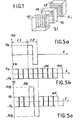
- FIG. 1 there is shown such a matrix imager.
- This comprises a display cell which has two walls 10 and 12, generally transparent, arranged on either side of a shim 14 of thickness, made of insulating material, defining a volume 16 which is occupied, when the cell is mounted, by a liquid crystal film.
- On the walls 10 and 12 are deposited two systems of electrodes each constituted by a series of parallel semi-transparent conductive strips; the rows of electrodes for example the number of p are denoted x ;, where i is an integer which can take all the values between 1 and p, and the columns of electrodes, for example the number of a are denoted y j , where j is an integer which can take all values between 1 and g.
- the useful surface of the liquid crystal is thus broken down into a mosaic of zones corresponding to the overlapping zones of the two electrode systems, each zone corresponding to the overlapping of two strips x i and y j and which can therefore be identified by the notation x i y j .
- the rows and columns of electrodes are capable of conveying electrical signals suitable for the excitation of the liquid crystal which has an optical property dependent on this excitation.
- the sensitization of an area of the liquid crystal is carried out by applying to the electrodes x; and y i electrical voltages which cause the appearance of an electric field within the liquid crystal.
- This electric field acts on the cholesteric-nematic phase transition of the liquid crystal.
- the liquid crystal has two threshold voltages, a low threshold voltage V B and a high threshold voltage V H such that 0 ⁇ V B ⁇ V H.
- the application of a potential difference between the lines x i and the columns y j , or control voltage, which is greater than the high threshold voltage V H makes it possible to obtain the liquid crystal in the nematic form and l application of a potential difference between the lines x i and the columns y j , which is less than the low threshold voltage V B , makes it possible to obtain the liquid crystal in the cholesteric form and this, whatever the phase previous liquid crystal.
- nematic phase for an area x i y j of the liquid crystal corresponds to the display of this area, the latter becoming white in the presence of a dichroic dye, and obtaining the cholesteric phase for this same zone corresponds to the non-displayed state of said zone, the latter then appearing black due to the dichroism of the dye.
- this type of display cell has a certain memory effect. Indeed, after having obtained the displayed state of the zone x i y j , the application of a potential difference between the line x i and the column y j between the voltages V B and V H is sufficient to maintain l displayed state of this zone. Similarly, after having obtained the not displayed state of the area x i y j , the application of a potential difference between the row x i and the column y (between the voltages V B and V H ) is sufficient to maintain the non-displayed state of said zone.
- these holding voltages from the displayed or not displayed state, are necessary to keep a good contrast between the displayed zones, or white dots and the non-displayed zones, or black dots; the absence of these holding voltages results in a significant reduction in said contrast.
- FIG. 2a the potential difference between the line x i and the column y i , or control voltage V c , has been represented as a function of time and in FIG. 2b the response curve of the liquid crystal as a function of the value of the potential difference V c , this response curve corresponding to the light intensity (I) transmitted by the area x i y j as a function of time.
- the steps 20 and 22 of the cell response curve correspond to the non-displayed state of the area x i y j ; the level 24 of this same curve corresponds to the displayed state of said zone and the rising and falling parts respectively 26 and 28 of said curve correspond to the cholesteric-nematic and nematic-cholesteric phase change respectively of the liquid crystal and therefore to the passage of the state not displayed in the displayed state and vice versa.
- the sensitization of the zone x i y j of the liquid crystal is carried out by sending to the line x i , for a time t 1 equal to r ⁇ , where r is an integer and ⁇ an elementary interval of time useful for the command, an electrical erasure signal, of amplitude much greater than the high threshold voltage V H of the liquid crystal followed by an electrical signal for addressing said line, for a time t 2 equal to ⁇ .
- the integer r depends on the speed of transition between its two phases of the liquid crystal used. Its value is a few general units ment 1, 2 or 3.
- the time r in fact corresponds to the minimum time necessary for the change of nematic-cholesteric phase of the liquid crystal (passage from the nematic phase to the cholesteric phase).
- an electrical addressing signal is applied to column y j , in particular an alternating signal with zero mean value having an effective value generally equal to that of the addressing signal of line x i , this signal being during time addressing t 2 of line x i either in phase or in phase opposition, with the addressing signal of said line.
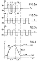
- FIGS. 3b and 3c show, as a function of time, the addressing signal of the column y j , respectively, in phase and in phase opposition with the addressing signal of the line x i , V b corresponding to the RMS voltage of said signals.
- the p lines are controlled successively and the g columns simultaneously in order to cause an image, or an alpha-numeric character, defined point by point, to appear on said imager.
- the response curves of the zone x i y j of the liquid crystal have been represented as a function of the previous sensitizations. These curves give the light intensity transmitted (I) by the liquid crystal zone as a function of time.
- the rising part 30 of the two curves O and P corresponds to the change of cholesteric-nematic phase of the liquid crystal (passage from the cholesteric phase to the nematic phase), this phase change taking place during the erasure period t l . It should be noted that the time to obtain this phase transition being relatively long, it is necessary to carry out the latter during the erasing period t 1 of the line x i .
- the level 32 of the curve 0 corresponds to the displayed state of the area x i y j , obtained when the signals applied to the line x i and the column y j are in phase opposition
- the level 34 of the curve P corresponds to the non-displayed state of the zone x i y j , obtained when phase x signals are applied to the line x i and the column y j
- the descending part 34a of the curve P corresponds to the change in nematic-cholesteric phase of the liquid crystal.
- the subject of the present invention is precisely a method of sequential control of a matrix imager using the cholesteric-nematic phase transition effect of a liquid crystal making it possible in particular to suppress the movement of such a white line on said imager.
- the awareness of a zone x i y j is done by reversing the role of the rows and columns of electrodes, which allows, when sensitizing the p zones of the liquid crystal of the same column y j , by applying the potential V 3 simultaneously on the p rows of electrodes , to suppress the scrolling of the white line on the imager.
- the sum V 4 + V5 is greater than the high threshold voltage V H to refresh during the scanning of the line the displayed state.
- the potentials V 2 and V 3 are equal.
- the different potentials V 1 , V 2 , V 3 , V 4 and V 5 are alternating potentials with zero mean values, V 1 , V 2 , V 3 , V 4 and V5 then representing the effective values of these potentials.
- a first potential V 1 is applied to the column y j (FIG. 1). a voltage much higher than the high threshold voltage V H of the liquid crystal.
- This first potential corresponds to the erasure signal relating to the area x i y j .
- This erasure signal is applied, as for the prior art, before the actual addressing of the zone x i y j , in order to allow the passage from the cholesteric phase to the nematic phase of the liquid crystal.
- This signal is applied for a time t 1 1 equal to s ⁇ , s being an integer which depends on the speed of transition between its two phases of the liquid crystal used and ⁇ the minimum time necessary for the transition from the nematic phase to the cholesteric phase.
- this erasure signal is an alternating signal with zero mean value, for example a rectangular signal, for which V 1 represents the effective value of said signal.
- This signal is in particular that which is represented on part 29 of the signal of FIG. 3a.
- a second potential V 2 is applied to said column y i corresponding to the address signal of the column.
- This addressing signal is applied for a time t 2 equal to ⁇ .
- this addressing signal of column y j is an alternating signal with zero mean value, for example a rectangular signal, for which V 2 represents the effective value of said signal.
- This signal is in particular that which is represented on the part 31 of the signal of FIG. 3a.
- a third potential V 3 corresponding to the line addressing signal is preferably an alternating signal with zero mean value, for example a rectangular signal, for which V 3 represents the effective value of said signal.
- This signal is in particular that shown in FIG. 3b or in FIG. 3c.
- the sum of the potentials V 2 + V 3 at the terminals of the liquid crystal, or control voltage, during the time t 2 for addressing the column y j must have a value greater than the high threshold voltage V H of the liquid crystal to obtain the displayed state of the area x i y j , in other words a white point on the imager.
- the potential difference V Z- V 3 during time t 2 , must have a value lower than the low threshold voltage V B of the liquid crystal in order to obtain the non-displayed state of the zone x i y j , in other words a black dot on the imager.
- the two potentials V 2 and V 3 are equal.
- obtaining the non-displayed state is done by using, during time t 2 , row and column signals in phase, such as those represented in FIGS. 3a and 3b.
- V 2 and V 3 equal to the value V o
- V 2 -V 3 a potential difference V 2 -V 3 equal to 0 is obtained.
- the columns of the imager not selected are brought to a zero continuous potential, for example the potential of the mass.
- the columns are controlled successively while the rows are controlled simultaneously. Furthermore, the display or not of an entire column of the imager is done by sensitizing, as described above, the p zones of said column by simultaneously applying to each line the potential V 3 .
- liquid crystals with a cholesteric-nematic phase transition exhibit a memory effect, that is to say that after having deleted the electrical control signal, the displayed or white points of the imager remain displayed. It is the same for the not displayed or black points.
- the contrast of these points decreasing over time, it is therefore necessary to maintain a certain voltage across the terminals of the corresponding zone x i y j to avoid too great a loss of contrast.
- a zero potential is applied to the line x i , for the time t 1 , that is to say without an erasure signal, and during time t 2 a fourth potential V 4 corresponding to the line addressing signal. Furthermore, a fifth potential V5 is applied to the column y corresponding to the column addressing signal.
- the row and column addressing signals are alternating signals with zero mean value, for example rectangular, for which V 4 and V5 respectively represent the effective values of said signals.
- the addressing signal of the line x i is represented , as a function of time, Va corresponding to the effective voltage of said row signal
- the addressing signal of the column y i is represented , as a function of time, V b corresponding to the RMS voltage of the column signal.
- the sum of the potentials V 4 + V5 at the terminals of the liquid crystal, during the addressing time t 2 must have a value greater than the low threshold voltage V B of the liquid crystal to maintain the displayed state of the area x i y j (white point).
- the potential difference V 4 -V5, during time t 2 must have a value lower than the high threshold voltage V H of the liquid crystal in order to maintain the non-displayed state of the zone x i y j (point black).
- the sum of the potentials V 4 + V5, for maintaining the displayed state is greater than the high threshold voltage V H of the liquid crystal. This improves the contrast between the zones in the displayed state (white dots) and the zones in the non-displayed state (black dots).
- the potential V 4 is chosen so as to be equal to twice the potential V5 to avoid any change in appearance during the scanning of the line.
- FIG. 5c the voltage V c applied to the terminals of the liquid crystal is shown, the signal 38, in solid line being obtained when the row and column signals are in phase opposition.
- the maintenance of the non-displayed state is done by using, for the time t 2 , row and column signals in phase, like the signal in FIG. 5a and the signal 40, in dotted lines, of Figure 5b.
- a potential V5 equal to V o a potential difference V 4 -V5 is obtained, or control voltage V, equal to V o , V o being chosen so as to be less than the high threshold voltage V H of the crystal liquid.
- the signal 42 in dotted lines, in FIG. 5c, represents the voltage V c applied to the terminals of the crystal, when the row and column signals are in phase.
- the lines are controlled successively. Furthermore the maintenance of the state displayed or not displayed of a whole line of the matrix imager, that is to say q zones of said line, is done by applying simultaneously to each column the potential V5.
- the values of the threshold voltages are of the order of a few volts. Typically, the low threshold voltage V B is equal to 5V and the high threshold voltage V H is equal to 10V.
- the liquid crystals used having a cholesteric-nematic phase transition, consist of a mixture of three components: a nematic component, a cholesteric component and a dye.
- nematic components such as components E7 and E43 from the company MERCK, esters, Schiff bases and phenylcyclohexanes.
- the cholesteric component can in particular be a mixture of CB15 produced by the company B.d.h and ZL811 produced by the company MERCK in proportions such that the pitch varies little with temperature.
- anthraquinons such as components D5 and D16 from the company B.d.h are dyes commonly used by those skilled in the art.
Landscapes
- Engineering & Computer Science (AREA)
- Chemical & Material Sciences (AREA)
- Crystallography & Structural Chemistry (AREA)
- Physics & Mathematics (AREA)
- Computer Hardware Design (AREA)
- General Physics & Mathematics (AREA)
- Theoretical Computer Science (AREA)
- Liquid Crystal (AREA)
- Liquid Crystal Display Device Control (AREA)
Claims (9)
Applications Claiming Priority (2)
| Application Number | Priority Date | Filing Date | Title |
|---|---|---|---|
| FR8303047 | 1983-02-24 | ||
| FR8303047A FR2541807B1 (fr) | 1983-02-24 | 1983-02-24 | Procede de commande sequentielle d'un imageur matriciel utilisant l'effet de transition de phase cholesterique-nematique d'un cristal liquide |
Publications (2)
| Publication Number | Publication Date |
|---|---|
| EP0120732A1 EP0120732A1 (de) | 1984-10-03 |
| EP0120732B1 true EP0120732B1 (de) | 1987-06-03 |
Family
ID=9286230
Family Applications (1)
| Application Number | Title | Priority Date | Filing Date |
|---|---|---|---|
| EP84400320A Expired EP0120732B1 (de) | 1983-02-24 | 1984-02-16 | Verfahren zur sequentiellen Steuerung einer Flüssigkristall-Matrixanzeigeeinrichtung unter Benutzung des cholesterisch-nematischen Phasenübergangs |
Country Status (6)
| Country | Link |
|---|---|
| US (1) | US4625204A (de) |
| EP (1) | EP0120732B1 (de) |
| JP (1) | JPS59164597A (de) |
| CA (1) | CA1231187A (de) |
| DE (1) | DE3464098D1 (de) |
| FR (1) | FR2541807B1 (de) |
Families Citing this family (14)
| Publication number | Priority date | Publication date | Assignee | Title |
|---|---|---|---|---|
| FR2558606B1 (fr) * | 1984-01-23 | 1993-11-05 | Canon Kk | Procede de commande d'un dispositif de modulation optique et dispositif de modulation optique pour sa mise en oeuvre |
| US5757350A (en) * | 1984-01-23 | 1998-05-26 | Canon Kabushiki Kaisha | Driving method for optical modulation device |
| US5296953A (en) * | 1984-01-23 | 1994-03-22 | Canon Kabushiki Kaisha | Driving method for ferro-electric liquid crystal optical modulation device |
| JPS61156229A (ja) * | 1984-12-28 | 1986-07-15 | Canon Inc | 液晶装置 |
| GB2173335B (en) * | 1985-04-03 | 1988-02-17 | Stc Plc | Addressing liquid crystal cells |
| GB2173336B (en) * | 1985-04-03 | 1988-04-27 | Stc Plc | Addressing liquid crystal cells |
| SE8504760D0 (sv) * | 1985-10-14 | 1985-10-14 | Sven Torbjorn Lagerwall | Electronic addressing of ferroelectric liquid crystal devices |
| US5255110A (en) * | 1985-12-25 | 1993-10-19 | Canon Kabushiki Kaisha | Driving method for optical modulation device using ferroelectric liquid crystal |
| GB2185614B (en) * | 1985-12-25 | 1990-04-18 | Canon Kk | Optical modulation device |
| GB2207272B (en) * | 1987-07-18 | 1991-08-14 | Stc Plc | Addressing liquid crystal cells |
| GB8726996D0 (en) * | 1987-11-18 | 1987-12-23 | Secr Defence | Multiplex addressing of ferro-electric liquid crystal displays |
| FR2627308B1 (fr) * | 1988-02-15 | 1990-06-01 | Commissariat Energie Atomique | Procede de commande d'un ecran d'affichage matriciel permettant d'ajuster son contraste et dispositif pour la mise en oeuvre de ce procede |
| US5424753A (en) * | 1990-12-31 | 1995-06-13 | Casio Computer Co., Ltd. | Method of driving liquid-crystal display elements |
| JPH05127616A (ja) * | 1991-10-31 | 1993-05-25 | Canon Inc | 電気光学表示装置および電気光学素子駆動装置 |
Family Cites Families (9)
| Publication number | Priority date | Publication date | Assignee | Title |
|---|---|---|---|---|
| US4041481A (en) * | 1974-10-05 | 1977-08-09 | Matsushita Electric Industrial Co., Ltd. | Scanning apparatus for an electrophoretic matrix display panel |
| GB1502280A (en) * | 1974-12-11 | 1978-03-01 | Secr Defence | Liquid crystal displays |
| JPS53995A (en) * | 1976-06-25 | 1978-01-07 | Toshiba Corp | Driving system for matrix of storage type liquid crystal element |
| GB2004679B (en) * | 1977-09-26 | 1982-03-03 | Secr Defence | Matrix addressing liquid crystal display |
| JPS5476095A (en) * | 1977-11-30 | 1979-06-18 | Toshiba Corp | Matrix drive system of storage type liquid crystal element |
| US4380008A (en) * | 1978-09-29 | 1983-04-12 | Hitachi, Ltd. | Method of driving a matrix type phase transition liquid crystal display device to obtain a holding effect and improved response time for the erasing operation |
| JPS5576393A (en) * | 1978-12-04 | 1980-06-09 | Hitachi Ltd | Matrix drive method for guestthostttype phase transfer liquid crystal |
| US4529271A (en) * | 1982-03-12 | 1985-07-16 | At&T Bell Laboratories | Matrix addressed bistable liquid crystal display |
| JPH0629919B2 (ja) * | 1982-04-16 | 1994-04-20 | 株式会社日立製作所 | 液晶素子の駆動方法 |
-
1983
- 1983-02-24 FR FR8303047A patent/FR2541807B1/fr not_active Expired
-
1984
- 1984-02-01 US US06/575,791 patent/US4625204A/en not_active Expired - Fee Related
- 1984-02-16 EP EP84400320A patent/EP0120732B1/de not_active Expired
- 1984-02-16 DE DE8484400320T patent/DE3464098D1/de not_active Expired
- 1984-02-17 JP JP59027372A patent/JPS59164597A/ja active Pending
- 1984-02-21 CA CA000447881A patent/CA1231187A/en not_active Expired
Also Published As
| Publication number | Publication date |
|---|---|
| US4625204A (en) | 1986-11-25 |
| CA1231187A (en) | 1988-01-05 |
| FR2541807A1 (fr) | 1984-08-31 |
| FR2541807B1 (fr) | 1985-06-07 |
| DE3464098D1 (en) | 1987-07-09 |
| EP0120732A1 (de) | 1984-10-03 |
| JPS59164597A (ja) | 1984-09-17 |
Similar Documents
| Publication | Publication Date | Title |
|---|---|---|
| EP0120732B1 (de) | Verfahren zur sequentiellen Steuerung einer Flüssigkristall-Matrixanzeigeeinrichtung unter Benutzung des cholesterisch-nematischen Phasenübergangs | |
| FR2569294A1 (fr) | Panneau d'affichage et son procede de commande | |
| EP0051521B1 (de) | Verfahren zum Steuern einer optischen Charakteristik eines Materials | |
| FR2581209A1 (fr) | Dispositif optique a cristal liquide | |
| FR2558606A1 (fr) | Procede de commande d'un dispositif de modulation optique et dispositif de modulation optique pour sa mise en oeuvre | |
| FR2544884A1 (fr) | Procede de commande d'un dispositif de modulation optique | |
| FR2553218A1 (fr) | Ecran d'affichage a matrice active sans croisement des lignes et des colonnes d'adressage | |
| FR2549265A1 (fr) | Panneau de visualisation de type matrice | |
| FR2571526A1 (fr) | Panneau d'affichage et son procede de commande | |
| EP0055966B1 (de) | Matrixanzeigevorrichtung mit zwei Arten von Linienelektroden und Verfahren zu ihrer Ansteuerung | |
| FR2542893A1 (fr) | Ecran de visualisation en couleurs a cristal liquide smectique | |
| CH647337A5 (fr) | Dispositif electro-optique a cristaux liquides chiraux smectiques c ou h. | |
| FR2599520A1 (fr) | Dispositif a cristaux liquides et procedes pour le reglage de son alignement et sa commande | |
| EP0535127B1 (de) | Nematische flüssigkristallanzeige mit oberflächeninduzierter bistabilität und steuerung durch den flexoelektrischen effekt | |
| EP0058593A1 (de) | Matrixanzeigevorrichtung mit verschiedenen Arten von Elektroden und Verfahren zu ihrer Ansteuerung | |
| EP0114013A1 (de) | Temperaturregelungssystem für eine thermisch erregte Einrichtung | |
| FR2669759A1 (fr) | Ecran plat a matrice active. | |
| FR2851683A1 (fr) | Dispositif et procede perfectionnes d'affichage a cristal liquide nematique bistable | |
| EP1281169B1 (de) | Bistabile reflektionsanzeigevorrichtung | |
| FR2490852A1 (fr) | Systeme d'attaque pour un dispositif d'affichage a cristaux liquides a matrice d'elements actifs | |
| EP0105767B1 (de) | Verfahren zum Steuern einer Matrixanzeigeeinrichtung | |
| EP0238405B1 (de) | Verfahren zur sequentiellen Steuerung eines Flüssigkristallanzeigematrixgeräts mit verschiedenen optischen Ansprechgeschwindigkeiten bei Wechsel- und Gleichfeldern | |
| EP0237539B1 (de) | Anlage zur steuerung einer matrixanzeigetafel mit integriertem speicher und verfahren zu deren steuerung | |
| JPH07502605A (ja) | 強誘電体液晶ディスプレイ装置 | |
| WO2011095403A1 (fr) | Procede d'ecriture d'image dans un afficheur a cristal liquide |
Legal Events
| Date | Code | Title | Description |
|---|---|---|---|
| PUAI | Public reference made under article 153(3) epc to a published international application that has entered the european phase |
Free format text: ORIGINAL CODE: 0009012 |
|
| AK | Designated contracting states |
Designated state(s): CH DE GB IT LI NL SE |
|
| 17P | Request for examination filed |
Effective date: 19850308 |
|
| 17Q | First examination report despatched |
Effective date: 19860813 |
|
| GRAA | (expected) grant |
Free format text: ORIGINAL CODE: 0009210 |
|
| AK | Designated contracting states |
Kind code of ref document: B1 Designated state(s): CH DE GB IT LI NL SE |
|
| REF | Corresponds to: |
Ref document number: 3464098 Country of ref document: DE Date of ref document: 19870709 |
|
| ITF | It: translation for a ep patent filed | ||
| RAP2 | Party data changed (patent owner data changed or rights of a patent transferred) |
Owner name: COMMISSARIAT A L'ENERGIE ATOMIQUE |
|
| NLT2 | Nl: modifications (of names), taken from the european patent patent bulletin |
Owner name: COMMISSARIAT A L'ENERGIE ATOMIQUE TE PARIJS, FRANK |
|
| PLBE | No opposition filed within time limit |
Free format text: ORIGINAL CODE: 0009261 |
|
| STAA | Information on the status of an ep patent application or granted ep patent |
Free format text: STATUS: NO OPPOSITION FILED WITHIN TIME LIMIT |
|
| 26N | No opposition filed | ||
| PGFP | Annual fee paid to national office [announced via postgrant information from national office to epo] |
Ref country code: DE Payment date: 19910124 Year of fee payment: 8 |
|
| PGFP | Annual fee paid to national office [announced via postgrant information from national office to epo] |
Ref country code: SE Payment date: 19910130 Year of fee payment: 8 |
|
| PGFP | Annual fee paid to national office [announced via postgrant information from national office to epo] |
Ref country code: CH Payment date: 19910213 Year of fee payment: 8 |
|
| PGFP | Annual fee paid to national office [announced via postgrant information from national office to epo] |
Ref country code: GB Payment date: 19910214 Year of fee payment: 8 |
|
| ITTA | It: last paid annual fee | ||
| PGFP | Annual fee paid to national office [announced via postgrant information from national office to epo] |
Ref country code: NL Payment date: 19910228 Year of fee payment: 8 |
|
| PG25 | Lapsed in a contracting state [announced via postgrant information from national office to epo] |
Ref country code: GB Effective date: 19920216 |
|
| PG25 | Lapsed in a contracting state [announced via postgrant information from national office to epo] |
Ref country code: SE Effective date: 19920217 |
|
| PG25 | Lapsed in a contracting state [announced via postgrant information from national office to epo] |
Ref country code: LI Effective date: 19920229 Ref country code: CH Effective date: 19920229 |
|
| PG25 | Lapsed in a contracting state [announced via postgrant information from national office to epo] |
Ref country code: NL Effective date: 19920901 |
|
| GBPC | Gb: european patent ceased through non-payment of renewal fee | ||
| NLV4 | Nl: lapsed or anulled due to non-payment of the annual fee | ||
| REG | Reference to a national code |
Ref country code: CH Ref legal event code: PL |
|
| PG25 | Lapsed in a contracting state [announced via postgrant information from national office to epo] |
Ref country code: DE Effective date: 19921103 |
|
| EUG | Se: european patent has lapsed |
Ref document number: 84400320.2 Effective date: 19920904 |