EP0120806A2 - Circuit sélecteur de canal pour des canaux numériques à large bande à intercalage de bits - Google Patents
Circuit sélecteur de canal pour des canaux numériques à large bande à intercalage de bits Download PDFInfo
- Publication number
- EP0120806A2 EP0120806A2 EP84730024A EP84730024A EP0120806A2 EP 0120806 A2 EP0120806 A2 EP 0120806A2 EP 84730024 A EP84730024 A EP 84730024A EP 84730024 A EP84730024 A EP 84730024A EP 0120806 A2 EP0120806 A2 EP 0120806A2
- Authority
- EP
- European Patent Office
- Prior art keywords
- channel
- channel selector
- circuit according
- selector circuit
- clock
- Prior art date
- Legal status (The legal status is an assumption and is not a legal conclusion. Google has not performed a legal analysis and makes no representation as to the accuracy of the status listed.)
- Withdrawn
Links
Images












Classifications
-
- H—ELECTRICITY
- H04—ELECTRIC COMMUNICATION TECHNIQUE
- H04N—PICTORIAL COMMUNICATION, e.g. TELEVISION
- H04N21/00—Selective content distribution, e.g. interactive television or video on demand [VOD]
- H04N21/20—Servers specifically adapted for the distribution of content, e.g. VOD servers; Operations thereof
- H04N21/23—Processing of content or additional data; Elementary server operations; Server middleware
- H04N21/236—Assembling of a multiplex stream, e.g. transport stream, by combining a video stream with other content or additional data, e.g. inserting a URL [Uniform Resource Locator] into a video stream, multiplexing software data into a video stream; Remultiplexing of multiplex streams; Insertion of stuffing bits into the multiplex stream, e.g. to obtain a constant bit-rate; Assembling of a packetised elementary stream
- H04N21/2365—Multiplexing of several video streams
-
- H—ELECTRICITY
- H04—ELECTRIC COMMUNICATION TECHNIQUE
- H04N—PICTORIAL COMMUNICATION, e.g. TELEVISION
- H04N21/00—Selective content distribution, e.g. interactive television or video on demand [VOD]
- H04N21/40—Client devices specifically adapted for the reception of or interaction with content, e.g. set-top-box [STB]; Operations thereof
- H04N21/43—Processing of content or additional data, e.g. demultiplexing additional data from a digital video stream; Elementary client operations, e.g. monitoring of home network or synchronising decoder's clock; Client middleware
- H04N21/434—Disassembling of a multiplex stream, e.g. demultiplexing audio and video streams, extraction of additional data from a video stream; Remultiplexing of multiplex streams; Extraction or processing of SI; Disassembling of packetised elementary stream
- H04N21/4347—Demultiplexing of several video streams
-
- H—ELECTRICITY
- H04—ELECTRIC COMMUNICATION TECHNIQUE
- H04Q—SELECTING
- H04Q11/00—Selecting arrangements for multiplex systems
- H04Q11/04—Selecting arrangements for multiplex systems for time-division multiplexing
- H04Q11/0428—Integrated services digital network, i.e. systems for transmission of different types of digitised signals, e.g. speech, data, telecentral, television signals
- H04Q11/0478—Provisions for broadband connections
-
- H—ELECTRICITY
- H04—ELECTRIC COMMUNICATION TECHNIQUE
- H04J—MULTIPLEX COMMUNICATION
- H04J2203/00—Aspects of optical multiplex systems other than those covered by H04J14/05 and H04J14/07
- H04J2203/0001—Provisions for broadband connections in integrated services digital network using frames of the Optical Transport Network [OTN] or using synchronous transfer mode [STM], e.g. SONET, SDH
- H04J2203/0064—Admission Control
-
- H—ELECTRICITY
- H04—ELECTRIC COMMUNICATION TECHNIQUE
- H04J—MULTIPLEX COMMUNICATION
- H04J2203/00—Aspects of optical multiplex systems other than those covered by H04J14/05 and H04J14/07
- H04J2203/0001—Provisions for broadband connections in integrated services digital network using frames of the Optical Transport Network [OTN] or using synchronous transfer mode [STM], e.g. SONET, SDH
- H04J2203/0089—Multiplexing, e.g. coding, scrambling, SONET
Definitions
- the invention relates to channel selector circuits of the type specified in the preamble of claim 1.
- BIGFON broadband integrated fiber optic telecommunication networks
- the first requirement can be met with high-speed optical transmission lines, e.g. work in the optical long-wave range and use single-mode fibers as transmission media.
- Bitwise nesting of modulated sample values from individual sources is well known as such, but is rarely used. This is an ordered sequence of modulated sample values in which the distance between the samples, i.e. the time difference between the arrival of two successive samples at the multiplex part of the transmitter, remains the same or approximately the same and no coincidences can occur. A grid of characters is therefore required for the transmission path. The average waiting time of the individual samples is considerably reduced compared to the generally usual word nesting (see, for example: Fernmeldechnik 9 (1969) H.8, p. 241 ff).
- the transmission medium - in particular a single-mode fiber - allows transmission rates in the Gbit / s range.
- Electronic components with operating speeds below 300 MHz are available.
- the essential meaning of the invention is therefore to apply such a principle for the interleaving of the individual channels that for the separation of the channels it is possible to make do with as few easy-to-implement circuits as possible, high working speed and, moreover, with conventional electronic components.
- the laser wavelength used was 1.3 .mu.m, and the error rate for complete signal regeneration was less than 1 0 -9 .
- a bandwidth of 70 Mbit / s or 140 Mbit / s is sufficient for a moving picture channel with the usual resolution.
- a component suitable for higher bit rates e.g. a D flip-flop, which is already on the market in an integrated form.
- the control of such a scanning element is of course of particular importance. This is because components with operating speeds below 300 MHz should also be used as far as possible.
- FF bistable multivibrator
- the beginning of the frame is identified by a synchronization character.
- the time slots required for this are not available for the transmission of user information, but enable precise synchronization. It follows from this that if one of the time slots for deriving the multiplex clock Clm is used, a modified channel selector is sufficient in that the synchronization character can be found there instead of the comparison of phase slots.
- a frequency divider with the division ratio 2 n is assigned to each channel selection module. This means that, depending on when the divider is switched on, each of the 2 n possible time slots for channel selection can be generated.
- the divider is first arbitrarily connected to the bit clock Clb. Is then available at its output a clock Cld available, whose frequency corresponds to that of the multiplex clock Clm whose time position or phase, however, is 2 n times undefined.
- a phase voltage between multiplex clock Clm and divider clock Cld is used to derive a DC voltage that represents the correspondence or the deviation between the selected and existing time position.
- the setting can be controlled by means of a microcomputer in which the results of the phase measurements are transmitted via a multiplex A / D converter.
- the correct timing is achieved, for example, by comparing the digitized phase measurement voltages with values which are assigned to the individual channels and are stored in a table memory.
- bit rate of 1.12 Gbit / s follows, for example, from the rates selected for the individual TV and HDTV channels in the subscriber area.
- bit rates at around 70 Mbit / s make sense for TV and for exactly four times the value for HDTV.
- the decisive factor here is the consideration that a certain amount of effort for codecs in the subscriber terminals should be permitted with the aim of hardware effort and in particular To reduce power consumption in the switching facilities at the headquarters.
- a multiplex frame structure interleaved bit by bit leads to hardware-free multiplex and demultiplex devices. Because especially at very high bit rates a low one Hardware complexity is of crucial importance, bit-by-bit nested summarization of the individual bit streams to be assigned to the 70 Mbit / s basic channels on the subscriber line is advantageous and expedient, a multiplex frame structure shown in FIG. 3 being able to be used. In this frame, each consisting of 16 bits, the first bit from frame to frame is used alternately for synchronization purposes or for stereo sound transmission. Each of the following 15 bits belongs in turn to one of the 15 basic channels of 70 Mbit / s.
- HDTV channels To transmit an HDTV program, four of these basic channels are combined, the associated bits within the frame following one another in a comb-like manner in the 280 MHz cycle. For this purpose, the channels with the numbers 2,6,10 and 14 of a multiplex frame are highlighted in FIG. 3. Additional or alternative HDTV channels can of course be created with channel numbers 1,5,9 and 13 or 3,7,11 and 15.
- An essential requirement for the area of broadband subscriber line equipment is to be able to expand it modularly, i.e. Each broadband terminal should be assigned its own connection module so that the hardware expenditure that occurs can be adapted to the number of connected terminals.
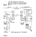
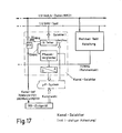
- the channel selector module - dash-dotted framed part - works strictly hierarchically through spatial and temporal sequential scanning in several, e.g. k levels. Accordingly, it requires k synchronous clock cycles, the generation of which will be discussed in more detail later. First of all, it can therefore be assumed that the clocks of 560 MHz, 280 MHz, 140 MHz and 70 MHz are available and available for a data stream on the signal-carrying line with a total bit rate of 1.12 Gbit / s.
- the serial data comes from the line, e.g. via an isolating amplifier, into the sampling stage circuit FF, which contains 4 stages in the selected example.
- the selected channel information is transmitted from the sampling stage circuit FF at a bit rate of e.g. 70 Mbit / s for color TV, 625 lines, or from 280 Mbit / s for HDTV to the BB terminal.
- the timing selector S delivers, corresponding to that via the BB terminal selected channel number, with the help of the synchronous clocks si also supplied to the individual stages of the scanning stage circuit FF, the associated signals.
- every second bit of the input bits which are halved in number from level to level and equidistant there, is faded out, and from all levels at least, from the last level only, the sequence that corresponds to the time slot of the selected channel is adopted.
- each flip-flop FF1, FF2, FF3, FF4 are supplied with the associated synchronous clocks clsl, cls2, cls3, cls4 and the relevant selection signals sl, s2, s3, s4 via a respective gate EXOR1, EXOR2, EXOR3, EXOR4.
- Running timers ⁇ 1, ⁇ 2, T 3, T 4 in the feed lines of the synchronous clocks enable an optimal setting of the phase positions for the input and control signals at the respective flip-flop FFi.
- the selection signals si are either “high” or “low”, in accordance with the selected channel position, while the synchronous clocks clsi periodically "high” and “low” with the associated frequency. This results in the output of a gate EXORi for the control input of a trigger circuit FFi as a clock signal cfi according to the table below:
- any of 16 possible outputs can be at the output of the sampling stage circuit FF in the selected example Time slots appear.
- the correspondingly higher-rate selected channel information can in general be readily taken after the second stage at 280 Mbit / s.
- a fast flip-flop of the Fairchild 11C series for example FllC06
- a module F100131 can be used for the following stages FF2, FF3, FF4.
- the gates EXOR2, EXOR3, EXOR4 can be constructed with the module F100107, the gate EXORl with a simple discrete circuit using ECL, E 2 CL , B CL technology or similar. This results in a 3 to 4 chip solution with a little additional wiring.
- the power consumption is correspondingly low and is around 1.5 W for such a four-stage 1.12 Gbit / s channel selector for 16 broadband channels.
- FIG. 10 shows such a variant, in which the last two stages are combined to form a scanning stage FF3.4. According to the previous explanations, the associated control need not be explained in more detail and can be seen solely from FIG. 10. Instead of tapping the sampling stage circuit FF for the selection of a 280 Mbit / s channel information after the second stage FF2, this information can also be obtained at the end output for 70 Mbit / s per se, if the gates EXOR3 and EXOR4 are controlled accordingly.
- the last two stages are combined in a flip-flop FF3.4, ie the third stage does not appear as a discrete stage.
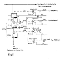
- the peculiarity of this embodiment relates to the second stage. Since the module used allows two flip-flops to be used for this purpose, these are operated as FF2a and FF2b at the limit of their maximum working speed with an optimally set sampling phase position in the division of labor, for the explanation of which a little more detail is given below.
- a single bit has a time length of about 0.9 ns.
- the first stage - FFl e.g. FllC06 - every second, whereby the rising edge of the clock pulse cfl for FFl is set fairly precisely to the middle of the bit duration.
- phase positions of the clock pulses cfl and cf2 depending on the combination of the selection signals sl and s2, there are two possibilities: either a clock pulse cf2 lies exactly between two clock pulses cfl or they have the phase difference O. That means for the Case that the clock pulse cf2 optimally on the time length of the signal to be sampled, ie on the middle, it is set that when sl and a corresponding offset of the clock pulse cfl by 0.9 ns, the clock pulse cf2 now exactly meets the boundary between two bits to be scanned, so here it gives the most unfavorable conditions.
- this is remedied by division of labor between the two flip-flops FF2a and FF2b, one of which always offers the optimal conditions when the other provides the most unfavorable conditions.
- These two flip-flops FF2a, FF2b are supplied with the signals to be processed, each shifted by 0.9 ns from one another, from the first stage.
- a delay element T is used in the signal feed to the one of the two flip-flops, in the example shown at FF2a.
- the same clock pulse cf2 is supplied to both flip-flops FF2a and FF2b.
- the scanning conditions are bad, for example with flip-flop FF2a, they are optimal with flip-flop FF2b and vice versa. Accordingly, after the set / clear inputs of the flip-flops FF2a and FF2b, the signals sl, sl are supplied from the control of the first stage FFl, that is to say only the flip-flop FF2a or FF2b which optimally perform the scanning under the given conditions can be unlocked, the other Toggle switch, FF2b or FF2a, is blocked at the same time.
- a F100107 module contains a total of 5 gates, of which only four are required to control the scanning stages.
- the fifth gate can now e.g. be used for the delay time of a signal, i.e. at least partially replace a delay line. In the embodiment shown in FIG. 11, this can expediently be implemented for the delay element r in the feed of the synchronous clock cls4 to the gate EXOR3.
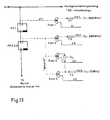
- stages 1 and 2 as well as 3 and 4 are combined in a flip-flop FF1.2 and FF3.4 for a 1:16 division. Compared to the previous explanations, no additional information is required.
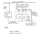
- FIG. 14 a modified variant of a channel selector for the derivation of the synchronous clock pulses can be provided in embodiments of the invention, as is shown, for example, in FIG. 14.
- This essentially consists of a channel selector circuit of the type already described.
- a detector for the synchronization pattern is connected to its output. This continuously recognizes and monitors the synchronization criteria in the channel and establishes or maintains the synchronism for the channel selector circuit.
- the control signals that take over the function of the selection signals are also derived from it.
- control information (sl, ..., sk) t ° was available at time t o and the synchronization pattern was not found on the signal-carrying line, the control information is changed so that (sl, ..., sk) to ⁇ ( sl , ..., sk) to + 1 .
- control clocks of this special synchronization channel selector are the so-called synchronous clocks. They can either be provided directly or, for example, via appropriate amplifiers, if necessary with an inverting device, clock drivers or the like, and in this way serve in particular for operating the channel selector circuits.
- FIG. 15 shows a complete circuit diagram for a Channel selector circuit which is connected to a signal-carrying line at 1.12 Gbit / s and whose principle of operation has been explained in connection with FIG. 11.
- Fig. 16 shows the layout and the layout plan for a realization in thick film technology, original size 5.08 x 2.54 cm (2 x 1 inch).
- the sampling stage can consist of a D flip-flop FF; such an element is for
- the current speed requirements are already on the market in an integrated form.
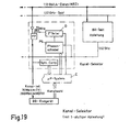
- FIG. 19 A further embodiment in accordance with the basic principle of channel selectors according to the invention is shown in FIG. 19:
- a sync-comparator sync comparator is available, with the aid of which a predetermined time position in the multiplex frame, ie the channel with the number O, is determined according to FIG. 3.
- This time slot generally serves as the starting point for setting a selected channel.
- a control C ensures the correct setting, both to find the starting position and to set a selected channel.
- phase shifter PS shows a basic circuit diagram for the phase shifter PS. It is necessary that with this phase shifter PS phase adjustments can be carried out without limitation, ie by more than 360 °. It should also only be used for a fixed frequency, here 1.12 GHz corresponding to the bit clock Clb, and has the task of shifting the time at which the subsequent frequency divider D outputs its output signal. However, since the frequency divider D can only reliably carry out time shifts by a full 1.12 GHz periods if this occurs in partial steps, the phase shifter PS is constructed from a plurality of delay elements Tp connected in series.
- Switches A, ..., H which lead in a star shape from the connection points between two delay elements to a central output of the phase shifter PS, are possible Chen shifts in such substeps. It is important that the closing times of switches A, ..., H to be operated one after the other always overlap for a short time.
- the RF signal fed in at the input is only transmitted to the central output if at least one of the switches A, ..., H is closed.
- a phase shift occurs when you switch from one switch to another. By the way, this is possible in both directions!
- the number of sub-steps for a full 1.12 GHz period must be greater than four in order to be able to safely adjust the subsequent frequency divider D. In preferred embodiments of the invention, however, eight substeps are provided. In this way, an additional fine adjustment of the sampling time of a 1.12 Gbit / s signal is possible, which is explained in more detail below. For such a fine adjustment, four sub-steps per 1.12 GHz period would not be enough, but more than eight sub-steps would no longer make sense.
- the phase shifter PS advantageously has phase adjustment steps that can be switched on cyclically one after the other.
- the phase adjustment or partial steps of a cycle correspond to the duration of a full 1.12 GHz period.
- a chain with e.g. Eight steps per cycle and a maximum required shift of 15 bits per 0.893 ns duration are too complex.
- the eight phase adjustment steps mentioned per 1.12 GHz period each correspond to a 45 ° phase shift.
- phase shifter PS So that the frequency divider D controlled by the phase shifter PS can be reliably adjusted by more than a 1.12 GHz period, the sub-steps of the phase shifter PS must be able to be carried out several times in a cyclical sequence. But this also means that the control signal for the phase shifter PS for 360 ° and 0 ° phase shift must be the same.
- the phase positions are changed in the following way: Assume switch A is closed. Then the supplied RF signal goes directly to the output of the phase shifter PS without delay - transit times within a switch and the relevant supply lines should be negligible here. To avoid signal interruptions, the next switch, here switch B, must be switched on before switch A is opened.
- the signal reaching the output via the first delay element ⁇ p and the switch B is - corresponding to 1/8 of a full 1.12 GHz period - delayed by 111.6 ps compared to the signal running via the switch A.
- an intermediate value ie a phase shift of approximately 22.5 ° or an average delay time of approximately 56 ps. So that the. Frequency divider D can be safely set to its new working time, should be provided for an adjustment of the phase position by 45 ° about 1 ⁇ s each (adjustment frequency thus about 1 MHz).
- phase shift of 315 0 resulted. There is no delay element between the switch H and the switch A. If switch A is now closed before switch H opens, the intermediate position of approx. 337.5 0 phase shift occurs at the output of the phase shifter PS. After opening switch H, the closed switch A results in a 360 ° phase shift.
- phase shifts can be achieved with which the rising output signal of the subsequent frequency divider D is also shifted in time.
- each other can be carried out by a maximum of eight "round trips" of the phase shifter PS in one or the other direction.
- Such adjustment requires a maximum of 64 ⁇ s with the above-mentioned adjustment frequency of 1 MHz per 45 °.
- the D flip-flop FF can be matched as precisely as possible in time or well to the signal of the 1.12 Gbit / s data stream to be sampled.
- the middle of the data bit is favorable for this. Signal delay tolerances and changes can then be compensated for.
- phase shifter PS Of the individual phase positions that can be set within a full 1.12 GHz period in the phase shifter PS, about half of the positions relate to the edge regions of a data bit, the other half to the roof area. In order to find an optimal scanning position, the phase shifter PS is adjusted from the current position to both sides until the scanning is no longer carried out safely there. These two positions are registered; the positions between these two positions, for example with at least one position as a safety distance, are optimal and can be automatically determined as a result of the fine adjustment and used as a starting point for subsequent channel selection adjustments.
- monitoring can also be carried out during operation.
- 21 shows the basic circuit diagram of a digital 1: 2 n frequency divider D as used in preferred embodiments of the invention. It is simple to set up, particularly low in power and divides the input frequency of 1.12 GHz into a lower-frequency clock signal with steep edges, ie it generates the multiplex clock Clm from the bit clock Clb.
- the circuit of such a frequency divider D requires only a NAND gate and a delay line ⁇ D. If, for example, only a 70 MHz clock signal Clm is to be generated, the delay line ⁇ D must be corresponding to get voted. If, for example for HDTV channels, multiplex clock signals Clm of 280 MHz or 140 MHz are required, there are either correspondingly shorter delay lines TD or switchable taps on the long one Provide delay line.
- the suppression of the 1.12 GHz signal in the NAND gate is only necessary for the case in which the H state is present at input E2. However, it would not harm in the other case, in which the input E2 is in the L state and the 1.12 GHz signal does not affect the state of the NAND gate.
- such suppression is expediently implemented with a ⁇ / 4 stub open on the output side. This acts on a signal of wavelength ⁇ like a short circuit.
- This frequency divider vibrates independently with its natural frequency f eigen 'when a signal in the H state is present at the input E 1 instead of the 1.12 GHz signal.
- the - Delivered by the phase shifter PS - 1.12 GHz input signal synchronizes the frequency divider D, that is, in the event of a phase or transit time change using the phase shifter PS, a period of the frequency divider D is lengthened or shortened, so that - as desired - the future periods accordingly later or start earlier.
- the third specific element of this channel selector is the sampling stage FF, for which FIG. 22 shows the basic circuit diagram. It is a circuit made up of individual components with an RS flip-flop, an AND gate, a delay element and possibly two pulse shape stages.
- the sampling stage FF is controlled by a positive pulse, approximately 0.9 ns wide, which is periodically in the multiplex clock Clm, e.g. 70 MHz or for HDTV 280 MHz, is supplied by the frequency divider D and reaches the reset input R of the flip-flop. This periodically ensures an L state at the Q output in the multiplex clock Clm. This state remains as long as there is no signal in the H state at set input S.
- a positive set pulse can only be generated by the AND gate if a 1.12 Gbit / s data bit is present in the H state at the time of the control pulse at the AND gate input. Such a set pulse ensures an L state at the Q output.
- the flip-flop could not assume a defined state. For this reason, the set pulse is compared to the reset pulse with ei nem delay element ⁇ s delayed in time. The pulse that is later to be applied is therefore decisive for the flip-flop state in each multiplex clock period.
- the iQ output changes to the L state and the Q output to the H state for the duration of a multiplex clock cycle.
- the Q output can therefore assume two states during a multiplex clock period, but the Q output can only have one. Therefore only the data of the Q -Processed output, in particular led through an inverting amplifier.
- the starting position must be determined from which the selected channel is then sought.
- the starting position is the time position of channel No. O - cf. Fig. 3 - which is, at least partially, occupied with the synchronization data pattern.
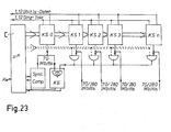
- one of the channel selectors KS here the channel selector KSO, is controlled by the microprocessor controller C via a control bus via the synchronization character comparator Sync.-COMP to the synchronization data pattern of the serial input data stream.
- the controller C causes the channel selector KSO to examine other time positions of the serial data stream by stepwise, overlapping phase shifts.
- the channel selector KSO is thus optimally set as a channel selector for the synchronization channel. It provides the starting point for the setting of a channel selected by the channel selection information Kw.
- Such a setting runs, for example, as follows.
- the channel selector KS 1 was assigned to the subscriber's broadband terminal which was put into operation. This is now set by the control C to the synchronization channel via the control bus, i.e. brought into the starting position already found by the channel selector KSO.
- a channel monitoring circuit K-COMP is used, which is made up of an EX-OR gate and a register. Control C switches the outputs of channel selectors KSO and KS 1 to the inputs of the EX-OR gate.
- possible data bit deviations are registered as errors and any necessary different scanning positions are caused in the fine adjustment of the channel selector KS 1 compared to that of the channel selector KSO.
- the controller C causes the phase shifter PS of the channel selector KS 1, n to pass through multiples of full adjustment step cycles (n corresponding to the distance between the synchronization channel and the selected channel) via the control bus.
- the adjustment is carried out in one or the other direction, of course on the shorter path.
- channel selectors KS in this modular he expandable channel selector system is practically unlimited. Their minimum number depends on the number of connected BB terminals or on the number of selectable channels, in which case several broadband terminals for which the same channel has been selected must be connected to the same channel selector.
- the microprocessor control C is advantageously also designed to carry out monitoring and correction tasks. For example, those channel selectors that are not currently in operation can be set to the starting position as a precaution in order to shorten the setting time when a channel is actually selected.
- a setting of a selected channel with a channel selector KS that is already active does not necessarily have to start from the synchronization channel.
- the previously selected channel can also serve as a starting point.
- the monitoring system allows changes in signal propagation time to occur in the high-frequency circuits, e.g. caused by temperature fluctuations or aging, early detection of small deviations and automatic correction.
- modules M V which are assigned to a broadband terminal and contain the D flip-flop FF, the frequency divider D and the phase shifter PS.
- a complete channel selector circuit can thus be formed for a single terminal device to be operated, i.e. a sync-comparator Sync.-COMP and a microprocessor control C, possibly also a channel monitoring circuit K-COMP, have to be added.
- a module M VI with all these elements mentioned, which can be expanded as desired by adding modules M V and is thus assigned to several channel selector circuits located at a subscriber station.
- FIG. 24 shows the overall circuit diagram for the specific elements of this channel selector circuit, namely for the phase shifter PS (part 1 of FIG. 24), the fre frequency divider D (part 2) and the sampling stage FF (part 3 of FIG. 24).
- a circuit not shown, known per se with a phase locked loop (see, for example, DE-A 28 54 039) or the like is used.
- the circuit shown in FIG. 24 was realized as a thick film circuit, original size (5 0 , 8 x 76.2) mm 2 (2 "x 3") and has a power consumption of almost 700 mW. When optimizing the circuit, it is to be expected that the power requirement is approximately 500 mW.
- the MV / M VI modules are also suitable for implementation as integrated circuits (IC).
- Part 1 phase shifter, PS
Landscapes
- Engineering & Computer Science (AREA)
- Multimedia (AREA)
- Signal Processing (AREA)
- Computer Networks & Wireless Communication (AREA)
- Color Television Systems (AREA)
- Time-Division Multiplex Systems (AREA)
Applications Claiming Priority (6)
| Application Number | Priority Date | Filing Date | Title |
|---|---|---|---|
| DE19833310412 DE3310412A1 (de) | 1983-03-18 | 1983-03-18 | Kanalwaehlerschaltung fuer digitale, bitweise verschachtelte breitbandkanaele |
| DE3310412 | 1983-03-18 | ||
| DE3310411 | 1983-03-18 | ||
| DE19833310411 DE3310411A1 (de) | 1983-03-18 | 1983-03-18 | Kanalwaehlerschaltung fuer digitale, bitweise verschachtelte breitbandkanaele |
| DE3318484 | 1983-05-19 | ||
| DE19833318484 DE3318484A1 (de) | 1983-05-19 | 1983-05-19 | Kanalwaehlerschaltung fuer digitale, bitweise verschachtelte breitbandkanaele |
Publications (2)
| Publication Number | Publication Date |
|---|---|
| EP0120806A2 true EP0120806A2 (fr) | 1984-10-03 |
| EP0120806A3 EP0120806A3 (fr) | 1986-07-30 |
Family
ID=27190863
Family Applications (1)
| Application Number | Title | Priority Date | Filing Date |
|---|---|---|---|
| EP84730024A Withdrawn EP0120806A3 (fr) | 1983-03-18 | 1984-03-16 | Circuit sélecteur de canal pour des canaux numériques à large bande à intercalage de bits |
Country Status (1)
| Country | Link |
|---|---|
| EP (1) | EP0120806A3 (fr) |
Cited By (3)
| Publication number | Priority date | Publication date | Assignee | Title |
|---|---|---|---|---|
| EP0205863A1 (fr) * | 1985-06-05 | 1986-12-30 | ANT Nachrichtentechnik GmbH | Système de distribution de communications à large bande |
| FR2584256A1 (fr) * | 1985-06-28 | 1987-01-02 | Thomson Csf | Procede de multiplexage et de demultiplexage temporels de signaux video et de signaux a bande etroite, et dispositifs pour la mise en oeuvre de ce procede |
| EP0212261A1 (fr) * | 1985-08-20 | 1987-03-04 | ANT Nachrichtentechnik GmbH | Système de distribution et de communication à large bande |
Family Cites Families (3)
| Publication number | Priority date | Publication date | Assignee | Title |
|---|---|---|---|---|
| FR2349243A1 (fr) * | 1976-04-23 | 1977-11-18 | Telecommunications Sa | Systeme de transmission numerique a division du temps |
| US4393516A (en) * | 1979-03-09 | 1983-07-12 | Electric Power Research Institute, Inc. | Data transmission system and method |
| DE2922418C2 (de) * | 1979-06-01 | 1981-12-03 | Licentia Patent-Verwaltungs-Gmbh, 6000 Frankfurt | Dienstintegriertes Nachrichtenübertragungs- und Vermittlungssystem für Ton, Bild und Daten |
-
1984
- 1984-03-16 EP EP84730024A patent/EP0120806A3/fr not_active Withdrawn
Cited By (3)
| Publication number | Priority date | Publication date | Assignee | Title |
|---|---|---|---|---|
| EP0205863A1 (fr) * | 1985-06-05 | 1986-12-30 | ANT Nachrichtentechnik GmbH | Système de distribution de communications à large bande |
| FR2584256A1 (fr) * | 1985-06-28 | 1987-01-02 | Thomson Csf | Procede de multiplexage et de demultiplexage temporels de signaux video et de signaux a bande etroite, et dispositifs pour la mise en oeuvre de ce procede |
| EP0212261A1 (fr) * | 1985-08-20 | 1987-03-04 | ANT Nachrichtentechnik GmbH | Système de distribution et de communication à large bande |
Also Published As
| Publication number | Publication date |
|---|---|
| EP0120806A3 (fr) | 1986-07-30 |
Similar Documents
| Publication | Publication Date | Title |
|---|---|---|
| DE2728686C2 (fr) | ||
| DE69231871T2 (de) | Verfahren zur parallelen Übertragung | |
| DE69432587T2 (de) | Verzögerungsleitungsseparator für datenbus | |
| DE2758797C2 (de) | Umsetzer zum Umsetzen von Serien-Kanal-Daten einer Vielzahl von primären digitalen Multiplexstrecken in Parallel-Kanal-Daten | |
| DE2740347A1 (de) | Vorrichtung zum einfuegen und ausblenden von zusatzinformation in einen bzw. aus einem digitalen informationsstrom | |
| DE2315247B2 (de) | Fernmeldesystem mit einzelnen durch einen gemeinsamen Kanal verbundenen Sender-Empfänger-Stationen | |
| DE68922930T2 (de) | Impulseinblendungsanordnung. | |
| DE2924922C2 (fr) | ||
| DE69031557T2 (de) | Zellensignalverarbeitungsschaltung und optische Vermittlungseinrichtung unter Anwendung dieser Schaltung | |
| DE3927681A1 (de) | Verfahren zur zwischenverstaerkung von digitalen signalen sowie zwischenverstaerker fuer digitale signale | |
| EP0007524A1 (fr) | Procédé et circuit pour la transmission de données | |
| DE2149911C3 (de) | Schaltungsanordnung zur gegenseitigen Synchronisierung der in den Vermittlungsstellen eines PCM-Zeitmultiplexfernmeldenetzes vorgesehenen Amtstaktoszillatoren | |
| DE3785906T2 (de) | Kanalersatzschaltungssystem für ein Funkübertragungssystem von digitalen Daten. | |
| DE60107899T2 (de) | Parallele Datenschnittstelle | |
| EP0363513A1 (fr) | Procedé et dispositif de réception d'un signal numérique binaire | |
| DE69225320T2 (de) | Adapter zum Anschluss an ein "clear channel"-Übertragungsnetz | |
| EP0120806A2 (fr) | Circuit sélecteur de canal pour des canaux numériques à large bande à intercalage de bits | |
| EP0103163A2 (fr) | Dispositif pour le démultiplexage synchrone d'un signal multiplex à division de temps | |
| DE69423646T2 (de) | Sendersynchronisierte datenübertragungsanordnung | |
| DE3230027A1 (de) | Synchronisieranordnung | |
| DE102005008503B3 (de) | Verfahren und Netzwerk zur Daten- und Signalübertragung | |
| DE2242639C3 (de) | Zeitmultiplex-Telegrafie-System für zeichenweise Verschachtelung | |
| DE3129731A1 (de) | Digitales breitband-kommunikationssystem | |
| DE1279768B (de) | Verfahren und Schaltungsanordnung zur Vervielfachung der Bandbreite von Nachrichtenkanaelen in Zeitmultiplex-Vermittlungsanlagen | |
| EP0418641B1 (fr) | Dispositif de synchronisation pour un signal numérique |
Legal Events
| Date | Code | Title | Description |
|---|---|---|---|
| PUAI | Public reference made under article 153(3) epc to a published international application that has entered the european phase |
Free format text: ORIGINAL CODE: 0009012 |
|
| AK | Designated contracting states |
Designated state(s): AT BE CH DE FR GB IT LI LU NL SE |
|
| PUAL | Search report despatched |
Free format text: ORIGINAL CODE: 0009013 |
|
| RHK1 | Main classification (correction) |
Ipc: H04J 3/04 |
|
| AK | Designated contracting states |
Kind code of ref document: A3 Designated state(s): AT BE CH DE FR GB IT LI LU NL SE |
|
| STAA | Information on the status of an ep patent application or granted ep patent |
Free format text: STATUS: THE APPLICATION IS DEEMED TO BE WITHDRAWN |
|
| 18D | Application deemed to be withdrawn |
Effective date: 19870130 |
|
| RIN1 | Information on inventor provided before grant (corrected) |
Inventor name: LUKANEK, FRANK Inventor name: HEYDT, GUENTER Inventor name: TEICH, GEORG |