EP0120992A2 - AND-gate driver circuit - Google Patents
AND-gate driver circuit Download PDFInfo
- Publication number
- EP0120992A2 EP0120992A2 EP83111939A EP83111939A EP0120992A2 EP 0120992 A2 EP0120992 A2 EP 0120992A2 EP 83111939 A EP83111939 A EP 83111939A EP 83111939 A EP83111939 A EP 83111939A EP 0120992 A2 EP0120992 A2 EP 0120992A2
- Authority
- EP
- European Patent Office
- Prior art keywords
- circuit
- gate
- fet device
- output node
- output
- Prior art date
- Legal status (The legal status is an assumption and is not a legal conclusion. Google has not performed a legal analysis and makes no representation as to the accuracy of the status listed.)
- Granted
Links
Images

Classifications
-
- H—ELECTRICITY
- H03—ELECTRONIC CIRCUITRY
- H03K—PULSE TECHNIQUE
- H03K19/00—Logic circuits, i.e. having at least two inputs acting on one output; Inverting circuits
- H03K19/02—Logic circuits, i.e. having at least two inputs acting on one output; Inverting circuits using specified components
- H03K19/08—Logic circuits, i.e. having at least two inputs acting on one output; Inverting circuits using specified components using semiconductor devices
- H03K19/094—Logic circuits, i.e. having at least two inputs acting on one output; Inverting circuits using specified components using semiconductor devices using field-effect transistors
- H03K19/0944—Logic circuits, i.e. having at least two inputs acting on one output; Inverting circuits using specified components using semiconductor devices using field-effect transistors using MOSFET or insulated gate field-effect transistors, i.e. IGFET
- H03K19/09441—Logic circuits, i.e. having at least two inputs acting on one output; Inverting circuits using specified components using semiconductor devices using field-effect transistors using MOSFET or insulated gate field-effect transistors, i.e. IGFET of the same canal type
- H03K19/09443—Logic circuits, i.e. having at least two inputs acting on one output; Inverting circuits using specified components using semiconductor devices using field-effect transistors using MOSFET or insulated gate field-effect transistors, i.e. IGFET of the same canal type using a combination of enhancement and depletion transistors
- H03K19/09445—Logic circuits, i.e. having at least two inputs acting on one output; Inverting circuits using specified components using semiconductor devices using field-effect transistors using MOSFET or insulated gate field-effect transistors, i.e. IGFET of the same canal type using a combination of enhancement and depletion transistors with active depletion transistors
-
- H—ELECTRICITY
- H03—ELECTRONIC CIRCUITRY
- H03K—PULSE TECHNIQUE
- H03K19/00—Logic circuits, i.e. having at least two inputs acting on one output; Inverting circuits
- H03K19/01—Modifications for accelerating switching
- H03K19/017—Modifications for accelerating switching in field-effect transistor circuits
- H03K19/01707—Modifications for accelerating switching in field-effect transistor circuits in asynchronous circuits
- H03K19/01714—Modifications for accelerating switching in field-effect transistor circuits in asynchronous circuits by bootstrapping, i.e. by positive feed-back
Definitions
- None of this prior art shows the use of a "natural" threshold device which is serially connected between the gate of the output depletion mode FET device and the input node to the circuit providing current flow from the input node to the gate of the FET device as the input waveform begins to rise, and yet providing sufficient resistance in the gate circuit of the output FET so as to prevent backward flow of current from the gate as the potential of the output node rises.
- One of the main advantages offered by the invention is the effective increase in the conductivity of the load device of the circuit whereby shorter rise times of the output waveforms are obtained. It also provides for less power dissipation and reduced active circuit area requirements.
- a "natural" threshold device is serially connected between the gate of an output FET load device and the input node to the circuit so as to provide current flow from the input node to the gate of the FET load device as the input waveform begins to rise, and yet to provide sufficient resistance in the gate circuit of the FET load device so as to prevent backward flow of current from the gate thereof as the potential of the output node rises. This increases the conductivity of the output load device, thereby providing a faster rise time for the output waveform.
- the gate of device 6' which is an output depletion mode FET device, is connected through a self-biased depletion mode load device 8' to the drain potential VDD in what is effectively a short connection to VDD.
- the zero threshold voltage "natural" FET device 4 in the AND driver invention of Figures 2 and 3 presents a certain amount of resistive impedance which is serially connected between the gate of the output FET load device 6 and the input node to the circuit at FET device 3.
- both the source and the gate of the natural device 4 are at the same potential and the device 4 will be in its on state so that current will flow from the input node to the FET device 3 through the natural device 4 to the node P13 at the gate of the FET device 6.
- the gate-to-source capacitance of the FET device 6 couples the rise in the potential at the output node to the node P13 which is the gate of the FET device 6. Since there is some resistance in the series connected natural FET device 4, although a charge will start to slowly flow from the node P13 through the FET device 4, it will not flow out fast enough to avoid the bootstrapping effect wherein the potential at the gate of the FET device 6 rises above the value of VDD due to the capacitive coupling of the gate of the FET device 6 to its source.
- the AND gate driver circuit of Figures 2 and 3 comprises a NAND block 1, 2 and 3 having a first and second input terminals and an output node, for providing a NAND logic function voltage at the output thereof in response to the voltages applied to the input terminals.
- An output circuit including the enhancement mode FET device 7 is connected between the circuit output node and ground potential, having its gate connected to the output node of the NAND block.
- the low threshold voltage FET device 6 is connected between the circuit output node and the drain potential, having its gate connected through an impedance 5 to the ground potential.
- the substantially zero threshold voltage FET device 4 has its source/drain path connected between the gate of the low threshold voltage FET device 6 and a first one of the circuit inputs, and also has its gate connected to a second one of the circuit inputs.
- the zero threshold device 4 conducts current between the first one of the circuit inputs and the gate of the low threshold FET device when the potential of the first input begins to rise, and the zero threshold device 4 impedes current flow between the gate of the low threshold FET device and the first one of the circuit inputs when the voltage at the circuit output node rises. Therefore the rise time of the voltage at the circuit output node is reduced.
- the resultant AND driver circuit will drive a capacitive load at the output node with a faster rise time than is available with conventional bootstrap circuits. Analysis shows the circuit to be approximately 10 percent faster with 24 percent less power dissipation. Physical layouts of the circuit indicate that it will occupy 5 percent less active area than the conventional driver circuits, such as is shown in Figure 1.
- the second embodiment of the invention is shown in Figure 3.
- the FET device 5 is a self-biased depletion mode load device which serves as a diode-type impedance between the bootstrap node and the ground potential and serves to bleed charge from node P13.
- the FET device 5 is an enhancement mode FET device whose gate is connected to the output node of the first stage, so as to serve as an active impedance between the bootstrap node and ground potential.
- device 5 serves to bleed charge from node P13 during intervals when the output P10 is going low.
- the active impedance embodiment of Figure 2 is faster in that it provides a quicker on-state rise time because more positive charge remains at the gate of device 6, since device 5 is turned off when the output P10 is going high.
Landscapes
- Engineering & Computer Science (AREA)
- Physics & Mathematics (AREA)
- Computer Hardware Design (AREA)
- Computing Systems (AREA)
- General Engineering & Computer Science (AREA)
- Mathematical Physics (AREA)
- Power Engineering (AREA)
- Logic Circuits (AREA)
- Manipulation Of Pulses (AREA)
- Electronic Switches (AREA)
Abstract
Description
- The invention disclosed broadly relates to semiconductor circuits and more particularly relates to an AND gate driver circuit comprising:
- a NAND block having a first and second input terminals and an output node, for providing a NAND logic function voltage at the output node in response to the voltages applied to the input terminals;
- an output circuit including an enhancement mode FET device connected between a circuit output node and ground potential, having its gate connected to the output node of said NAND block; and
- a low threshold voltage FET device connected between the circuit output node and a drain potential, having its gate connected through an impedance means to said ground potential.
- In conventional push/pull AND drivers (such as that shown in Figure 1) the gate of the output depletion mode FET device is connected through a self-biased depletion mode load device to the drain potential in what is effectively a shorted connection to drain potential. Thus, as the output node for the circuit rises, there is no chance for any bootstrapping effect to take place through the gate-to-source capacitance, since the gate potential for the output device cannot rise above the drain potential. This limits the rise time for output waveforms from the driver circuit.
- Representative of the state of the art are articles "Bootstrapped Decoder Circuit for low Supply Voltage Applications" (published in IBM Technical Disclosure Bulletin, Vol. 24, No. 11B, April 1982, page 5910) and "Bootstrap Positive AND-Circuit" (published in IBM Technical Disclosure Bulletin, Vol. 13, No. 7, December 1970, page 1877). Other prior art includes US Patents 3.541.353, 4.048.518, 3.832.574, and 3.601.630.
- None of this prior art shows the use of a "natural" threshold device which is serially connected between the gate of the output depletion mode FET device and the input node to the circuit providing current flow from the input node to the gate of the FET device as the input waveform begins to rise, and yet providing sufficient resistance in the gate circuit of the output FET so as to prevent backward flow of current from the gate as the potential of the output node rises.
- It is therefore an object of the invention to achieve a faster time for an output waveform from an FET driver - circuit.
- These and other objects, features and advantages of the invention are accomplished by the AND gate driver circuit disclosed and claimed herein.
- One of the main advantages offered by the invention is the effective increase in the conductivity of the load device of the circuit whereby shorter rise times of the output waveforms are obtained. It also provides for less power dissipation and reduced active circuit area requirements.
- Two ways of carrying out the invention are described in detail below with reference to drawings which illustrate specific embodiments, and in which
- Figure 1 illustrates a prior art FET driver circuit.
- Figure 2 illustrates the improved high performance AND gate driver circuit in accordance with the invention, and includes an
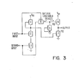
active impedance device 5. - Figure 3 illustrates a second embodiment of the invention, and includes a diode-
type impedance device 5. - A "natural" threshold device is serially connected between the gate of an output FET load device and the input node to the circuit so as to provide current flow from the input node to the gate of the FET load device as the input waveform begins to rise, and yet to provide sufficient resistance in the gate circuit of the FET load device so as to prevent backward flow of current from the gate thereof as the potential of the output node rises. This increases the conductivity of the output load device, thereby providing a faster rise time for the output waveform.
- In the conventional push/pull AND driver of Figure 1, consisting of the FET devices 1' to 8', the gate of device 6' which is an output depletion mode FET device, is connected through a self-biased depletion mode load device 8' to the drain potential VDD in what is effectively a short connection to VDD. Thus, as the output node for the circuit rises, there is no chance for a bootstrapping effect to take place through the gate-to-source capacitance, since the gate potential for the output device 6' cannot rise above the VDD potential. This limits the rise time for output waveforms from the driver circuit.
- In contrast, the zero threshold voltage "natural"
FET device 4 in the AND driver invention of Figures 2 and 3, presents a certain amount of resistive impedance which is serially connected between the gate of the outputFET load device 6 and the input node to the circuit atFET device 3. When the input node to theFET device 3 undergoes a positive transition and the input node to theFET device 2 undergoes a positive transition, both the source and the gate of thenatural device 4 are at the same potential and thedevice 4 will be in its on state so that current will flow from the input node to theFET device 3 through thenatural device 4 to the node P13 at the gate of theFET device 6. - Thereafter, as the output node P10 of the circuit rises, the gate-to-source capacitance of the
FET device 6 couples the rise in the potential at the output node to the node P13 which is the gate of theFET device 6. Since there is some resistance in the series connectednatural FET device 4, although a charge will start to slowly flow from the node P13 through theFET device 4, it will not flow out fast enough to avoid the bootstrapping effect wherein the potential at the gate of theFET device 6 rises above the value of VDD due to the capacitive coupling of the gate of theFET device 6 to its source. - As an example, when VDD equals 4.5 volts and the input voltages at the
FET devices - This forces the
load device 6 into a strong on-state, thereby providing a greater quantity of current to the output node P10. As a result, the AND driver invention of Figures 2 and 3 will drive a capacitive load at the output node of the circuit with a faster rise time than is available with the more conventional push/pull circuit of Figure 1. - The AND gate driver circuit of Figures 2 and 3 comprises a
NAND block mode FET device 7 is connected between the circuit output node and ground potential, having its gate connected to the output node of the NAND block. The low thresholdvoltage FET device 6 is connected between the circuit output node and the drain potential, having its gate connected through animpedance 5 to the ground potential. The substantially zero thresholdvoltage FET device 4 has its source/drain path connected between the gate of the low thresholdvoltage FET device 6 and a first one of the circuit inputs, and also has its gate connected to a second one of the circuit inputs. The zerothreshold device 4 conducts current between the first one of the circuit inputs and the gate of the low threshold FET device when the potential of the first input begins to rise, and the zerothreshold device 4 impedes current flow between the gate of the low threshold FET device and the first one of the circuit inputs when the voltage at the circuit output node rises. Therefore the rise time of the voltage at the circuit output node is reduced. - The resultant AND driver circuit will drive a capacitive load at the output node with a faster rise time than is available with conventional bootstrap circuits. Analysis shows the circuit to be approximately 10 percent faster with 24 percent less power dissipation. Physical layouts of the circuit indicate that it will occupy 5 percent less active area than the conventional driver circuits, such as is shown in Figure 1.
- The second embodiment of the invention is shown in Figure 3. The difference between the embodiments in Figures 2 and 3 lies in the
FET device 5. In the embodiment shown in Figure 3, theFET device 5 is a self-biased depletion mode load device which serves as a diode-type impedance between the bootstrap node and the ground potential and serves to bleed charge from node P13. In the embodiment shown in Figure 2, theFET device 5 is an enhancement mode FET device whose gate is connected to the output node of the first stage, so as to serve as an active impedance between the bootstrap node and ground potential. In both embodiments,device 5 serves to bleed charge from node P13 during intervals when the output P10 is going low. The active impedance embodiment of Figure 2 is faster in that it provides a quicker on-state rise time because more positive charge remains at the gate ofdevice 6, sincedevice 5 is turned off when the output P10 is going high. - Although specific embodiments of the invention have been disclosed, it will be understood by those of skill in the art that the foregoing and other changes in form and details may be made therein without departing from the spirit and the scope of the invention.
Claims (3)
Applications Claiming Priority (2)
| Application Number | Priority Date | Filing Date | Title |
|---|---|---|---|
| US06/481,033 US4525640A (en) | 1983-03-31 | 1983-03-31 | High performance and gate having an "natural" or zero threshold transistor for providing a faster rise time for the output |
| US481033 | 1983-03-31 |
Publications (3)
| Publication Number | Publication Date |
|---|---|
| EP0120992A2 true EP0120992A2 (en) | 1984-10-10 |
| EP0120992A3 EP0120992A3 (en) | 1985-07-31 |
| EP0120992B1 EP0120992B1 (en) | 1987-11-25 |
Family
ID=23910318
Family Applications (1)
| Application Number | Title | Priority Date | Filing Date |
|---|---|---|---|
| EP83111939A Expired EP0120992B1 (en) | 1983-03-31 | 1983-11-29 | And-gate driver circuit |
Country Status (4)
| Country | Link |
|---|---|
| US (1) | US4525640A (en) |
| EP (1) | EP0120992B1 (en) |
| JP (1) | JPS59185429A (en) |
| DE (1) | DE3374747D1 (en) |
Families Citing this family (4)
| Publication number | Priority date | Publication date | Assignee | Title |
|---|---|---|---|---|
| US4616147A (en) * | 1984-11-15 | 1986-10-07 | Motorola, Inc. | Programmable edge defined output buffer |
| US4629908A (en) * | 1985-02-19 | 1986-12-16 | Standard Microsystems Corp. | MOS monostable multivibrator |
| JPH07114359B2 (en) * | 1989-07-28 | 1995-12-06 | 株式会社東芝 | Semiconductor integrated circuit |
| EP4064349A1 (en) | 2013-11-15 | 2022-09-28 | Texas Instruments Incorporated | Method and circuitry for controlling a depletion-mode transistor |
Family Cites Families (10)
| Publication number | Priority date | Publication date | Assignee | Title |
|---|---|---|---|---|
| US3832574A (en) * | 1972-12-29 | 1974-08-27 | Ibm | Fast insulated gate field effect transistor circuit using multiple threshold technology |
| JPS5178665A (en) * | 1974-12-24 | 1976-07-08 | Ibm | |
| US3995172A (en) * | 1975-06-05 | 1976-11-30 | International Business Machines Corporation | Enhancement-and depletion-type field effect transistors connected in parallel |
| JPS522266A (en) * | 1975-06-24 | 1977-01-08 | Hitachi Ltd | Mos push-pull circuit |
| JPS5368555A (en) * | 1976-12-01 | 1978-06-19 | Hitachi Ltd | Pulse circuit |
| JPS53125753A (en) * | 1977-04-08 | 1978-11-02 | Nec Corp | Driving circuit |
| JPS6035756B2 (en) * | 1977-12-27 | 1985-08-16 | 日本電気株式会社 | logic circuit |
| DE2816980C3 (en) * | 1978-04-19 | 1980-10-09 | Ibm Deutschland Gmbh, 7000 Stuttgart | FET driver circuit with short switching times |
| US4289973A (en) * | 1979-08-13 | 1981-09-15 | Mostek Corporation | AND-gate clock |
| US4381460A (en) * | 1980-05-27 | 1983-04-26 | National Semiconductor Corporation | Bootstrap driver circuit |
-
1983
- 1983-03-31 US US06/481,033 patent/US4525640A/en not_active Expired - Fee Related
- 1983-11-29 DE DE8383111939T patent/DE3374747D1/en not_active Expired
- 1983-11-29 EP EP83111939A patent/EP0120992B1/en not_active Expired
- 1983-11-29 JP JP58223388A patent/JPS59185429A/en active Granted
Also Published As
| Publication number | Publication date |
|---|---|
| EP0120992B1 (en) | 1987-11-25 |
| DE3374747D1 (en) | 1988-01-07 |
| JPS59185429A (en) | 1984-10-22 |
| JPH0363853B2 (en) | 1991-10-02 |
| US4525640A (en) | 1985-06-25 |
| EP0120992A3 (en) | 1985-07-31 |
Similar Documents
| Publication | Publication Date | Title |
|---|---|---|
| JP2996301B2 (en) | Load and time adaptive current supply drive circuit | |
| US4300065A (en) | Power on reset circuit | |
| US3906254A (en) | Complementary FET pulse level converter | |
| US4176289A (en) | Driving circuit for integrated circuit semiconductor memory | |
| JPH08251014A (en) | Device having dynamic logic circuit, method of manufacturing the device, and signal processing method | |
| EP0055601A2 (en) | Buffer circuit | |
| US4725746A (en) | MOSFET buffer circuit with an improved bootstrapping circuit | |
| JPH0368473B2 (en) | ||
| US4112296A (en) | Data latch | |
| EP0047366A1 (en) | Transistor driver circuit | |
| US4894559A (en) | Buffer circuit operable with reduced power consumption | |
| EP0032017A1 (en) | Bootstrap circuit | |
| US4347448A (en) | Buffer circuit for semiconductor memory | |
| US4317051A (en) | Clock generator (buffer) circuit | |
| US5210449A (en) | Edge triggered tri-state output buffer | |
| US4239991A (en) | Clock voltage generator for semiconductor memory | |
| US4296340A (en) | Initializing circuit for MOS integrated circuits | |
| US3986044A (en) | Clocked IGFET voltage level sustaining circuit | |
| US4352996A (en) | IGFET Clock generator circuit employing MOS boatstrap capacitive drive | |
| EP0063357B1 (en) | Drive circuit | |
| JPH0210517B2 (en) | ||
| JPH0716157B2 (en) | MOS high current output buffer | |
| EP0120992B1 (en) | And-gate driver circuit | |
| US5818264A (en) | Dynamic circuit having improved noise immunity and method therefor | |
| EP0068892A2 (en) | Inverter circuit |
Legal Events
| Date | Code | Title | Description |
|---|---|---|---|
| PUAI | Public reference made under article 153(3) epc to a published international application that has entered the european phase |
Free format text: ORIGINAL CODE: 0009012 |
|
| AK | Designated contracting states |
Kind code of ref document: A2 Designated state(s): DE FR GB |
|
| 17P | Request for examination filed |
Effective date: 19841123 |
|
| PUAL | Search report despatched |
Free format text: ORIGINAL CODE: 0009013 |
|
| AK | Designated contracting states |
Kind code of ref document: A3 Designated state(s): DE FR GB |
|
| 17Q | First examination report despatched |
Effective date: 19860919 |
|
| GRAA | (expected) grant |
Free format text: ORIGINAL CODE: 0009210 |
|
| AK | Designated contracting states |
Kind code of ref document: B1 Designated state(s): DE FR GB |
|
| REF | Corresponds to: |
Ref document number: 3374747 Country of ref document: DE Date of ref document: 19880107 |
|
| ET | Fr: translation filed | ||
| PLBE | No opposition filed within time limit |
Free format text: ORIGINAL CODE: 0009261 |
|
| STAA | Information on the status of an ep patent application or granted ep patent |
Free format text: STATUS: NO OPPOSITION FILED WITHIN TIME LIMIT |
|
| 26N | No opposition filed | ||
| REG | Reference to a national code |
Ref country code: FR Ref legal event code: ST |
|
| REG | Reference to a national code |
Ref country code: FR Ref legal event code: RC |
|
| REG | Reference to a national code |
Ref country code: FR Ref legal event code: DA |
|
| PGFP | Annual fee paid to national office [announced via postgrant information from national office to epo] |
Ref country code: GB Payment date: 19911008 Year of fee payment: 9 |
|
| PGFP | Annual fee paid to national office [announced via postgrant information from national office to epo] |
Ref country code: FR Payment date: 19911028 Year of fee payment: 9 |
|
| PGFP | Annual fee paid to national office [announced via postgrant information from national office to epo] |
Ref country code: DE Payment date: 19911118 Year of fee payment: 9 |
|
| PG25 | Lapsed in a contracting state [announced via postgrant information from national office to epo] |
Ref country code: GB Effective date: 19921129 |
|
| GBPC | Gb: european patent ceased through non-payment of renewal fee |
Effective date: 19921129 |
|
| PG25 | Lapsed in a contracting state [announced via postgrant information from national office to epo] |
Ref country code: FR Effective date: 19930730 |
|
| PG25 | Lapsed in a contracting state [announced via postgrant information from national office to epo] |
Ref country code: DE Effective date: 19930803 |
|
| REG | Reference to a national code |
Ref country code: FR Ref legal event code: ST |